

Page 1

KS7306 DIGITAL CAMERA PROCESSOR
ORDERING INFORMATION
GENERAL DESCRIPTION
100-QFP-1414
KS7306 is a CCD digital signal processor.
The electronic video signal that passed the color
filter array(CFA) pattern of CCD is put to the process
of dual correlation sampling and then converted to
digital video signal by A/D converter.
Taking the digital video signal so processed as an
input, KS7306 performs luminance and chroma
signal process and finally outputs signals encoded to
NTSC/PAL broadcast standards, and generates
detection signals for AE/AF/AWB.
Device Package
KS7306 100-QFP-1414
FEATURES
• Offers 10 bit input digital signal processing.
• Carries built-in 2H line memory.(10bit 1024)
• Performs Y signal processing.
• Performs C signal processing.
• Carries an encorder capable to NTSC/PAL dual form application.
• Carries built-in Y/C 2-channal DA converter.
• Carries built-in AE/AF/AWB detection system.
• Provides micom parallel interface.
• Micom capable to control variable parameters.
• Offers digital effects interfacing
• Suites Hi8/Normal CCD application.
• Suites 470K,520K,570K and 620K CCD controlled EIS system application.
• Supports 16:9 aspect wide TV (full mode) application.
APPLICATIONS
CCD camera ( camcorder, CCTV, digital still camera, etc.).
Operating Temperature
0 ~ 70 °C
VID-97-D004
February 1997
1
Page 2

KS7306 DIGITAL CAMERA PROCESSOR
VDDPO
VSSPO
PIN CONFIGURATION
UVIO3
UVIO2
UVIO1
UVIO0
VDDI
UVO3
UVO2
UVO1
UVO0
VSSI
CD9
CD8
CD7
CD6
VDDPO
CD5
CD4
CD3
CD2
VSSPO
CD1
CD0
FSC4
CBLK
CSYNC
YI2
YI1
YI3
YO3
YO1
YO2
YO0
75 74 73 72 71 70 69 68 67 66 65 64 63 62 61 60 59 58 57 56 55 54 53 52 51
76
77
78
79
80
81
82
83
84
85
86
87
88
89
90
91
92
93
94
95
96
97
98
99
100
C-Processor
VSSPO
YO4
YO5
NTSC/PAL Encoder
Line Memory
Pre-Processor
Timing Interface
YO6
YO7
YI0
VDDPO
Y-Processor
TEST
YI4
VSSI
YI5
YI6
YI7
TST2
Interface
Optical
Detector
MICOM
VDDI
DZCSYNCI
D/A
D/A
DZBFII
DZCBLKI
TST1
50
DZCBLKO
49
DZBFO
48
DZCSYNCO
47
UVCK
46
XCK
45
TST4
44
INDIR
43
VSSA
42
VDDA
41
AC
40
VREF
39
IREF
38
BCAP
37
AY
36
VDDA
VSSA
35
34
BFO
33
FSC
32
CSYNCO
31
AFZONE
30
TST3
29
VSYNC
28
HSYNC
27
HCON
26
RSTN
1 2 3 4 5 6 7 8 9 10 11 12 13 14 15 16 17 18 19 20 21 22 23 24 25
ID
BF
LALT
HD
VDDI
VD
LHLD
PCLK
PBLK
VSSI
NEC
AS
WRN
VSKIP
RDN
MD7
MD6
MD5
MD4
MD3
MD2
MD1
VID-97-D004
February 1997
MD0
2
Page 3

KS7306 DIGITAL CAMERA PROCESSOR
PIN DESCRIPTION
NO. Symbol I/O Description
1 BF I Burst Flag
2 LALT I Line Alternation for PAL System
3 ID I Line Identifer
4 HD I Horizontal Driving Pulse
5 VDDI P Power Supply for Internal Logic
6 VD I Vetical Driving Pulse
7 LHLD I Line Hold Signal
8 PCLK I System Clock
9 PBLK I Pre-Blanking Pulse
10 VSSI G Ground for Internal Logic
11 NEC I Ext. Micom select (NEC/SAM 8*)
12 AS I Address Strobe for Micom I/F
13 VSKIP I Vertical Skip Pulse
14 WRN I Write Enable (Active Low) for Micom I/F
15 VDDPO P Power Supply for Input & Output PAD
16 RDN I Read Enable (Active Low) for Micom I/F
17 MD7 I/O Micom Address & Data Port 7
18 MD6 I/O Micom Address & Data Port 6
19 MD5 I/O Micom Address & Data Port 5
20 VSSPO G Ground for Input & Output Pad
21 MD4 I/O Micom Address & Data Port 4
22 MD3 I/O Micom Address & Data Port 3
23 MD2 I/O Micom Address & Data Port 2
24 MD1 I/O Micom Address & Data Port 1
25 MD0 I/O Micom Address & Data Port 0
26 RSTN I System Reset (Active Low)
27 HCON I Horizontal Sync. Signal (S1,S2 Control)
28 HSYNC O Horizontal Sync. Signal
29 VSYNC O Vertical Sync. Signal
30 TST3 O Test Output 3
31 AFZONE O Auto Focus Window Zone Pulse
32 CSYNCO O Composite Sync. Output (Processor Delay Matched Signal)
33 FSC O Color Subcarrier Signal
34 BFO O Burst Flag Output (Processor Delay Matched Signal)
35 VSSA AG Analog Ground
VID-97-D004
February 1997
3
Page 4

KS7306 DIGITAL CAMERA PROCESSOR
(Continued)
NO. Symbol I/O Description
36 VDDA AP Analog Power
37 AY O D/A Converted Luminance Signal
38 BCAP I Bypass Capacitor Port for D/A Converter
39 IREF I Current Source Reference Port D/A Converter
40 VREF I Voltage Source Reference Port D/A Converter
41 AC O D/A converted Chroma Signal
42 VDDA AP Analog Power
43 VSSA AG Analog Ground
44 INDIR I Input Mode Select for I/O Bidirectional Pin
45 TST4 O Test Output 4
46 XCK I External Clock for Multimedia PC
47 UVCK O R-Y / B-Y Identifier
48 DZCSYNCO I/O
49 DZBFO I/O
50 DZCBLKO I/O
51 TST1 I/O Test I/O
52 DZCBLKI I/O
53 DZBFI I/O
54 DZCSYNCI I/O
55 VDDI P Power Supply for Internal Logic
56 TST2 I/O Test I/O
57 YI7 I Digital Zoom Processed Luminance Input 7
58 YI6 I Digital Zoom Processed Luminance Input 6
59 YI5 I Digital Zoom Processed Luminance Input 5
60 VSSI G Ground for Internal Logic
61 YI4 I Digital Zoom Processed Luminance Input 4
62 YI3 I Digital Zoom Processed Luminance Input 3
63 YI2 I Digital Zoom Processed Luminance Input 2
64 YI1 I Digital Zoom Processed Luminance Input 1
65 VDDPO P Power Supply for Input / Output Pad
66 YI0 I Digital Zoom Processed Luminance Input 0
67 YO7 O Luminance Output 7 for Digital Zoom
68 YO6 O Luminance Output 6 for Digital Zoom
69 TO5 O Luminance Output 5 for Digital Zoom
70 VSSPO G Ground for Input & Output Pad
71 YO4 O Luminance Output 4 for Digital Zoom
72 YO3 O Luminance Output 3 for Digital Zoom
Delay Matched Composite Sync. Output for Digital Zoom or Test I/O
Delay Matched Burst Flag Output for Digital Zoom or Test I/O
Delay Matched Composite Blank Output for Digital Zoom or Test I/O
Delay Matched Composite Blank input for Digital Zoom or Test I/O
Delay Matched Burst Flag input for Digital Zoom or Test I/O
Delay Matched Composite Sync. input for Digital Zoom or Test I/O
VID-97-D004
February 1997
4
Page 5

KS7306 DIGITAL CAMERA PROCESSOR
(Continued)
NO. Symbol I/O Description
73 YO2 O Luminance Output 2 for Digital Zoom
74 YO1 O Luminance Output 1 for Digital Zoom
75 YO0 O Luminance Output 0 for Digital Zoom
76 UVIO3 I/O Digital Zoom Processed Chroma Input 3/4:2:2 Chroma Output 7
77 UVIO2 I/O Digital Zoom Processed Chroma Input 2/4:2:2 Chroma Output 6
78 UVIO1 I/O Digital Zoom Processed Chroma Input 1/4:2:2 Chroma Output 5
79 UVIO0 I/O Digital Zoom Processed Chroma Input 0/4:2:2 Chroma Output 4
80 VDDI P Power for Internal Logic
81 UVO3 O Chroma Output 3 for Digital Zoom / 4:2:2 Chroma Output 3
82 UVO2 O Chroma Output 2 for Digital Zoom / 4:2:2 Chroma Output 2
83 UVO1 O Chroma Output 1 for Digital Zoom / 4:2:2 Chroma Output 1
84 UVO0 O Chroma Output 0 for Digital Zoom / 4:2:2 Chroma Output 0
85 VSSI G Ground for Iternal Logic
86 CD9 I CCD Data Input 9 Precessed ADC or FCM
87 CD8 I CCD Data Input 8 Precessed ADC or FCM
88 CD7 I CCD Data Input 7 Precessed ADC or FCM
89 CD6 I CCD Data Input 6 Precessed ADC or FCM
90 VDDPO P Power Supply for Input & Output Pad
91 CD5 I CCD Data Input 5 Precessed ADC or FCM
92 CD4 I CCD Data Input 4 Precessed ADC or FCM
93 CD3 I CCD Data Input 3 Precessed ADC or FCM
94 CD2 I CCD Data Input 2 Precessed ADC or FCM
95 VSSPO G Ground for Input & Output Pad
96 CD1 I CCD Data Input 1 Precessed ADC or FCM
97 CD0 I CCD Data Input 0 Precessed ADC or FCM
98 FSC4 I Color Subcarrier x 4
99 CBLK I Composite Blank Signal
100 CSYNC I Composte Sync. Signal
VID-97-D004
February 1997
5
Page 6
KS7306 DIGITAL CAMERA PROCESSOR
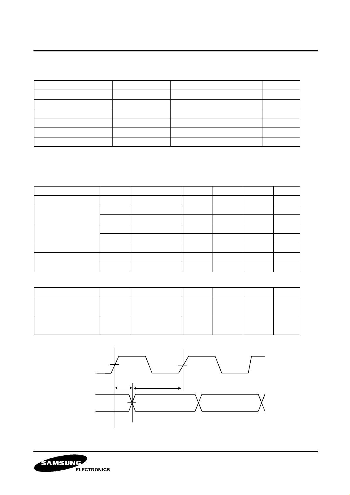
ABSOLUTE MAXIMUM RATINGS
Characteristics Symbol Value Unit
Supply Voltage V
Teminal input Voltage V
Power Dissipation P
DD
I
D
Operating Temperature TORR 0 ~ +70
Storage Temperature T
Latch-Up Current I
STG
LU
ELECTRICAL CHARACTERISTICS
DC
Characteristics Symbol Test Condition Min Typ Max Unit
Operating Voltage V
Input Voltage
output Voltage
Operating Current I
Maximum Input I
Leakage Current I
DD
V
IH
V
IL
V
OH
V
OL
DD
IH
IL
Ta = 25°C 4.75 5.0 5.25 V
Ta = 25°C 0.7V
Ta = 25°C - - 0.3V
IOH = -1mA 2.4 - - V
IOL = 1mA - - 0.4 V
V
= 5V - 140 160 mA
DD
VI = 0~V
VI = 0~V
DD
DD
-0.3 to 7 V
-0.3 to VDD +0.3 V
700 mW
-40 ~ +125
100 mA
DD
- - V
DD
-10 - 10
-10 - 10
°C
°C
V
µA
µA
AC
Characteristics Symbol Test Condition Min Typ. Max Unit
Input Data Setup Time
T
SU
VDD = 5±5%,
5
-
-
Ta = 0 ~70°C
Input Data Hold Time
T
HD
VDD = 5±5%,
5
-
50
Ta = 0 ~70°C
PCLK
CD9~0
T
HD
T
SU
nsec
nsec
VID-97-D004
February 1997
6
Page 7
KS7306 DIGITAL CAMERA PROCESSOR
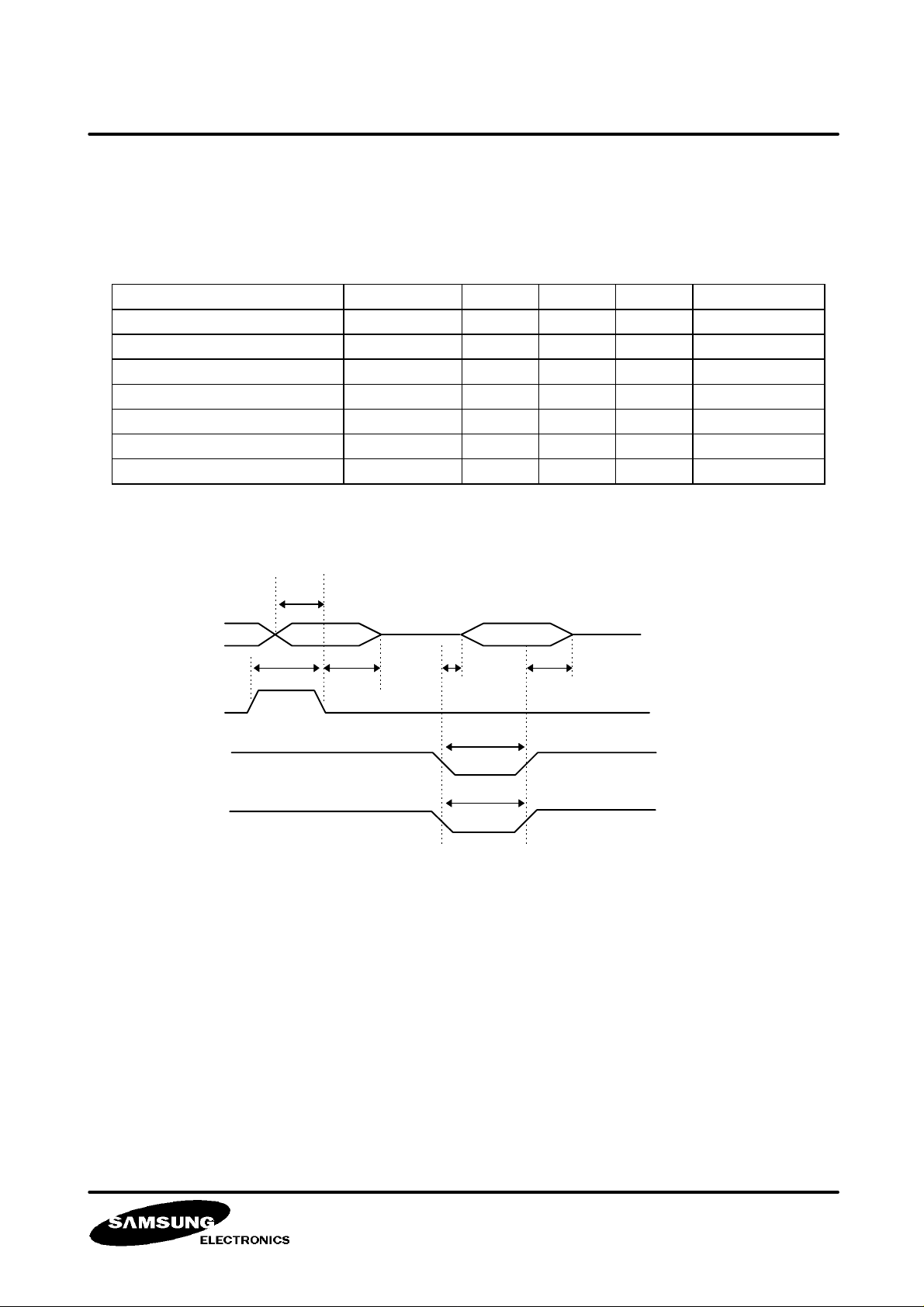
MICOM INTERFACE
1. NEC MICOM INTERFACE
Characteristics Symbol Min Typ Max Unit
Address setup time Tast 15 - - nsec
Address hold time That 35 - - nsec
AS pulse width Tasw 35 - - nsec
RDN pulse width Trdw 400 - - nsec
WRN pulse width Twrw 400 - - nsec
Data delay from RDN,WRN Td - - 100 nsec
Data hold time Tdh 0 - - nsec
MD7~0
AS
RDM
WRN
Tast
ADDR DATA
Tsaw
Taht
Td
Trdw
Twrw
Tdh
READ Mode
( WRN = ″1″)
WRITE Mode
( RDN = ″1″)
VID-97-D004
February 1997
7
Page 8
KS7306 DIGITAL CAMERA PROCESSOR
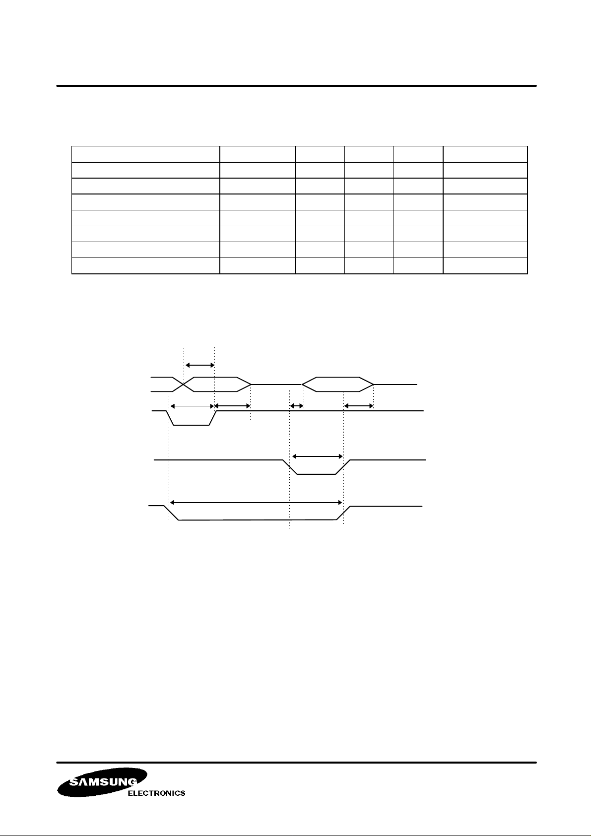
2. SAM8 MICOM INTERFACE
Characteristics Symbol Min Typ Max Unit
Address setup time Tast 15 - - nsec
Address hold time That 35 - - nsec
AS pulse width Tasw 35 - - nsec
RDN pulse width Trdw 400 - - nsec
WRN pulse width Twrw 400 - - nsec
Data delay from RDN,WRN Td - - 100 nsec
Data hold time Tdh 0 - - nsec
Tast
MD7~0
AS
RDM
WRN
ADDR DATA
Tsaw Taht
Twrw
Td Tdh
Trdw
READ Mode
( WRN = ″1″ )
WRITE Mode
( RDN = ″1″ )
VID-97-D004
February 1997
8
Page 9
KS7306 DIGITAL CAMERA PROCESSOR
SYSTEM DESCRIPTION
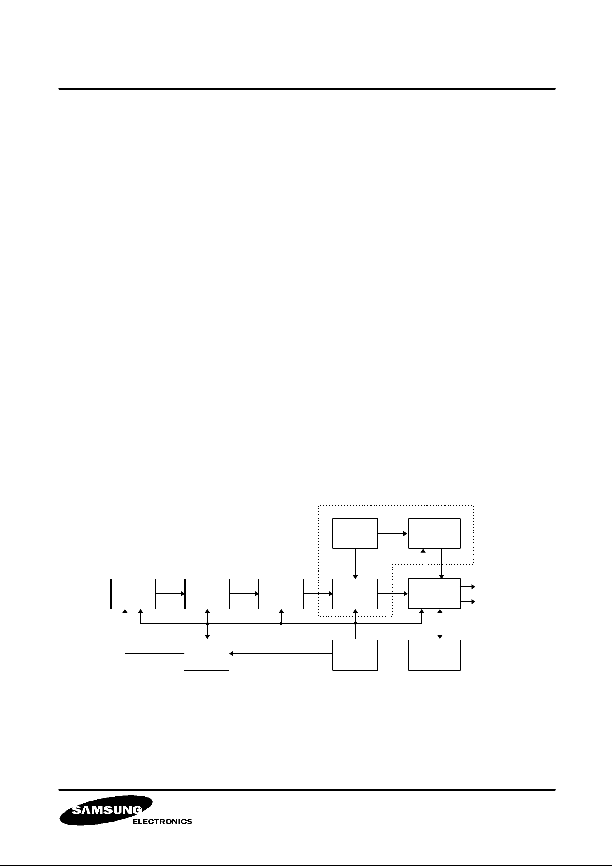
The video data output from CCD go through CDS IC (KA7307) and become quantized by 10 bit ADC.
For hand tremble correction in the CCD controlled gyro sensor method, the quatized video data are fed
to FCM in which effective pixel section of the data gets corrected and extended, then the data are
entered to the signal processor (KS7306) for YC coding so that the data are propely encoded to
conform with NTSC/PAL broadcasting method.
The encoded data is converted to analog signal by the built-in DAC and output Y.C signal finally.
The camera embodies current video status detection function needed for AE/AF/AWB function as an
automatic control provision of the camera system. The function of signal processing and video status
detection is implemented by data communication with the micom through the parallel interfaces to
allow setting of variable parameters, transmisson of detection signals, and reception of control signals
that are necessary in the signal processing. The clock used in IC' s is supplied by a separate IC, the
timining generator (KS7213). For the zooming, the Y,(R-Y)(B-Y) interface to the processing is
provided. And the interface allows interfacing with IC' s for the option of other digital effects.
The timing generator generates time pulse and video syncronizing signal required in all functional
block of the camera system. The clock supports the vertical expansion mode especially required in
CCD controlled gyro sensor and electronic zooming.
Using the clock furnished by the clock generator, the digital zoom (KS7314) performs zooming by
means of vertical interpolation of expanded CCD output and horizontal expansion and interpolation of
the output.
In this camera system, IC' s used for FCM, gyro, microcontroller, and DZ functions respectively are
the ones required only in the system that employs CCD controlled gyro sensor and electronic zooming
for optional funtions while a system pursuing electronic zooming alone requires employment of DZ IC
only to achieve the purpose. The CCDs of 510H (NTSC/PAL) and 760H (NTSC/PAL) allow a range of
system configurations that support 470K, 520K, and 620K (wobble correction CCD) pixels. The figure
below illustrates the camera system.
A/D; Analog to Digital
CCD; Charge Coupled Device
FCM; Frquency Converting Memory
DZ; Digital Camera Process
DCP; Digital Camera Process
CCD
CDS
KA7307
V-Driver
KS7221
A BLOCK DIAGRAM OF CAMERA SYSTEM CONFIGRATION
A/D
10bit
<OPTION>
Gyro
uCOM
FCM
KS7308
TG
KS7213
DZ
KS7314
DCP
KS7306
System
µCOM
Y
C
VID-97-D004
February 1997
9
Page 10
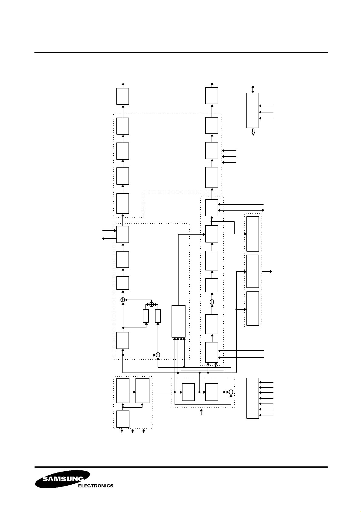
KS7306 DIGITAL CAMERA PROCESSOR
OPD- PROCESSOR
CD9 ~ 0
YI7 ~ 0
YO7 ~ 0
AY
ENCODER
AY
IF EFFECT SFC BM DAC
CSUP
HUE &
MD7 ~ 0
MICOM
INTERFACE
INT. REGISTER
BF
LALT
FSCA
UVO3 ~ 0
UVIO3 ~ 0
AWB
INTEGRATOR
WRN
RDN
AS
LPF γ DLY IF EFFECT BLK SYNC YDL DAC
Y PROCESSOR
DET
DEFECT
PREPROCESSOR
CLAMP
BLOCK DIAGRAM
PBLK
HAP
DEFECT
CORRECT
VSKIP
( - )
VAP
DET
HL / EDGE
LM
CDIFF
MATRIX
γ
W/B
RGB
MATRIX
B
/C
R
/C
LPF
L
Y
C PROCESSOR
LM
LHLD
AF ZONE
AE
INTEGRATOR
AF
INTEGRATOR
ID
HCON
TIMING
INTERFACE
HD
VD
PCLK
CBLK
CSYNC
RSTN
XCK
VID-97-D004
February 1997
10
Page 11
KS7306 DIGITAL CAMERA PROCESSOR
Y
OMDL
OMDH
OA2W1L
OA1W1L
OA2W1M
OA1W1M
OA1W2L
OA2W2L
OA1W2M
OA2W2M
OAP2W1L
OAP1W2L
OAP1W1L
OWN
OAP2W2L
OWSH
OACCL
16
OACCM
OA2W1H
OA1W1H
24
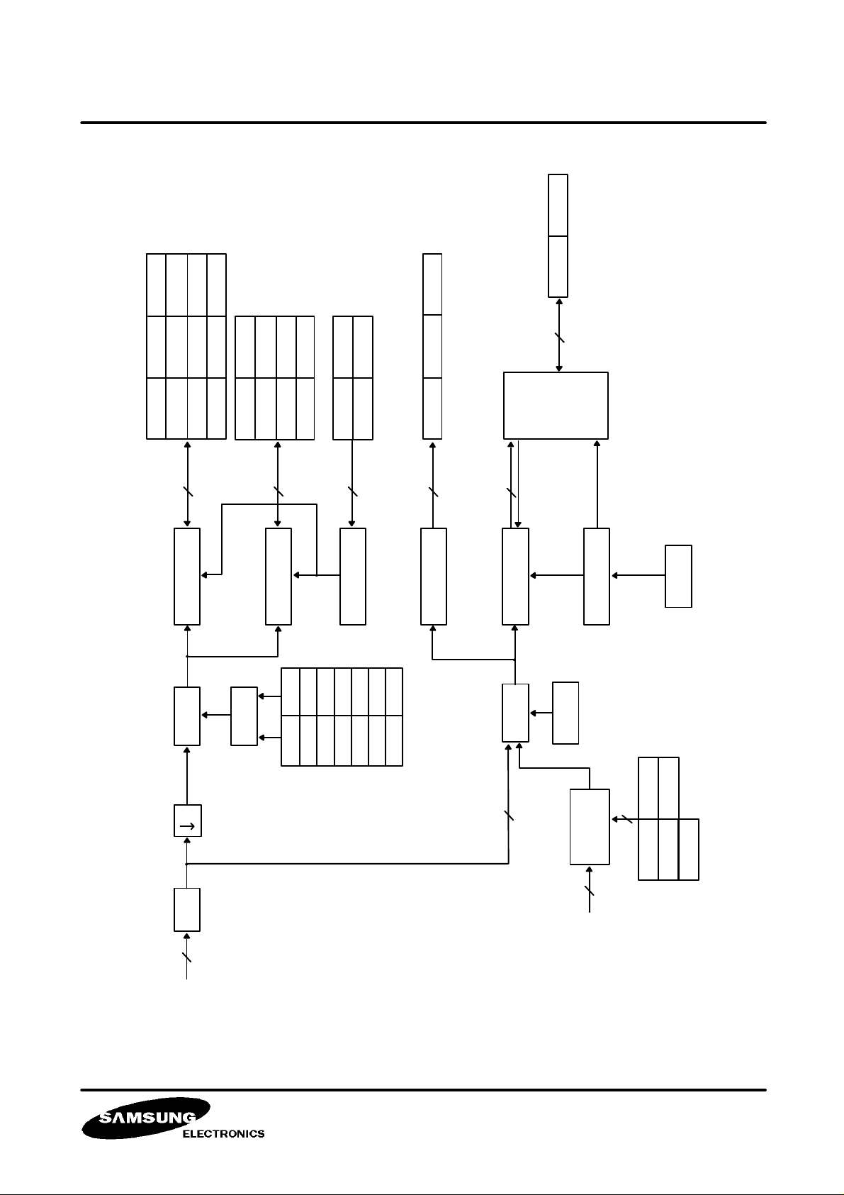
INTEGRATOR
HPF
2
OA1W2H
OA2W2H
OAP2W1H
OAP1W2H
OAP1W1H
16
Peak & Hold
MUX
OAP2W2H
OPC1A
OPC1B
OPC2B
OPC2A
OWM
OWSV
8
Window Control
OPC1E
OPC1C
OPC1D
OPC2E
OPC2C
OPC2D
OPC1F
OPC1G
OPC2F
OPC2G
OACCH
24
INTEGRATOR
Detection
16
INTEGRATOR
MUX
6
SRAM
Memory
(16b *48w)
OADR
Memory Control
OYL
6
OBYTH
OADR
LPF
8
OPD-PROCESSOR BLOCK DIAGRAM
VID-97-D004
February 1997
Comparator
6
(R-Y)/(B-Y)
OYH
OADS
ORYTH
11
Page 12
KS7306 DIGITAL CAMERA PROCESSOR
OPERATION OF BLOCKS
1. Preprocess
In case of signal processing of a camera with single CCD, before the performance of main processing,
it takes the optical black appearing before the real data among CCD data as the reference value and
the mean figure of it enables correct alignment of the black in the main processing, and in case of
defect found existing in CFA mode, it locates 4 errornous spots in maximum and processes to replace
the errors with two siding data by initial interpolation and then outputs line memory.
2. Line memory
Two built-in 10 bits line memories for 3 line color processing in 2H delay application, enable
simultaneous vision of 3 horizontal video lines, and in the processing of luminance signals, 1H delayed
signal, the H1D is offered, and in the chroma signal processing, HO2D or the luminance signal process
lines interpolated by two siding lines one in front and the other in the back are offered.
The line momory has 1024 depth for safe application to a CCD with 620 pixels, of 16:9 aspect.
For application to gyro sensor based and CCD controlled electronic image stabilizer system, it has the
functional capability to hold previous line at the blank signal line.
This is externally controlled by a LHLD signal.
3. Y processor
- LPF
The filter removes recurring pattern noise of single type CCD.
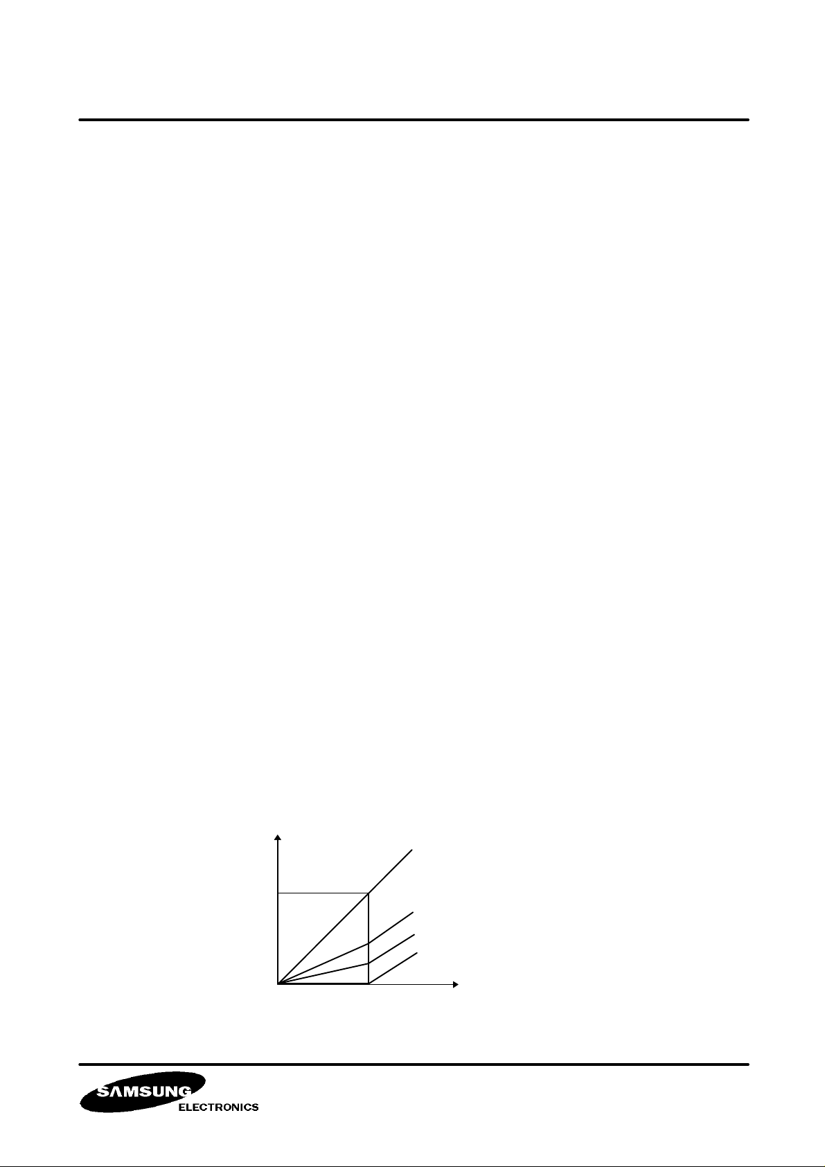
- Non-linear characteristics in H aperture application :
In order to reduce back noise caused by the noise of low luminance when H aperture is emphasized,
low luminance components are compressed before the aperture.
OUTPUT
BKG(X1)
BKG(X1/2)
BKTH
BKG(X1/4)
BKG(X0)
INPUT
VID-97-D004
February 1997
12
Page 13

KS7306 DIGITAL CAMERA PROCESSOR
- H_Aperture
Horizontal and vertical outline portions are emphasized.
INPUT
HAFS<1:0> = ″00″
HAFS<1:0> = ″01″
HAFS<1:0>= ″10″
HAFS<1:0> = ″11″
- REGISTER
HAPG : Horizontal Aperture Gain Control
5bits (X0 ~ X0.96875)
VAPG : Vertical Aperture Gain Control
5bits (X0 ~ X1.9375)
APSC : Aperture Slice Level
6bits (0~63)
APCLP : Aperture Clip Level
2bits 0 0 OFF
0 1 256
1 0 128
1 1 64
OUT
-APSC
IN
OUT
-APCLP
IN
APSC
< Noise Slice >
VID-97-D004
February 1997
APCLP
< Aperture Clip >
13
Page 14

KS7306 DIGITAL CAMERA PROCESSOR
- Gamma and knee
Adopting user defined variable gamma and knee in eight step piecewise linear method allows the user
free adjustment of the coefficient.
4. C-Processor
- S/H and interpolation LPF
With the input of HID and H02D signals from the line memory, C-Processor samples and holds S
and S2 for the generation of RGB chroma signals.
The band width of the signals so generated is limited by LPF.
- RGB matrix
Based on Cr, Cb and YC signals being the sum and balance components of S1 and S2, RGB chroma
signals are obtainable from the following matrix.
1
YC = S1 + S2, Cr = S2 - S1, Cb = S1 - S
2
R = Cr + CCOR X YC (or G)
G = YC - (Cr + Cb)
B = Cb + CCOB X G (or YC)
Register :
CCOR : Matrix coefficient for RED generation 6 bits (0-X0.25)
CCOB : Matrix coefficient for BLU generation 6 bits (0-X0.25)
CMATX : 2bits RED BLUE
0 0 Y
C
G
0 1 G G
1 0 G Y
1 1 YC Y
C
C
- White and black balance control :
Through interfacing with the micom, RB signal level is coordinated with G signal level.
Register :
* GWB : GREEN WHITE BALANCE CONTROL
8 bits (0~X4)
* RWB : RED WHITE BALANCE CONTROL
8 bits (0~X8)
* BWB : BLUE WHITE BALANCE CONTROL
8 bits (0~X8)
* GBLK : GREEN BLACK BALANCE CONTROL (2 ′S complement)
8 bits (-128 ~127)
* RBLK : RED BLACK BALANCE CONTROL (2 ′S complement)
8 bits (-128 ~127)
* BBLK : BLUE BLACK BALANCE CONTROL (2 ′S complement)
8 bits (-128 ~127)
VID-97-D004
February 1997
14
Page 15
KS7306 DIGITAL CAMERA PROCESSOR
- Gamma correction :
The process is indentical to the variable gamma method employed in the process of Y signals.
Register :
CGM1 - CGM8 : C-Gamma Y fraction coefficient
8 bits (0~255)
- Chroma MATRIX
It generates R-Y and B-Y signals of basic color space used as NTSC/PAL broadcast standards.
- HUE and gain control
Micro adjustment can be made to coordinate the balance vector to its complement color vector.
Individual adjustment against +, - on the R-Y and B-Y vector space that color regeneration is enhanced.
Register :
R-Y
RHPN
BHPN
(-1~X1)
RHNP
BHNP
(-1~X1)
RHPP
BHPP
(-1~X1)
B-Y
RHNN
BHNN
(-1~X1)
- Chroma suppress
It supresses false chroma signal by horizontal outline and high luminance signal.
Supress level is adjustable by the mode data.
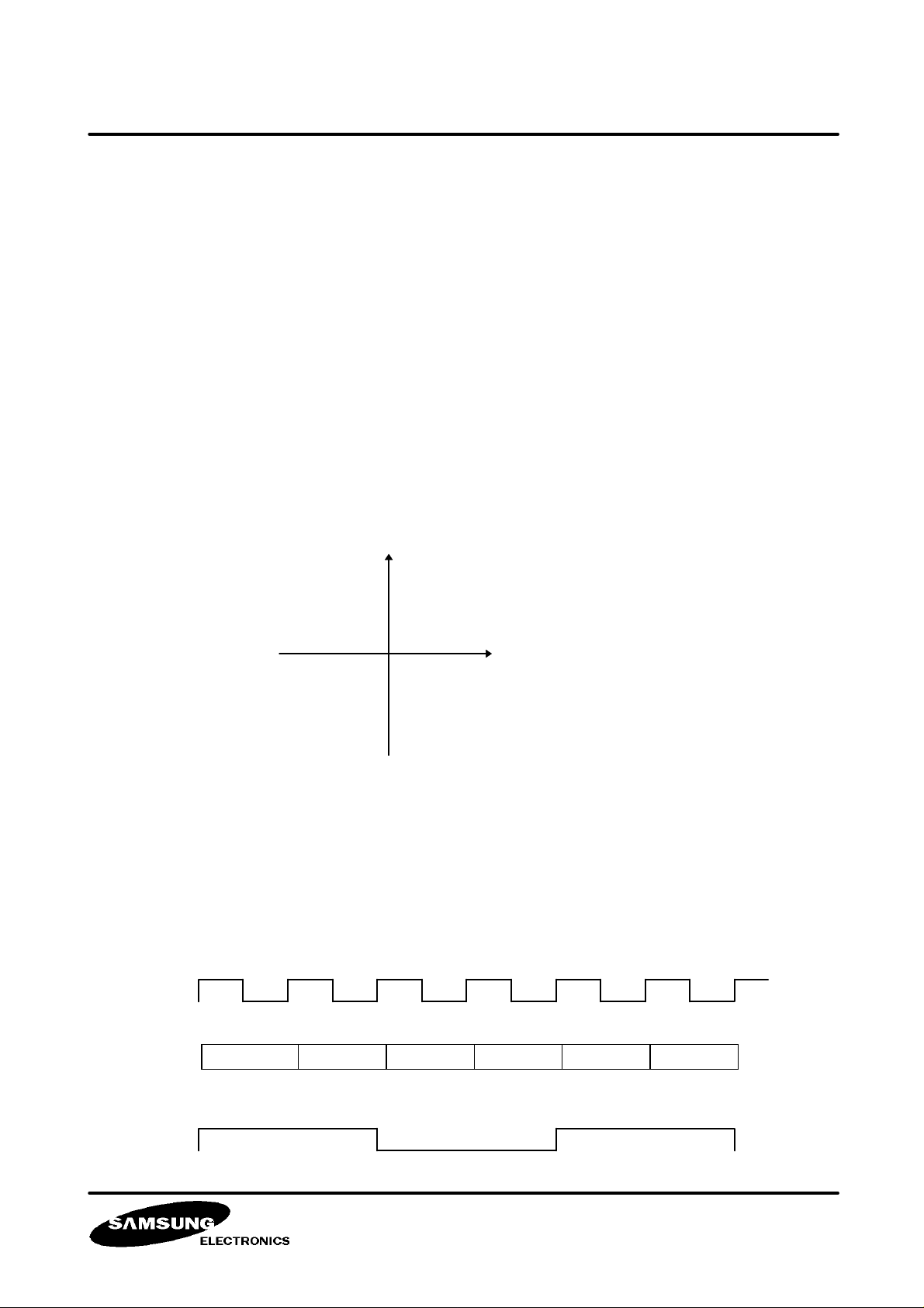
- Chroma signal interface
PLCK
UVO3 ~ 0
UVCK
..
RY0<7:4> RY0<3:0> BY0<7:4> BY0<3:0> RY1<7:4> RY1<3:0>
VID-97-D004
February 1997
.....
15
Page 16

KS7306 DIGITAL CAMERA PROCESSOR
5. NTSC/PAL encoder
- Digital effects
It performs various digital effects and Mosaic, Art Freeze, and Posi/Nega inversion.
Register :
. Art 3 bit 000:normal 001:128 rep val* 010:64 rep val* 011:32 rep val*
100:6 rep val* 101:8 rep val* 110:4 rep val* 111:2 rep val*
( *Rep val stands for representative value.)
. Nega 1 bit 0:normal 1:negative
- Fade function
A smooth screen shift is available by Y/C gain control (8bit resolution)
Register :
. Ygain 8bits 0-X1
. Cgain 8bits 0-X1
- Set-up and white clip
It determines the set-up level that conforms to specific broadcast method (NTSC/PAL) and defermins
also adequate white clip level.
Register :
. Set-up 5bits 0-32
. WCLP 8bits 0-256
- BLK/SYNC mix
CBLK/CSYNC are mixed to conform specific broadcast method
- Sampling frequency converter
The chroma signal synchronized to PCLK is converted to 4FSC frequency for chroma modulation.
- Modulation
The chroma data synchronized to 4FSC is put to repeat R-Y,B-Y in 2FSC frequncy,and invert in 4FSC
frequncy and thus modulation of chroma signal is achieved. In this process the level of burst signal
applied by the EUSC/EVSC reg, can be controlled and by the adjustment of EUSC/EVSC, color phase
can
be rotated entirely.
Register :
. EUSC 8bits B-Y burst level
. EVSC 8bits R-Y burst level
- Delay
The delays developed in the signal processing path of luminance and chroma signals are compensated
and other delicate delays resultant from the external applications can also be compensated.
VID-97-D004
February 1997
16
Page 17

KS7306 DIGITAL CAMERA PROCESSOR
* ORYTH
6. OPD Processor
The OPD Processor detects signals for AE/AF1/AF2/AWB and enters the detected signals to the
micom through the micom interface. The signals for AF1/AF2 can be detected simultaneously in one
filed for both of integral and peak values and the detection field can be set freely set by the user.
The peak value is, however, obtained by means of finding from a line in each field first and then
repeated by lines to fine the peak. The signals for AE/AWB can be detected by means of taking
integrated value of entire image or a sectional value of the image area divided in 48 sections.
Register :
* OCMD
* OA1W1H,OA1W1M,OA1W1L
* OA1W1H,OA1W1M,OA1W1L
* OA1W2H,OA1W2M,OA1W2L
* OA2W2H,OA2W2M,OA2W2L
* OAP1W1H,OAP1W1L
* OAP2W1H,OAP2W1L
* OAP1W2H,OAP1W2L
* OAP2W2H,OAP2W2L
* OACCH,OACCM,OACCL
* OMDH,OMDL
* OWM
* OWN
* OWSV
* OWSH
* OADR
- LPF; 6Tap FIR filter (-3db at 2 MHZ)
Signal band for input is limited for AE/AF.
- HPF; 3 Order IIR filter (HPF1:200KHZ, HPF2:600KHZ)
The filter suppresses low frequency components to enable detection of only the outline signal
selectively for AF1/AF2. Detection of AF1/AF2 is performed simultaneously for each horizontal line
that detection of AF1/AF2 singal in any one field is enabled.
The filter 3 order IIR filter is structured a hardware like, but coefficients are devised programmable
that the performance charactor can be adjusted by the user.
8 bits
8 bits * 3
8 bits * 3
8 bits * 3
8 bits * 3
8 bits * 2
8 bits * 2
8 bits * 2
8 bits * 2
8 bits * 3
8 bits * 2
8 bits
8 bits
8 bits
8 bts
6 bts
Mode settings command register
Integrated data of A area for AF1
Integrated data of A area for AF2
Integrated data of B area for AF1
Integrated data of B area for AF2
Peak data of A area for AF1
Peak data of A area for AF2
Peak data of B area for AF1
Peak data of B area for AF2
Peak data of full area for AE/AWB
Integrated of small image of sectioned area
Pixel number of small image of sectioned area
Line number of small image of sectioned area
Vertical start point of area A for AF
Horizontal start point of area A for AF
RAM start address (Write/Read)
Register :
* OPC2A, OPC2B, OPC2C, OPC2D, OPC2E, OPC2F, OPC2G 8bits AF2 HPF COEFFICIENTS
* OPC1A, OPC1B, OPC1C, OPC1D, OPC1E, OPC1F, OPC1G 8bits AF1 HPF COEFFICIENTS
- Comparator
It removes chroma signal from the high luminance and low luminance components in R-Y and B-Y signals
in order to limit the signal range suitable for input to AWB for the purpose of the signal detections.
Register
* OYH 6bits High luminance threshold level
* OYL 6bits Low luminance threshold level
* ORY? 6bits R-Y chroma signal threshold level
* ORYTH
* ORY? 6bits B-Y chroma signal threshold level
* ORBYTH 6bits (R-Y) + (B-Y) threshold level
VID-97-D004
February 1997
17
Page 18

KS7306 DIGITAL CAMERA PROCESSOR
7. Timing interface
It generates various clock as required in the inside of IC and performs delay adjust for various video
synchronizing signals and also the delay adjustment of final output of video synchronization signal.
8. Micom interface
A parallel interface is employed for transmission of information ever various parameters reqired in the
signal processing. And all sorts of commands and coefficients are either processed or set through the
port, and reading signal for detection of AE/AF/AWB.(For AE/AF/AWB detection, reading of signals
should be completed within VBLK process time.)
For the coefficients of fields, the write timing is enabled from the next field to alleviate the burden of
the micom.
In this instance, your attention is invited to the fact that if complete setting of coefficients that should
be set initially during the VBLK time is not accomplished, later setting will cause image instability.
Perimarily, parallel port interface is applicable to NEC series and SAM8 series micom.
9. D/A converter
The device contains two built-in channels of D/A converters for encoded luminance and chroma
signals.
VID-97-D004
February 1997
18
Page 19
KS7306 DIGITAL CAMERA PROCESSOR
THreshold value)
THreshold value)
for ODM)
Supress)
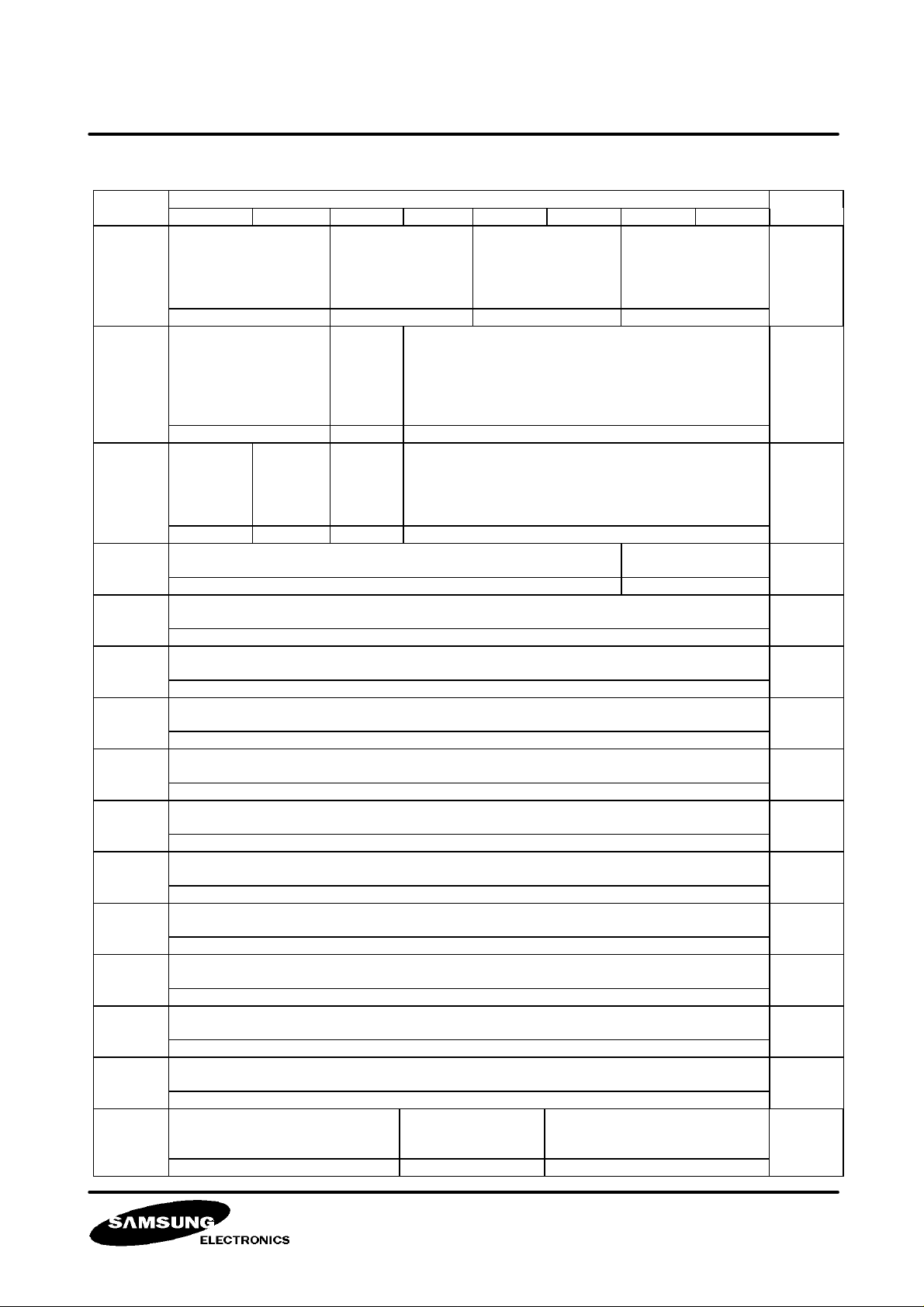
KS7306 MICOM REGISTER MAP
ADDR. USED
00H
01H
02H
O3H
04H
05H
06H
07H
08H
09H
0AH
0BH
0CH
0DH
0EH
D7 D6 D5 D4 D3 D2 D1 D0
YVBKTH<1:0>
(Vertical
BlacK noise
10(2H) 10(2H) 10(2H) 10(2H)
YHAFS<1:0>
(Horizontal Aperture
Filter Selection)
10(2H) 0(0H) 10000 (10H)
YSEL
(Y signal
SELect
1(1H) 1(1H) 1(1H) 10000 (10H)
(Y Process ART freeze effect for
YEGCS
(EdGe
Color
YART<2:0>
DVC mode)
000(0H) 00 (OH) 000 (OH)
YVBKG<1:0>
(Vertical BlacK
noise Gain)
YDVCN
EGA
(DVC
mode
NEGA
effect)
YHLCS
(High-
Light
Color
Supress)
YAPSC <5:0>
(APerture Slice Control)
000000 (00H) 10(2H)
(Y HighLight REFerence value for color supress) LUMA
(Y Edge REFerence value for color supress) LUMA
(Y Signal GamMa bending point 1) LUMA
(Y Signal GamMa bending point 2) LUMA
(Y Signal GamMa bending point 3) LUMA
(Y Signal GamMa bending Point 4) LUMA
(Y Signal GamMa bending Point 5) LUMA
(Y Signal GamMa bending Point 6) LUMA
(Y Signal GamMa bending point 7) LUMA
(Y Signal GamMa bending point 8) LUMA
DATA
YHBKTH<1:0>
BlacK noise
(Horizontal APerture Gain)
YHLREF <7:0>
10000000 (80H)
YEGREF <7:0>
00010000 (10H)
YGM1 <7:0>
00011100 (1CH)
YGM2 <7:0>
00100111 (27H)
YGM3 <7:0>
00110101 (35H)
YGM4 <7:0>
01001001 (49H)
YGM5 <7:0>
01100100 (64H)
YGM6 <7:0>
10001000 (88H)
YGM7 <7:0>
10111010 (BAH)
YGM8 <7:0>
11111111 (FFH)
YLPFSEL<1:0>
(Y process LPF
SELection)
(Horizontal
YHAPG<4:0>
YVAPG <4:0>
(Vertical APerture Gain) LUMA
(Color Supression coeff.
YHBKG<1:0>
(Horizontal BlacK
noise Gain)
YAPCLP<1:0>
(APerture CLiP) LUMA
YCSDLY<2:0>
DeLaY adjust)
LUMA
LUMA
LUMA
VID-97-D004
February 1997
19
Page 20
KS7306 DIGITAL CAMERA PROCESSOR
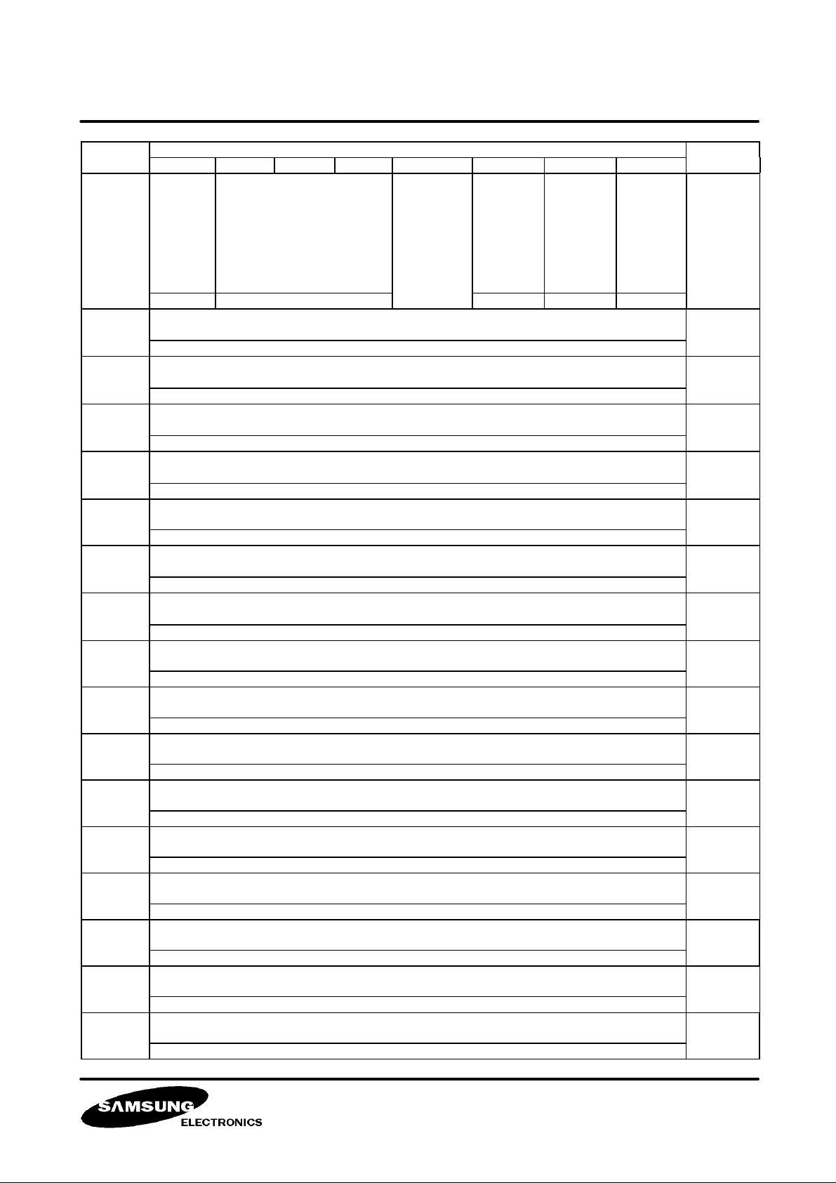
ADDR. USED
20H
21H
22H
23H
24H
25H
26H
27H
28H
29H
2AH
2BH
2CH
2DH
2EH
2FH
30H
D7 D6 D5 D4 D3 D2 D1 D0
CDVCN
EGA
(C
process
DVC
mode
NEGA
effect)
0(0H) 111(7H) 1(1H) 1(1H) 1(1H)
CLPFSEL
(Cr/Cb/Yl Signal
LPF Select)
CCORB<7:0> → CCOR<7:0>
(Color matrix Coeff. of Cr signal)
CCORB<7:0> → CCOB<7:0>
(Color matrix Coeff. of Cr signal)
CWBRB<7:0> → CWBR<7:0>
(Color White Balance coeff. of Cr signal)
CWBRB<7:0> → CWBB<7:0>
(Color White Balance coeff. of Cb signal)
(Color White Balance coeff. of G signal) CHROMA
CDSRB<7:0> → CDSR<7:0>
(Color Dark Slice coeff. of Cr signal)
CDSRB<7:0> → CDSB<7:0>
(Color Dark Slice coeff. Of Cb signal)
(Color Dark Slice coeff. Of G signal) CHROMA
(Chroma Signal Gamma bending Point 1) CHROMA
(Chroma Signal Gamma bending Point 2) CHROMA
(Chroma Signal Gamma bending Point 3) CHROMA
(Chroma Signal Gamma bending Point 4) CHROMA
(Chroma Signal Gamma bending Point 5) CHROMA
(Chroma Signal Gamma bending Point 6) CHROMA
(Chroma Signal Gamma bending Point 7) CHROMA
(Chroma Signal Gamma bending Point 8) CHROMA
DATA
Not Used
01100111 (67H)
01100111 (67H)
00101000 (28H)
01000011 (43H)
CWBG<7:0>
00100000 (20H)
00000000 (00H)
00000000 (00H)
CDSG <7:0>
00000000 (00H)
CGY1 <7:0>
00011100 (1CH)
CGY2 <7:0>
00100111 (27H)
CGY3 <7:0>
00110101 (35H)
CGY4 <7:0>
01001001 (49H)
CGY5 <7:0>
01100100 (64H)
CGY6 <7:0>
10001000 (88H)
CGY7 <7:0>
10111010 (BAH)
CGY8 <7:0>
11111111 (FFH)
CYLS
(Yl
Signal
Gen..
Select)
CRMS
(Cr
Signal
Matrix
Select)
CBMS
(Cb
Signal
Matrix
Select)
CHROMA
CHROMA
CHROMA
CHROMA
CHROMA
CHROMA
CHROMA
VID-97-D004
February 1997
20
Page 21

KS7306 DIGITAL CAMERA PROCESSOR
DETECT
DETECT
ADDR.
31H
32H
33H
34H
35H
36H
37H
38H
39H
3AH
3BH
3CH
3DH
3EH
3FH
E0H
40H
41H
DATA
D7 D6 D5 D4 D3 D2 D1 D0
CRRGP <7:0>
(Cr(R-G) signal Positive gain) CHROMA
01011001 (59H)
CRRGN <7:0>
(Cr(R-G) signal Negative gain) CHROMA
0101001 (59H)
CRBGP <7:0>
(Cr(B-G) signal Positive gain) CHROMA
11110010 (F2H)
CRBGN <7:0>
(Cr(B-G) signal Negative gain) CHROMA
11110010 (F2H)
CBRGP <7:0>
(Cb(R-G) signal Positive gain) CHROMA
11011001 (D9H)
CBRGN <7:0>
(Cb(R-G) signal Negative gain) CHROMA
11011001 (D9H)
CBBGP <7:0>
(Cb(R-G) signal Positive gain) CHROMA
01110010 (72H)
CBBGN <7:0>
(Cb(B-G) signal Negative gain) CHROMA
01110010 (72H)
CRGP <7:0>
(Color difference signal (R-Y) Positive gain) CHROMA
01000000 (40H)
CRGN <7:0>
(Color difference signal (R-Y) Negative gain) CHROMA
01000000 (40H)
CRHP <7:0>
(Color difference signal (R-Y) Hue control Positive gain) CHROMA
00000000 (00H)
CRHN <7:0>
(Color difference signal (R-Y) Hue control Negative gain) CHROMA
00000000 (00H)
CBGP <7:0>
(Color difference signal (B-Y) Positive gain) CHROMA
01000000 (40H)
CBGN <7:0>
(Color difference signal (B-Y) Negative gain) CHROMA
01000000 (40H)
CBHP <7:0>
(Color difference signal (B-Y) Hue control Positive gain) CHROMA
00000000 (00H)
CBHP <7:0>
(Color difference signal (B-Y) Hue control Negative gain) CHROMA
00000000 (00H)
OA112 <7:0>
(ODM HFP coeff. A11 for AF2)
01101011 (6BH)
OA212 <7:0>
(ODM HPF coeff. A21 for AF2)
01110011 (73H)
USED
OPT_
OPT_
VID-97-D004
February 1997
21
Page 22

KS7306 DIGITAL CAMERA PROCESSOR
DETECT
DETECT
DETECT
DETECT
DETECT
DETECT
DETECT
DETECT
DETECT
DETECT
DETECT
DETECT
DETECT
DETECT
DETECT
DETECT
DETECT
DETECT
ADDR.
42H
43H
44H
45H
48H
49H
4AH
4BH
4CH
4DH
4EH
50H
51H
52H
53H
54H Not Used
55H Not Used
56H Not Used
D7 D6 D5 D4 D3 D2 D1 D0
DATA
OA222 <7:0>
(ODM HPF coeff. A22 for AF2)
10010101 (95H)
OB102 <7:0>
(ODM HPF coeff. B10 for AF2)
0110101 (75H)
OB202 <7:0>
(ODM HPF coeff. B20 for AF2)
01111011 (7BH)
OB212 <7:0>
(ODM HPF coeff. B21 for AF2)
10000110 (86H)
OCMD <7:0>
(ODM Command)
00000000 (00H)
OA111 <7:0>
(ODM HPF coeff. A11 for AF1)
01001010 (4AH)
OA211 <7:0>
(ODM HPF coeff. A21 for AF1)
01010100 (54H)
OA221 <7:0>
(ODM HPF coeff. A22 for AF1)
10110010 (B2H)
OB101 <7:0>
(ODM HPF coeff. B10 for AF1)
01100101 (65H)
OB201 <7:0>
(ODM HPF coeff. B20 for AF1)
01100101 (65H)
OB211 <7:0>
(ODM HPF coeff. B21 for AF1)
10100001 (A1H)
OW1SH <7:0>
(ODM Horizontal Start point of Window1 for AF)
01010100 (54H)
OW1EH <7:0>
(ODM Horizontal End point of Window1 for AF)
10100100 (A4H)
OW1SV <7:0>
(ODM Vertical Start point of Window1 for AF)
00101010 (2AH)
OW1EV <7:0>
(ODM Vertical End point of Window1 for AF)
01010010 (52H)
OAETH <5:0>
(ODM AE mode THreshold vaiue)
000000 (00H)
OYH_AE <5:0>
(ODM Y signal Upper threshold value of AE mode)
111111 (3FH)
OYL_AE <5:0>
(ODM Y signal Lower threshold value of AE mode)
000000 (00H)
USED
OPT_
OPT_
OPT_
OPT_
OPT_
OPT_
OPT_
OPT_
OPT_
OPT_
OPT_
OPT_
OPT_
OPT_
OPT_
OPT_
OPT_
OPT_
VID-97-D004
February 1997
22
Page 23
KS7306 DIGITAL CAMERA PROCESSOR
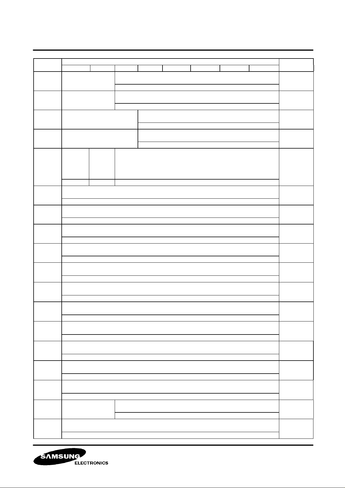
DETECT
DETECT
DETECT
DETECT
DETECT
DETECT
DETECT
DETECT
DETECT
DETECT
DETECT
DETECT
DETECT
DETECT
DETECT
DETECT
DETECT
DETECT
ADDR.
57H Not Used
58H Not Used
59H Not Used
5AH Not Used
5BH
5CH
5DH
5EH
5FH
60H
61H
62H
63H
64H
65H
66H
68H Not Used
69H
D7 D6 D5 D4 D3 D2 D1 D0
OHPF1E
N(ODM
HPF1
Enable
signal)
0(0H) 0(0H) 001111 (0FH)
OAREA
(OCMP
AREA)
DATA
OYH_AWB<5:0>
(ODM Y signal upper threshold value of AWB mode)
111111 (3FH)
OYL_AWB <5:0>
(ODM Y signal Lower threshold value of AWB mode)
000000 (00H)
ORYTH <4:0>
(ODM R-Y signal THreshold value of AWB mode)
11111 (1FH)
OBYTH <4:0>
(ODM B-Y signal THreshold value of AWB mode)
11111 (1FH)
ORBYTH <5:0>
(ODM (R-Y)+(B-Y) signal THreshold value of AWB mode)
OW2SH <7:0>
(ODM Horizontal Start point of Window2 for AF)
00000100 (04H)
OW2EH <7:0>
(ODM Horizontal End point of Window2 for AF)
11110010 (F2H)
OW2SV<7:0>
(ODM Vertical Start point of Window2 for AF)
00000010 (02H)
OW2EV <7:0>
(ODM VERTICAL End point of Window2 for AF)
01110111 (77H)
OAWO <23:16> → OA1W1H <7:0>
(ODM AF1 accumulation result of Window1)
00000000 (00H)
OAWO <7:0> → OA2W1L <7:0>
(ODM AF2 accumulation result of Window1)
00000000 (00H)
OAWO <15:8> → OA2W1M <7:0>
(ODM AF2 accumulation result of Window1)
00000000 (00H)
OAWO <23:16> → OA2W1H <7:0>
(ODM AF2 accumulation result of Window1)
00000000 (00H)
OAWO <7:0> → OA1W2L<7:0>
(ODM AF1 accumulation result of Window2)
00000000 (00H)
OAWO <15:8> → OA1W2M <7:0>
(ODM AF1 accumulation result of Window2)
00000000 (00H)
OAWO <23:16>→ OA1W2H <7:0>
(ODM AF1 accumulation result of Window2)
00000000 (00H)
OADR <5:0>
(ODM loadable RAM ADDRess)
000000 (00H)
OMDO <7:0> → OMDL <7:0>
(ODM RAM Data)
00000000 (00H)
USED
OPT_
OPT_
OPT_
OPT_
OPT_
OPT_
OPT_
OPT_
OPT_
OPT_
OPT_
OPT_
OPT_
OPT_
OPT_
OPT_
OPT_
OPT_
VID-97-D004
February 1997
23
Page 24
KS7306 DIGITAL CAMERA PROCESSOR
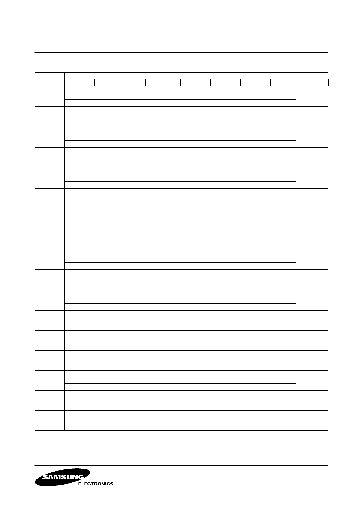
DETECT
DETECT
DETECT
DETECT
DETECT
DETECT
DETECT
DETECT
DETECT
DETECT
DETECT
DETECT
DETECT
DETECT
DETECT
DETECT
DETECT
ADDR.
6AH
6BH
6CH
6DH
6EH
6FH
70H Not Used
71H Not Used
D7 D6 D5 D4 D3 D2 D1 D0
DATA
OMDO <15:8> → OMDH <7:0>
(ODM RAM Data)
00000000 (00H)
OMCCO <7:0> → OACCL <7:0>
(ODM AE/AWB ACCumulation result)
00000000 (00H)
OMCCO <15:8> → OACCM<7:0>
(ODM AE/AWB ACCumulation result)
00000000 (00H)
OMCCO <23:16> → OACCL <7:0>
(ODM AE/AWB ACCumulation result)
00000000 (00H)
OAWO <7:0> → OA1W1L <7:0>
(ODM AF1 ACCumulation result of Window1)
00000000 (00H)
OAWO <15:8> → OA1W1M <7:0>
(ODM AF1 ACCumulation result of Window1)
00000000 (00H)
OWV <5:0>
(ODM Vertical subwindow Width of AE/AWB window)
011100 (1CH)
OWH <4:0>
(ODM Hor. subwindow Width of AE/AWB window)
USED
OPT_
OPT_
OPT_
OPT_
OPT_
OPT_
OPT_
OPT_
77H
78H
79H
7AH
7BH
7CH
7DH
7EH
7FH
OAWO <7:0> → OA2W2L <7:0>
(ODM AF2 accumulation result of Window2)
00000000 (00H)
OAWO <15:8> → OA2W2M <7:0>
(ODM AF2 accumulation result of Window2)
00000000 (00H)
OAWO <23:16> → OA2W2H <7:0>
(ODM AF2 accumulation result of Window2)
00000000 (00H)
OAP1W1 <7:0>
(ODM Peak hold for AF1 of Window1)
00000000 (00H)
OAP2W1 <7:0>
(ODM Peak hold for AF2 of Window1)
00000000 (00H)
OAP1W2 <7:0>
(ODM Peak hold for AF1 of Window2)
00000000 (00H)
OAP2W2 <7:0>
(ODM Peak hold for AF2 of Window2)
00000000 (00H)
OWSV <7:0>
(ODM Vertical subwindow Start point of AE/AWB window)
00111110 (3EH)
OWSH <7:0>
(ODM Horizontal subwindow Start point of AE/AWB window)
00000110 (06H)
OPT_
OPT_
OPT_
OPT_
OPT_
OPT_
OPT_
OPT_
OPT_
VID-97-D004
February 1997
24
Page 25
KS7306 DIGITAL CAMERA PROCESSOR
ADDR.
80H
81H
82H
83H
84H
85H
86H
87H
88H
89H
90H
91H
92H
93H
94H
DATA
D7 D6 D5 D4 D3 D2 D1 D0
Not
Used
POBSEL
(Optical
Black
data
SELection)
PDETEC
T1
(Defect
enable 1)
PDETEC
T2
(Defect
enable 2)
PCORR
ECT
(Defect
CORRE
CTion
enable)
0(0H) 0(0H) 0(OH) 0(0H) 0(0H)
PDEFECT_ TH <7:0>
(Preprocess DEFECT THreshold value)
00000000 (00H)
Not
Used
PHCNT_REF
<9:8>
00(0H)
PHCNT_REF <7:0>
(Preprocess Horizontal CouNT REFerence value)
00000000 (00H)
PVCNT_REF <7:0>
(Preprocess Vertical CouNT REFerence value)
00000000 (00H)
PHSTART<3:0>
(Preprocess defect detection Horizontal
START point)
(Preprocess defect detection Vertical START
PVSTART<3:0>
point)
0000(0H) 0000(0H)
PCLP_START<7:0>
(Preprocess digital Clamp optical black START point)
00000000 (00H)
Not
Used
POB_MICOM
<9:8>
00(0H)
POB_MICOM<7:0>
(Preprocess optical black data from MICOM)
00000000 (00H)
PSG_ODD_POS<3:0>
(Preprocess SG pulse ODD field
POSition)
PSG_EVEN_POS<3:0>
(Preprocess SG pulse EVEN field
POSition)
0000(0H) 0000(0H)
PA1 <7:0>
(Preprocess defect address 1)
00000000 (00H)
PA1 <15:8>
00000000 (00H)
Not
Used
PB1<2:0> Not
Used
PA1<18:16> PRE
000(0H) 000(0H)
PA2
(Preprocess defect address 2)
00000000 (00H)
PA2
00000000 (00H)
PDCLA
MP
(Digital
CLAMP
enable)
USED
PRE
PROCESS
PRE
PROCESS
PRE
PROCESS
PRE
PROCESS
PRE
PROCESS
PRE
PROCESS
PRE
PROCESS
PRE
PROCESS
PRE
PROCESS
PRE
PROCESS
PRE
PROCESS
PRE
PROCESS
PROCESS
PRE
PROCESS
PRE
PROCESS
VID-97-D004
February 1997
25
Page 26
KS7306 DIGITAL CAMERA PROCESSOR
ADDR.
95H
96H
97H
98H
99H
9AH
9BH
AOH
A1H
A2H
A3H
A4H
A5H
A6H
A7H
DATA
D7 D6 D5 D4 D3 D2 D1 D0
Not
Used
Not
Used
Not
Used
ENP
(Encoder
Nega/Po
si effect)
0(0H) 000(0H) 0000(0H)
EDZCBLK
OFF
(Encoder
DZ mode
CBLK
OFF)
0(0H) 00000(00H)
PB2<2:0> Not
Used
000(0H) 000(0H)
PA3
(Preprocess defect address 3)
00000000 (00H)
PA3
00000000 (00H)
PB3<2:0> Not
Used
000(0H) 000(0H)
PA4
(Preprocess defect address 4)
00000000 (00H)
PA4
00000000 (00H)
PB4<2:0> Not
Used
000(0H) 000(0H)
EART <2:0>
(Encoder ARTfreeze
Effect)
EYGAIN <7:0>
(Encoder Y signal GAIN) ENCODER
10110000 (BOH)
ECGAIN <7:0>
(Encoder Color signal GAIN) ENCODER
01001000 (48H)
Not Used
EWC <7:0>
(Encoder White Clip Control) ENCODER
11001000 (C8H)
EBLK <7:0>
(Encoder luminance BLanK Level) ENCODER
00111111 (3FH)
EUSC <7:0>
(Encoder U(B-Y) Signal burst level Control) ENCODER
00011111 (1FH)
EVSC <7:0>
(Encoder V(R-Y) Signal burst level Control) ENCODER
00011111 (1FH)
(Encoder Y signal DeLay control
(Encoder luminance set-up level)
EYDL <3:0>
ESU
PA2 PRE
PA3 PRE
PA4 PRE
selection)
USED
PROCESS
PRE
PROCESS
PRE
PROCESS
PROCESS
PRE
PROCESS
PRE
PROCESS
PROCESS
ENCODER
ENCODER
VID-97-D004
February 1997
26
Page 27
KS7306 DIGITAL CAMERA PROCESSOR
ADDR.
USED
DATA
D7 D6 D5 D4 D3 D2 D1 D0
EMBCK_
SEL
A8H
A9H Not
FAH
FBH
FCH
FDH
FEH
FFH
(Encoder
BM
clock
EDLY_SEL <3:0>
(Encoder DeLaY Selection)
EBFDLY <2:0>
(Encoder BF Delay
Selection)
SELection)
0(0H) 0000 (0H) 00 (0H)
Used
FSC_CO
NT
(FSC
Control)
FSC2_
CONT
(FSC2
Control)
FSC_R
selectio
0(0H) 0(0H) 0(0H)
Not
Used
(Delay Control Selection)
S1 <3:0>
0000(0H)
Not
Used
(Delay Control Selection)
S2 <5:0>
000000(00H)
TSTCMD <7:0>
(TeST ComManD)
00000000 (00H)
FCM
(FCM
mode)
Not
Used
HSYNCS <2:0>
(H SYNC pulse delay
Selection)
Not Used MICOM_
0 (0H) 000 (0H)
LALT-
CONT
(LALT
signal
CONTrol)
XCK-
CONT
(External
Clock
control
for
kasan)
Not
Used
MPCKS
EL
(Multi-
Media
selection)
HSEL
(Horizontal
selection)
VSEL
(Vertical
selection)
SCK_
CONT
(S-ClocK
control)
0 (0H) 0 (0H) 0 (0H) 0 (0H) 0 (0H) 0 (0H) 0 (0H)
SYNCHSH
(SYNC
wave
SHape)
Not
Used
C422
(4:2:2
mode)
WIDE
(WIDE
mode)
OLPFSEL
(LPF
selection
for ODM)
PAL
(PAL
mode)
HI8
(HIband
8mm
mode)
0 (0H) 0 (0H) 0 (0H) 0 (0H) 0 (0H) 0 (0H) 0 (0H)
N
_SEL
(FSC
Reset
n)
UVCK_
CONT
(UV-
ClocK
control)
DZ
(Digital
zoom
mode)
ENCOD
ER
ENCOD
ER
DLYCO
NT
DLYCO
NT
MICOM_
IF
IF
MICOM_
IF
MICOM_
IF
VID-97-D004
February 1997
27
Page 28
KS7306 DIGITAL CAMERA PROCESSOR
1. ADDRESS 00
1) YVBKTH <1:0> : Vertical Black noise THreshold value
- DATA <7:6>
2) YVBKG <1:0> : Vertical Black noise Gain
- DATA <5:4>
3) YHBKTH <1:0> : Horizontal Black noise THreshold value
- DATA <3:2>
4) YHBKG <1:0> : Horizontal Black noise Gain
- DATA <1:0>
OUTPUT
2. ADDRESS 01
1) YHAFS <1:0> : Horizontal Aperture Filter Selection
- DATA <7:6>
2) YDVCNEGA: Y process DVC mode NECA effect
- DATA <5>
YDVCNEGA = ″0″
YDVCNEGA = ″1″
3) YHAPG <4:0> : Horizontal APerture Gain
- DATA <4:0>
- RANGE : x0 ~ x0.96875
- FORMAT : 0.xxxxx
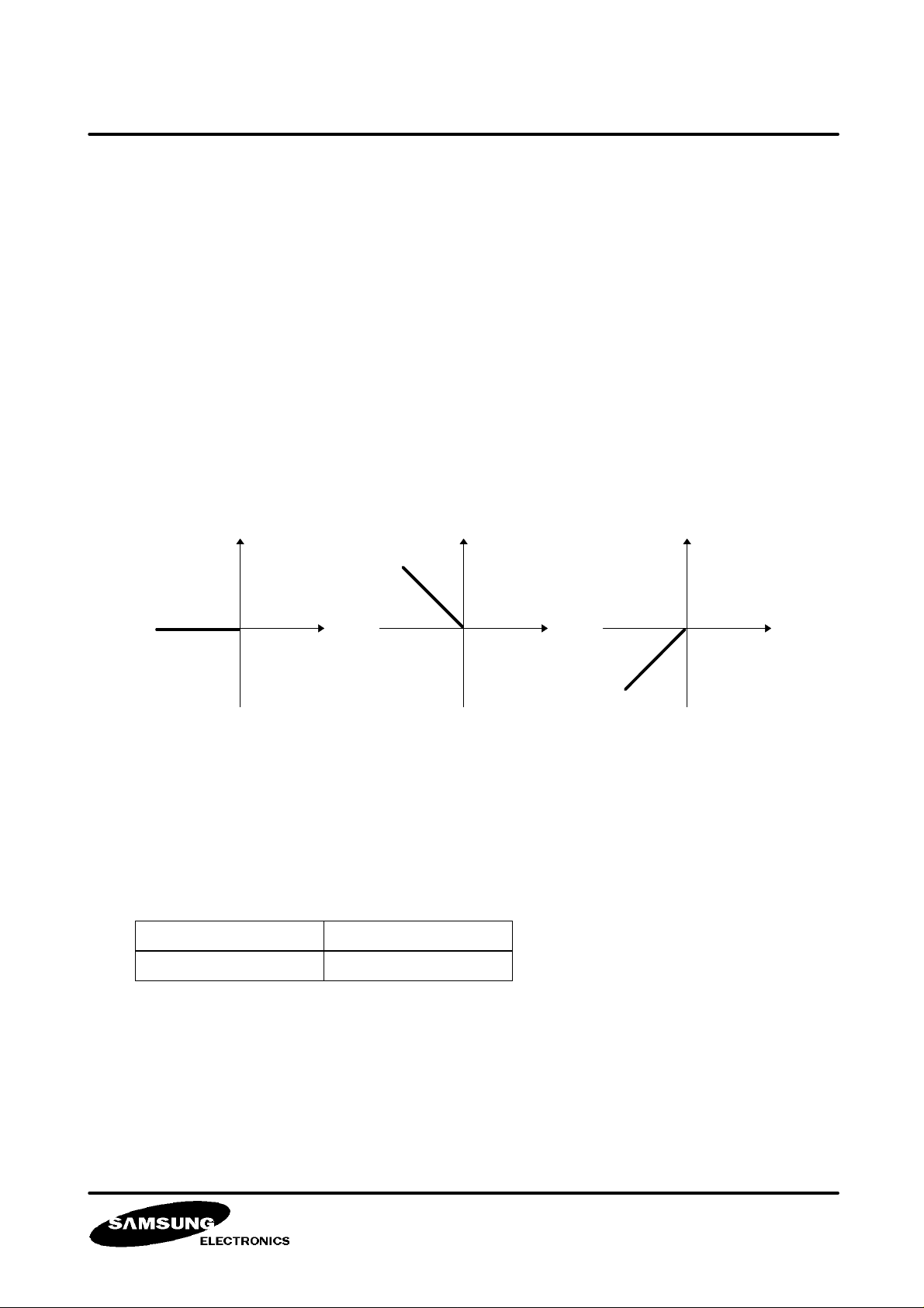
Normal operation(POSI)
Level conversion(NEGA)
BKTH
BKG(X1)
BKG(X1/2)
BKG(X1/4)
BKG(X0)
INPUT
3. ADDRESS 02
1) YSEL : Y signal SELection for OPT_DETECT
- DATA <7>
- OYSEL = ″0″ : Line Memory output is input to OPT-DEFECT Block that passed LPF.
OYSEL = ″1″ : Line Memory output is input directly to OPE-DEFECT Block.
2) YEGCS : EdGe Color Supress
- DATA <6>
3) YHILCS : HighLight Color Supress
- DATA <5>
VID-97-D004
February 1997
28
Page 29

KS7306 DIGITAL CAMERA PROCESSOR
EGCS HLCS SELECT
00
01 HighLight Coeff.
10 Edge Coeff.
IF(HighLight Coeff. > Edge Coeff.
⇒ HighLight Coeff.
11
4) YVAPG <4:0> : Vertical APerture Gain
- DATA <4:0>
- RANGE : X0 ~ X1.9375
- FORMAT : X.XXXX
ELSE
⇒ Edge Coeff.
4. ADDRESS 03
1) YAPSC <5:0> : APerture Slice Control
- DATA <7:2>
- RANGE : 0 ~ 31
2) YAPCLP <1:0> : APerture CLiP
- DATA <1:0>
″000″
5. ADDRESS 04
1) YHLREF <7:0> : Y HighLight REFerence for Color Supress
- DATA <7:0>
- IF (Y <YHLREF) ⇒ HighLight Coeff. = ″000″
- ELSE ⇒ HighLight Coeff. = ″000″ ~ ″111″
6. ADDRESS 05
1) YEGREF <7:0> : Y EdGe REFerence for color Supress
- DATA <7:0>
- IF (Y <YEGREF) ⇒ Edge Coeff. = ″000 ″
- ELSE ⇒ Edge Coeff. = ″000 ″ ~ ″111″
7. ADDRESS 06
1) YGM1 <7:0> : Y signal GamMa coeff.1
- DATA <7:0>
8. ADDRESS 07
1) GM2 <7:0> : Y signal GamMa coeff.2
- DATA <7:0>
VID-97-D004
February 1997
29
Page 30
KS7306 DIGITAL CAMERA PROCESSOR
52627
8
9
10
3
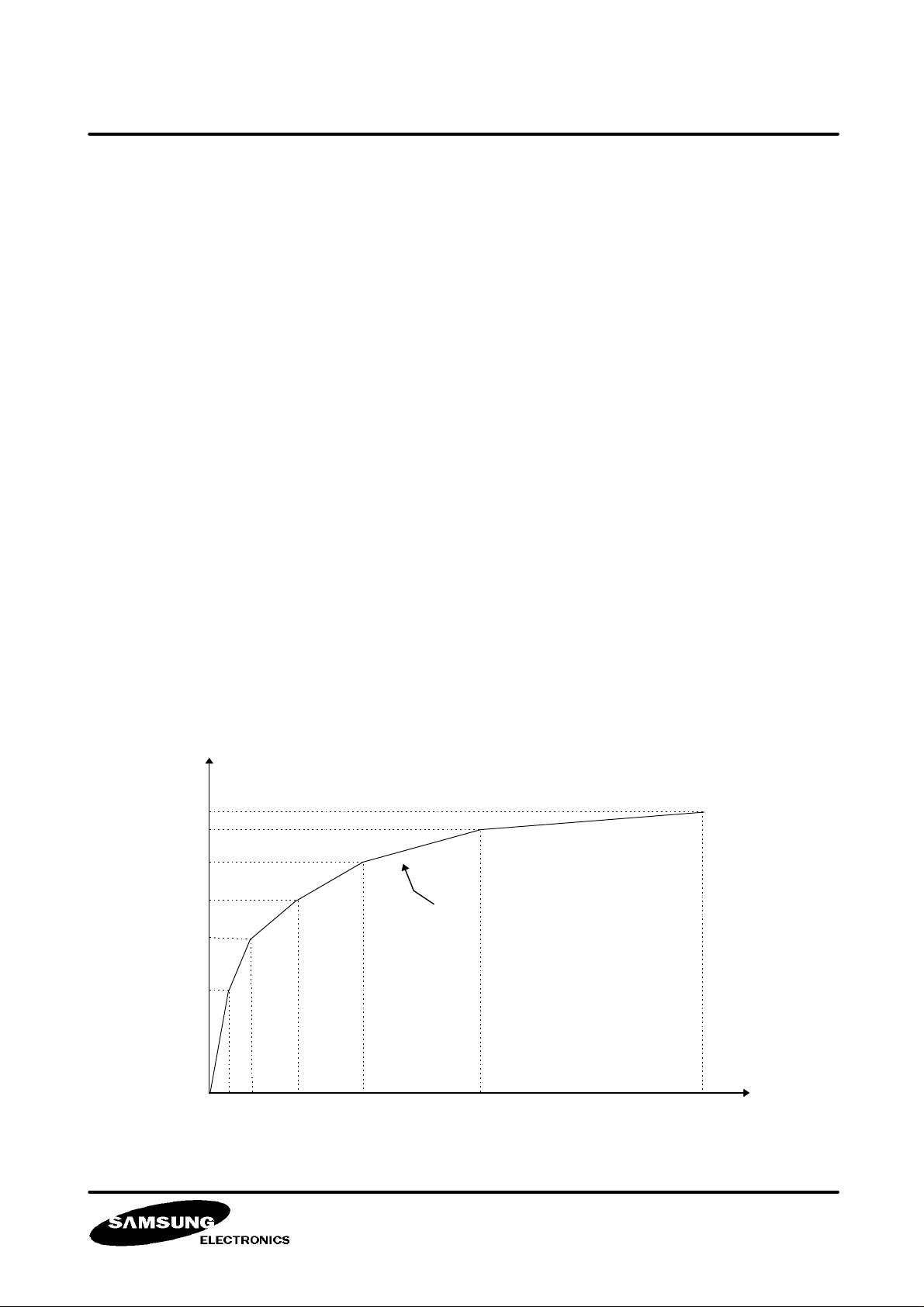
9. ADDRESS 08
1) YGM3 <7:0> : Y signal GamMa coeff.3
- DATA <7:0>
10. ADDRESS 09
1) YGM4 <7:0> : Y signal GamMa coeff.4
- DATA <7:0>
11. ADDRESS 0A
1) YGM5 <7:0> : Y signal GamMa coeff.5
- DATA <7:0>
12. ADDRESS 0B
1) YGM6 <7:0> : Y signal GamMa coeff.6
- DATA <7:0>
13. ADDRESS 0C
1) YGM7 <7:0> : Y signal GamMa coeff.7
- DATA <7:0>
14. ADDRESS 0D
1) YGM8 <7:0> : Y signal GamMa coeff.8
- DATA <7:0>
GOUT<7:0>
GY8<7:0>
GY7<7:0>
GY6<7:0>
GY5<7:0>
GY4<7:0>
GY3<7:0>
GY2<7:0>
X
Y
GY1<7:0>
GIN<9:0>
2
∗ GY1<7:0> : 2
2
4
<Gamma Chracteristic Curve>
2
VID-97-D004
2
30
February 1997
Page 31

KS7306 DIGITAL CAMERA PROCESSOR
15. ADDRESS 0E
1) YART<2:0>: Y signal ART freeze effect for DVC mode
- DATA <7:5>
YART<2><1><0> OPERATION YART<2><1><0> OPERATION
0 0 0 256 Level 1 0 0 16 Level
0 0 1 128 Level 1 0 1 8 Level
0 1 0 64 Level 1 1 0 4 Level
0 1 1 32 Level 1 1 1 2 Level
2) YLPFSEL <1:0> : Y signal LPF SELection
- DATA <4:3>
3) YCSDLY <2:0> : Color Supression coeff. DeLaY adjust
- DATA <2:0>
YCSDLY<2><1><0> DELAY YCSDLY<2><1><0> DELAY
0 0 0 0 Delays 1 0 0 -4 Delays
0 0 1 +1 Delays 1 0 1 -3 Delays
0 1 0 +2 Delays 1 1 0 -2 Delays
0 1 1 +3 Delays 1 1 1 -1 Delays
16. ADDRESS 20
1) CDVCNEGA: C process DVC mode NEGA effect
- DATA <7>
CDVCNEGA = ″0″
CDVCNEGA = ″1″
2) CLPFSEL <2:0> : Cr/Cb/YI signal LPF SELection
- DATA <6:4>
3) CYLS : Color YL signal Selection
- DATA <2>
Normal Operation (POSI)
Level Conversion (NEGA)
CYLS = ″0″
CYLS = ″1″
(S1+S2)/2 of CCD 1H Delay Output
(S1+S2)/2 of CCD of 1H Delay Output
+ (S1+S2)/2 of CCD of 02H Delay Output
VID-97-D004
February 1997
31
Page 32

KS7306 DIGITAL CAMERA PROCESSOR
4) CRMS : CR signal Matrix Selection
- DATA <1>
5) CBMS : CB signal Matrix Selection
- DATA <0>
CSCK CRMS CBMS Matrix Section
0 - 0/1 CRMS
1 0/1 - CRMS
Matrix Section OUT-PUT
0 YL
1 YL-(CR-CB)
17. ADDRESS 21
1) CCORB <7:0> (CCOR<7:0>) : Color matrix Coeff. of CR signal
- DATA <7:0>
- RANGE : 0 ≤ CCOB < 0.5
- FORMAT : 0.XXXXXXXX
18. ADDRESS 22
1) CCORB <7:0> (CCOR<7:0>) : Color matrix Coeff. of CB signal
- DATA <7:0>
- RANGE : 0 ≤ CCOB < 0.5
- FORMAT : 0.XXXXXXXX
- TIMING : SCK = ″0″
19. ADDRESS 23
1) CWBRB <7:0> (CWBR<7:0>) : Color White Balance Coeff. of CR signal
- DATA <7:0>
- RANGE : 0 ≤ CWBR < 8
- FORMAT : XXX.XXXXX
20. ADDRESS 24
1) CWBRB <7:0> (CWBR<7:0>) : Color White Balance Coeff. of CB signal
- DATA <7:0>
- RANGE : 0 ≤ CWBB < 8
- FORMAT : XXX.XXXXX
21. ADDRESS 25
1) CWBG <7:0> : Color White Balance Coeff. of G signal
- DATA <7:0>
- RANGE : 0 ≤ CWBG < 4
- FORMAT : XX.XXXXXX
VID-97-D004
February 1997
32
Page 33

KS7306 DIGITAL CAMERA PROCESSOR
22. ADDRESS 26
1) CDSRB <7:0> (CDSR<7:0>) : Color Dark Slice coeff. of CR signal
- DATA <7:0>
- RANGE : -128 ≤ CDSR ≤ 127
23. ADDRESS 27
1) CDSG <7:0> (CDSB<7:0>) : Color Dark Slice coeff. of CB signal
- DATA <7:0>
- RANGE : -128 ≤ CDSB ≤ 127
24. ADDRESS 28
1) CDSG <7:0> : Color Dark Slice coeff. of G signal
- DATA <7:0>
- RANGE : -128 ≤ CDSG ≤ 127
25. ADDRESS 29
1) CGY1 <7:0> : Color signal Gamma coeff.1
- DATA <7:0>
26. ADDRESS 2A
1) CGY2 <7:0> : Color signal Gamma coeff.2
- DATA <7:0>
27. ADDRESS 2B
1) CGY3 <7:0> : Color signal Gamma coeff.3
- DATA <7:0>
28. ADDRESS 2C
1) CGY4 <7:0> : Color signal Gamma coeff.4
- DATA <7:0>
29. ADDRESS 2D
1) CGY5 <7:0> : Color signal Gamma coeff.5
- DATA <7:0>
30. ADDRESS 2E
1) CGY6 <7:0> : Color signal Gamma coeff.6
- DATA <7:0>
VID-97-D004
February 1997
33
Page 34

KS7306 DIGITAL CAMERA PROCESSOR
31. ADDRESS 2F
1) CGY7 <7:0> : Color signal Gamma coeff.7
- DATA <7:0>
32. ADDRESS 30
1) CGY8 <7:0> : Color signal Gamma coeff.8
- DATA <7:0>
* Characteristics is the same that LUMINANCE.
33. ADDRESS 31
1) CRRGP <7:0> : CR(R-G) signal Positive Gain
- DATA <7:0>
- RANGE : 00H ~ FFH (-1X ~ 1X), 2 ′S complement
34. ADDRESS 32
1) CRRGN <7:0> : CR(R-G) signal Negative Gain
- DATA <7:0>
- RANGE : 00H ~ FFH (-1X ~ 1X), 2 ′S complement
35. ADDRESS 33
1) CRBGP <7:0> : CR(B-G) signal Positive Gain
- DATA <7:0>
- RANGE : 00H ~ FFH (-1X ~ 1X), 2 ′S complement
36. ADDRESS 34
1) CRBGN <7:0> : CR(B-G) signal Negative Gain
- DATA <7:0>
- RANGE : 00H ~ FFH (-1X ~ 1X), 2 ′S complement
37. ADDRESS 35
1) CBRGP <7:0> : CB(R-G) signal Positive Gain
- DATA <7:0>
- RANGE : 00H ~ FFH (-1X ~ 1X), 2 ′S complement
38. ADDRESS 36
1) CBRGN <7:0> : CB(B-G) signal Negative Gain
- DATA <7:0>
- RANGE : 00H ~ FFH (-1X ~ 1X), 2 ′S complement
February 1997
VID-97-D004
34
Page 35

KS7306 DIGITAL CAMERA PROCESSOR
39. ADDRESS 37
1) CBBGP <7:0> : CB(B-G) signal Positive Gain
- DATA <7:0>
- RANGE : 00H ~ FFH (-1X ~ 1X), 2 ′S complement
40. ADDRESS 38
1) CBRGN <7:0> : CB(B-G) signal Negative Gain
- DATA <7:0>
- RANGE : 00H ~ FFH (-1X ~ 1X), 2 ′S complement
41. ADDRESS 39
1) CRGP <7:0> : Color difference signal (R-Y) Positive Gain
- DATA <7:0>
- RANGE : 00H ~ 7FH (0X ~ 2X)
42. ADDRESS 3A
1) CRGN <7:0> : Color difference signal (R-Y) Negative Gain
- DATA <7:0>
- RANGE : 00H ~ 7FH (0X ~ 2X)
43. ADDRESS 3B
1) CRHP <7:0> : Color difference signal (R-Y) Hue Control Positive Gain
- DATA <7:0>
- RANGE : 00H ~ 7FH (-1X ~ 1X), 2 ′S complement
44. ADDRESS 3C
1) CRHN <7:0> : Color difference signal (R-Y) Hue Control Negative Gain
- DATA <7:0>
- RANGE : 00H ~ 7FH (-1X ~ 1X), 2 ′S complement
45. ADDRESS 3D
1) CBGP <7:0> : Color difference signal (B-Y) Positive Gain
- DATA <7:0>
- RANGE : 00H ~ 7FH (0X ~ 2X)
46. ADDRESS 3E
1) CBGN <7:0> : Color difference signal (B-Y) Negative Gain
- DATA <7:0>
- RANGE : 00H ~ 7FH (0X ~ 2X)
VID-97-D004
February 1997
35
Page 36

KS7306 DIGITAL CAMERA PROCESSOR
47. ADDRESS 3F
1) CBHP <7:0> : Color difference signal (B-Y) Hue Control Positive Gain
- DATA <7:0>
- RANGE : 00H ~ 7FH (-1X ~ 1X), 2 ′S complement
48. ADDRESS 40
1) OA112 <7:0> : OPT_DETECT HPF coeff. A11 for AF2
- DATA <7:0>
- NORMAL or HI8 mode : 0.8359375 (6BH)
- DIS mode : 0.8046875 (67H)
49. ADDRESS 41
1) OA212 <7:0> : OPT_DETECT HPF coeff. A21 for AF2
- DATA <7:0>
- NORMAL or HI8 mode : 0.8984375 (73H)
- DIS mode : 0.8750000 (70H)
50. ADDRESS 42
1) OA222 <7:0> : OPT_DETECT HPF coeff. A22 for AF2
- DATA <7:0>
- NORMAL or HI8 mode : - 0.8359375 (95H)
- DIS mode : - 0.8125000 (98H)
51. ADDRESS 43
1) OB102 <7:0> : OPT_DETECT HPF coeff. B10 for AF2
- DATA <7:0>
- NORMAL or HI8 mode : 0.9140625 (75H)
- DIS mode : 0.9062500 (74H)
52. ADDRESS 44
1) OB202 <7:0> : OPT_DETECT HPF coeff. B20 for AF2
- DATA <7:0>
- NORMAL or HI8 mode : 0.9609375 (7BH)
- DIS mode : 0.9453125 (79H)
53. ADDRESS 45
1) OB212 <7:0> : OPT_DETECT HPF coeff. B21 for AF2
- DATA <7:0>
- NORMAL or HI8 mode : - 0.9531250 (86H)
- DIS mode : - 0.9375000 (88H)
VID-97-D004
February 1997
36
Page 37

KS7306 DIGITAL CAMERA PROCESSOR
54. ADDRESS 48
1) OCMD<6:0> : OPT_DETECT ComManD
- DATA <7:0>
OCMD<7><6><5><4><3><2><1><0> MODE
X X X X X X 0 0 Select R-Y Signal for AWB Mode
X X X X X X 0 1 Select B-Y Signal for AWB Mode
X X X X X X 1 0 Select AE Mode
X X X X X X 1 1 Select AE Mode
X X X X X 0 X X Select RAM WRITE Mode
X X X X X 1 X X Select RAM READ Mode
X X X X 0 X X X Select High Pass Filtering Mode
X X X X 1 X X X Select High Pass Filtering SKIP Mode
X X X 0 X X X X Select AF Window Pulse Disable
X X X 1 X X X X Select AF Window Pulse Enable
X 1 1 X X X X X Select Window Counter Output for Test
0 X X X X X X X Select AF Window 1 Pulse
1 X X X X X X X Select AF Window 2 Pulse
55. ADDRESS 49
1) OA111 <7:0> : OPT_DETECT HPF coeff. A11 for AF1
- DATA <7:0>
- NORMAL or HI8 mode : 0.5781502 (4AH)
- DIS mode : 0.5156250 (42H)
56. ADDRESS 4A
1) OA211 <7:0> : OPT_DETECT HPF coeff. A21 for AF1
- DATA <7:0>
- NORMAL or HI8 mode : 0.6562500 (54H)
- DIS mode : 0.5781250 (4AH)
57. ADDRESS 4B
1) OA221 <7:0> : OPT_DETECT HPF coeff. A22 for AF1
- DATA <7:0>
- NORMAL or HI8 mode : - 0.6093750 (B2H)
- DIS mode : - 0.5652500 (B8H)
VID-97-D004
February 1997
37
Page 38

KS7306 DIGITAL CAMERA PROCESSOR
58. ADDRESS 4C
1) OB101 <7:0> : OPT_DETECT HPF coeff. B10 for AF1
- DATA <7:0>
- NORMAL or HI8 mode : 0.7890625 (65H)
- DIS mode : 0.7578150 (61H)
59. ADDRESS 4D
1) OB201 <7:0> : OPT_DETECT HPF coeff. B20 for AF1
- DATA <7:0>
- NORMAL or HI8 mode : 0.7890625 (65H)
- DIS mode : 0.7421875 (5FH)
60. ADDRESS 4E
1) OB211 <7:0> : OPT_DETECT HPF coeff. B21 for AF1
- DATA <7:0>
- NORMAL or HI8 mode : - 0.7421875 (A1H)
- DIS mode : - 0.6796875 (A9H)
61. ADDRESS 50
1) OW1SH <7:0> : OPT_DETECT Horizontal Start Point of Window 1 for AF
- DATA <7:0>
- RANGE : OW1SH ≥ OW2SH
62. ADDRESS 51
1) OW1SH <7:0> : OPT_DETECT Horizontal End Point of Window 1 for AF
- DATA <7:0>
- RANGE : OW1SH ≤ OW2SH
63. ADDRESS 52
1) OW1SV <7:0> : OPT_DETECT Vertical Start Point of Window 1 for AF
- DATA <7:0>
- RANGE : OW1SV ≥ OW2SV
64. ADDRESS 53
1) OW1SV <7:0> : OPT_DETECT Vertical End Point of Window 1 for AF
- DATA <7:0>
- RANGE : OW1EV ≤ OW2EV
65. ADDRESS 54
1) OAETH <5:0> : OPT_DETECT AE mode THreshold value
- DATA <5:0>
- IF (Y-signal > OAETH) ⇒ Output ″1″
ELSE ⇒ Output ″0″
VID-97-D004
February 1997
38
Page 39

KS7306 DIGITAL CAMERA PROCESSOR
66. ADDRESS 55
1) OYH_AE <5:0> : OPT_DETECT Y signal Upper Threshold value of AE mode
- DATA <7:0>
67. ADDRESS 56
1) OYL_AE <5:0> : OPT_DETECT Y signal Lower Threshold value of AE mode
- DATA <7:0>
- OYL_AE < Y < OYH_AE
68. ADDRESS 57
1) OYH_AWB <5:0> : OPT_DETECT Y signal Upper Threshold value of AWB mode
- DATA <5:0>
69. ADDRESS 58
1) OYL_AWB <5:0> : OPT_DETECT Y signal Lower Threshold value of AWB mode
- DATA <5:0>
70. ADDRESS 59
1) ORYTH <4:0> : OPT_DETECT R-Y signal Threshold value of AWB mode
- DATA <4:0>
71. ADDRESS 5A
1) OBYTH <4:0> : OPT_DETECT B-Y signal Threshold value of AWB mode
- DATA <4:0>
72. ADDRESS 5B
1) OHPF1EN: OPT_DETECT HPF1 Enable
- DATA <7>
- OHPF1EN = ″0″ : Enable
OHPF1EN = ″1″ : Disable
2) OAREA : OPT_DETECT AWB Area select
- DATA <7>
- OAREA = ″0″ : Narrow Area
OAREA = ″1″ : Full Area
3) ORBYTH <5:0> : OPT_DETECT (R-Y) + (B-Y) signal Threshold value of AWB mode
- DATA <5:0>
VID-97-D004
February 1997
39
Page 40
KS7306 DIGITAL CAMERA PROCESSOR
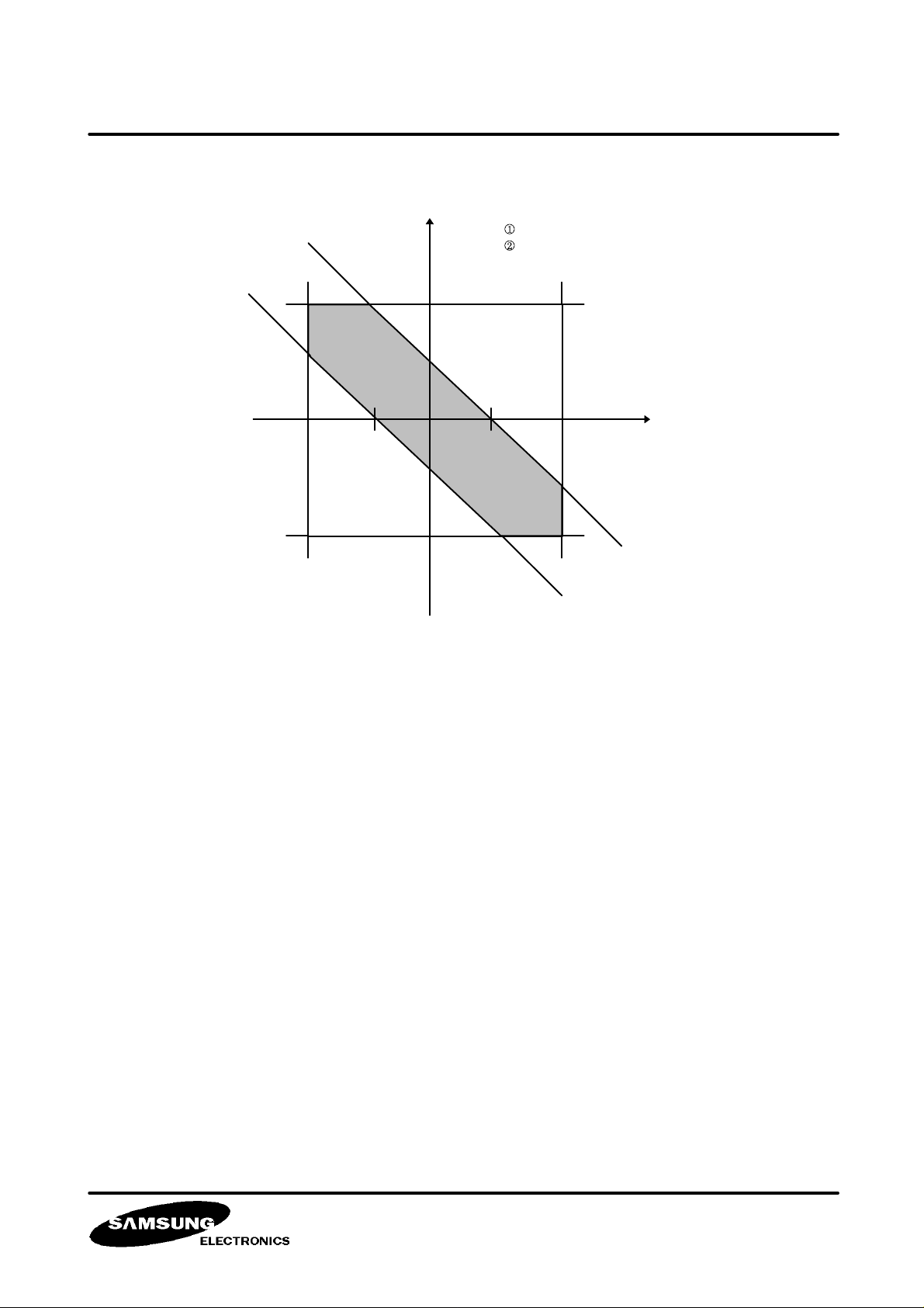
-ORBYTH
R-Y
R-Y, B-Y Coordinate for AWB
OYL_AWB < Y < OYH_AWB
ORYTH
ORBYTH
-OBYTH
-ORYTH
<AWB Active Area in Y, R-Y, B-Y>
OBYTH
73. ADDRESS 5C
1) OW2SH <7:0> : OPT_DETECT Horizontal Start point Window2 for AF
- DATA <7:0>
- RANGE : 3 ≤ OW2SH ≤ 251
74. ADDRESS 5D
1) OW2EH <7:0> : OPT_DETECT Horizontal End point Window2 for AF
- DATA <7:0>
- RANGE : 3 ≤ OW2EH ≤ 255
B-Y
75. ADDRESS 5E
1) OW2SV <7:0> : OPT_DETECT Vertical Start point Window2 for AF
- DATA <7:0>
- RANGE : 2 ≤ OW2SH ≤ 121
76. ADDRESS 5E
1) OW2EV <7:0> : OPT_DETECT Vertical End point Window2 for AF
- DATA <7:0>
- RANGE : 3 ≤ OW2SH ≤ 122
VID-97-D004
February 1997
40
Page 41

KS7306 DIGITAL CAMERA PROCESSOR
77. ADDRESS 60
1) OAWO <23:16> : (OA1W1H<7:0>) : OPT_DETECT AF1 accumulation result of Window1
- DATA <7:0>
78. ADDRESS 61
1) OAWO <7:0> : (OA2W1L<7:0>) : OPT_DETECT AF2 accumulation result of Window1
- DATA <7:0>
79. ADDRESS 62
1) OAWO <15:8> : (OA2W1M<7:0>) : OPT_DETECT AF2 accumulation result of Window1
- DATA <7:0>
80. ADDRESS 63
1) OAWO <23:16> : (OA2W1H<7:0>) : OPT_DETECT AF2 accumulation result of Window1
- DATA <7:0>
81. ADDRESS 64
1) OAWO <7:0> : (OA1W2L<7:0>) : OPT_DETECT AF1 accumulation result of Window2
- DATA <7:0>
82. ADDRESS 65
1) OAWO <15:8> : (OA1W2M<7:0>) : OPT_DETECT AF1 accumulation result of Window2
- DATA <7:0>
83. ADDRESS 66
1) OAWO <23:16> : (OA1W2H<7:0>) : OPT_DETECT AF1 accumulation result of Window2
- DATA <7:0>
84. ADDRESS 68
1) OADR <5:0> : OPT_DETECT loadable RAM Address
- DATA <5:0>
- RANGE : 0 ~ 63
85. ADDRESS 69
1) OMDO <7:0> (OMDL<7:0>) : OPT_DETECT RAM Data
- DATA <7:0>
86. ADDRESS 6A
1) OMDO <15:8> (OMDH<7:0>) : OPT_DETECT RAM Data
- DATA <7:0>
VID-97-D004
February 1997
41
Page 42

KS7306 DIGITAL CAMERA PROCESSOR
87. ADDRESS 6B
1) OACCO <7:0> (OACCL<7:0>) : OPT_DETECT AE/AWB Accumulation result
- DATA <7:0>
88. ADDRESS 6C
1) OACCO <15:8> (OACCM<7:0>) : OPT_DETECT AE/AWB Accumulation result
- DATA <7:0>
89. ADDRESS 6D
1) OACCO <23:16> (OACCH<7:0>) : OPT_DETECT AE/AWB Accumulation result
- DATA <7:0>
90. ADDRESS 6E
1) OAWO <7:0> (OA1W1L<7:0>) : OPT_DETECT AF1 Accumulation result of Window1
- DATA <7:0>
91. ADDRESS 6F
1) OAWO <15:8> (OA1W1M<7:0>) : OPT_DETECT AF1 Accumulation result of Window1
- DATA <7:0>
92. ADDRESS 70
1) OWV <5:0> : OPT_DETECT Vertical Subwindow Width of AE/AWB Window
- DATA <5:0>
- RANGE : 3 ≤ OWV ≤ 40
93. ADDRESS 71
1) OWH <4:0> : OPT_DETECT Horizontal Subwindow Width of AE/AWB Window
- DATA <4:0>
- RANGE : 3 ≤ OWH ≤ 31
- Real Point
94. ADDRESS 77
1) OAWO <7:0> (OA2W2L<7:0>) : OPT_DETECT AF2 Accumulation result of Window2
- DATA <7:0>
95. ADDRESS 78
1) OAWO <15:8> (OA2W2M<7:0>) : OPT_DETECT AF2 Accumulation result of Window2
- DATA <7:0>
96. ADDRESS 79
1) OAWO <23:16> (OA2W2H<7:0>) : OPT_DETECT AF2 Accumulation result of Window2
- DATA <7:0>
VID-97-D004
February 1997
42
Page 43

KS7306 DIGITAL CAMERA PROCESSOR
97. ADDRESS 7A
1) OAP1W1 <7:0> : OPT_DETECT Peak hold result for AF1 of Window1
- DATA <7:0>
98. ADDRESS 7B
1) OAP2W1 <7:0> : OPT_DETECT Peak hold result for AF2 of Window1
- DATA <7:0>
99. ADDRESS 7C
1) OAP1W2 <7:0> : OPT_DETECT Peak hold result for AF1 of Window2
- DATA <7:0>
100. ADDRESS 7D
1) OAP2W2 <7:0> : OPT_DETECT Peak hold result for AF2 of Window2
- DATA <7:0>
101. ADDRESS 7E
1) OWSV <7:0> : OPT_DETECT Vertical Subwindow Start point of AE/AWB Window
- DATA <7:0>
- RANGE : 21 ≤ OWSV ≤ 228
102. ADDRESS 7F
1) OWSH <7:0> : OPT_DETECT Horizontal Subwindow Start point of AE/AWB Window
- DATA <7:0>
- RANGE : 3 ≤ OWSVH ≤ 231
103. ADDRESS 80
1) POBSEL : PREPROCESS Optical Black Selection
- DATA <4>
- POBSEL = ″0″ :Select CCD Optical Black data
POBSEL = ″1″ : Select MICOM data
2) PDEFECT1 : PREPROCESS DEFECT enable signal
- DATA <3>
- PDEFECT = ″0″ : Select Defect disable
PDEFECT = ″1″ : Select Defect enable
3) PDEFECT2 : PREPROCESS DEFECT enable signal
- DATA <2>
- PDEFECT = ″0″ : Select Defect disable
PDEFECT = ″1″ : Select Defect enable
4) PCORRECT : PREPROCESS defect Correction enable signal
- DATA <1>
PCORRECT = ″0″ : Select Defect Correction disable
PCORRECT = ″1″ : Select Defect Correction enable
5) PDCLAMP : PREPROCESS Digital CLAMP enable signal
- DATA <0>
PDCLAMP = ″0″ : Select Digital Clamp disable
PDCLAMP = ″1″ : Select Digital Clamp enable
VID-97-D004
February 1997
43
Page 44

KS7306 DIGITAL CAMERA PROCESSOR
104. ADDRESS 81
1) PDEFECT_TH <7:0> : PREPROCESS DEFECT THreshold value
- DATA <7:0>
105. ADDRESS 82
1) PHCNT_REF <9:8> : PREPROCESS Horizontal CouNT REFerence value
- DATA <1:0>
106. ADDRESS 83
1) PHCNT_REF <7:0> : PREPROCESS Horizontal CouNT REFerence value
- DATA <7:0>
107. ADDRESS 84
1) PVCNT_REF <7:0> : PREPROCESS Vertical CouNT REFerence value
- DATA <7:0>
108. ADDRESS 85
1) PHSTART <3:0> : PREPROCESS Defect Correction Horizontal START point
- DATA <7:4>
2) PVSTART <3:0> : PREPROCESS Defect Correction Veritical START point
- DATA <3:0>
109. ADDRESS 86
1) PCLP_START <7:0> : PREPROCESS Digital Clamp optical black start point
- DATA <7:0>
110. ADDRESS 87
1) POB_MICOM <9:8> : PREPROCESS Digital Clamp optical black data from MICOM
- DATA <1:0>
111. ADDRESS 88
1) POB_MICOM <7:0> : PREPROCESS Digital Clamp optical black data from MICOM
- DATA <7:0>
112. ADDRESS 89
1) PSG_ POS1 <3:0> : PREPROCESS SG pulse ODD field POSition
- DATA <7:4>
2) PSG_ POS2 <3:0> : PREPROCESS SG pulse EVEN field POSition
- DATA <3:0>
VID-97-D004
February 1997
44
Page 45

KS7306 DIGITAL CAMERA PROCESSOR
113. ADDRESS 90
1) PA1 <7:0> : PREPROCESS Defect Vertical & Horizontal Address 1 of first field
- DATA <7:0>
114. ADDRESS 91
1) PA1 <15:8> : PREPROCESS Defect Vertical & Horizontal Address 1 of first field
- DATA <7:0>
115. ADDRESS 92
1) PA1 <18:16> : PREPROCESS Defect Vertical & Horizontal Address 1 of first field
- DATA <2:0>
2) PA1 <2:0> : PREPROCESS Defect Vertical & Horizontal Address 1 of second field
- DATA <6:4>
116. ADDRESS 93
1) PA2 <7:0> : PREPROCESS Defect Vertical & Horizontal Address 2 of first field
- DATA <7:0>
117. ADDRESS 94
1) PA2 <15:8> : PREPROCESS Defect Vertical & Horizontal Address 2 of first field
- DATA <7:0>
118. ADDRESS 95
1) PA2 <18:16> : PREPROCESS Defect Vertical & Horizontal Address 2 of first field
- DATA <2:0>
1) PA2 <2:0> : PREPROCESS Defect Vertical & Horizontal Address 2 of second field
- DATA <6:4>
119. ADDRESS 96
1) PA3 <7:0> : PREPROCESS Defect Vertical & Horizontal Address 3 of first field
- DATA <7:0>
120. ADDRESS 97
1) PA3 <15:8> : PREPROCESS Defect Vertical & Horizontal Address 3 of first field
- DATA <7:0>
121. ADDRESS 98
1) PA3 <18:16> : PREPROCESS Defect Vertical & Horizontal Address 3 of first field
- DATA <2:0>
2) PB3 <2:0> : PREPROCESS Defect Vertical & Horizontal Address 3 of second field
- DATA <6:4>
VID-97-D004
February 1997
45
Page 46
KS7306 DIGITAL CAMERA PROCESSOR
122. ADDRESS 99
1) PA4 <7:0> : PREPROCESS Defect Vertical & Horizontal Address 4 of first field
- DATA <7:0>
123. ADDRESS 9A
1) PA4 <15:8> : PREPROCESS Defect Vertical & Horizontal Address 4 of first field
- DATA <7:0>
124. ADDRESS 9B
1) PA4 <18:16> : PREPROCESS Defect Vertical & Horizontal Address 4 of first field
- DATA <2:0>
2) PB4 <2:0> : PREPROCESS Defect Vertical & Horizontal Address 4 of second field
- DATA <6:4>
125. ADDRESS A0
1) ENP : Encoding Nega/Posi effect
- DATA <7>
ENP OPERATION
0 Normal Operation (POSI)
1
2) EART <2:0> : Encoder ARTfereeze effect
- DATA <6:4>
EART <2><1><0> OPERATION
0 0 0 256 Level
0 0 1 128 Level
0 1 0 64 Level
0 1 1 32 Level
1 0 0 16 Level
1 0 1 8 Level
Level Conversion (NEGA)
⇒ Refered White Clip Level
1 1 0 4 Level
1 1 1 2 Level
VID-97-D004
February 1997
46
Page 47
KS7306 DIGITAL CAMERA PROCESSOR
3) EYDL <3:0> : Encoder Y signal Delay control selection
- DATA <3:0>
EART <3><2><1><0> DELAY
0 0 0 0 0 Delays
0 0 0 1 +1 Delays
0 0 1 0 +2 Delays
0 0 1 1 +3 Delays
0 1 0 0 +4 Delays
0 1 0 1 +5 Delays
0 1 1 0 +6 Delays
0 1 1 1 +7 Delays
126. ADDRESS A1
1) EYGAIN <7:0> : Encoder Y signal GAIN
- DATA <7:0>
- RANGE : 0X ~ 1X
- FORMAT : 0.XXXXXXXX
127. ADDRESS A2
1) ECGAIN <7:0> : Encoder Color signal GAIN
- DATA <7:0>
- RANGE : 0X ~ 1X
- FORMAT : 0.XXXXXXXX
EART <3><2><1><0> DELAY
1 0 0 0 -5 Delays
1 0 0 1 -5 Delays
1 0 1 0 -5 Delays
1 0 1 1 -5 Delays
1 1 0 0 -4 Delays
1 1 0 1 -3 Delays
1 1 1 0 -2 Delays
1 1 1 1 -1 Delays
128. ADDRESS A3
1) EDZCBLKOFF: Encoder digital zoom mode CBLK OFF
- DATA <7>
EDZCBLKOFF = ″0″
EDZCBLKOFF = ″1″
2) ECIFI : Encoder EC_IF block input selection for test
- DATA <6>
3) ECIFI : Encoder EC_IF block input selection for test
- DATA <5>
4) ESU <4:0>: Encoder lumanance signal Set-up level
- DATA <4:0>
ON
OFF
129. ADDRESS A4
1) EWC <7:0> : Encoder White Clip Control
- DATA <7:0>
VID-97-D004
February 1997
47
Page 48
KS7306 DIGITAL CAMERA PROCESSOR
130. ADDRESS A5
1) EBLK <7:0> : Encoder lumanance signal BLanK level
- DATA <7:0>
131. ADDRESS A6
1) EUSC <7:0> : Encoder U(B-Y) Signal burst level Control
- DATA <7:0>
132. ADDRESS A7
1) EVSC <7:0> : Encoder V(R-Y) Signal burst level Control
- DATA <7:0>
- RANGE : 0 ~ 80 RE
BURST
R-Y
<NTSC System>
BURST
B-Y
<PAL System>
R-Y
Line n,(LALT=0)
133. ADDRESS A8
1) EBMCK_SEL: Encoder balanced modulation clock selection
- DATA <7>
EBMCK_SEL = ″0″
EBMCK_SEL = ″1″
Select FSC clock
Select 4FSC clock
B-Y
R-Y
B-Y
BURST
<PAL System>
Line n+1,(LALT=1)
VID-97-D004
February 1997
48
Page 49

KS7306 DIGITAL CAMERA PROCESSOR
2) EDLY_SEL <3:0> : Encoder Delay Selection
- DATA <5:2>
EDLY_SEL <3><2><1><0> DELAY
X X 0 0 0 Delays for CSYNCO
X X 0 1 1 Delays for CSYNCO
X X 1 0 2 Delays for CSYNCO
X X 1 1 3 Delays for CSYNCO
0 0 X X 0 Delays for BFO
0 1 X X 1 Delays for BFO
1 0 X X 2 Delays for BFO
1 1 X X 3 Delays for BFO
3) EBFDLY <1:0> : Encoder BF signal DeLaY Selection
- DATA <2:0>
EBFDLY <2><1><0> Delay EBFDLY <2><1><0> Delay
0 0 0 0 Delays 1 0 0 4 Delays
0 0 1 1 Delays 1 0 1 5 Delays
0 1 0 2 Delays 1 1 0 6 Delays
0 1 1 3 Delays 1 1 1 7 Delays
134. ADDRESS A9
1) EFSC_CONT: Encoder FSC clock control
- DATA <2>
EFSC_CONT = ″0″
EFSC_CONT = ″1″
2) EFSC2_CONT: Encoder FSC2 clock control
- DATA <1>
EFSC2_CONT = ″0″
EFSC2_CONT = ″1″
Pass the FSC clock
Invert the FSC clock
Pass the FSC2 clock
Invert the FSC2 clock
VID-97-D004
February 1997
49
Page 50
KS7306 DIGITAL CAMERA PROCESSOR
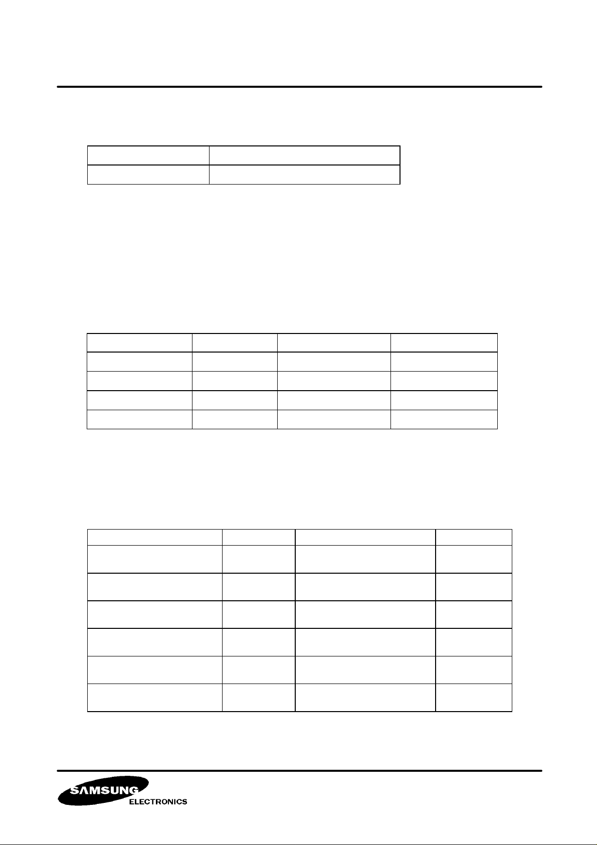
3) EFSC_RN_SEL: Encoder FSC reset selection
- DATA <0>
EFSC_RN_SEL = ″0″
EFSC_RN_SEL = ″1″
138. ADDRESS E0
135. ADDRESS E0
System reset & Reset pulse each 4 HD
Only system reset
1) CBHN <7:0> : Color difference signal (B-Y) Hue Control Negative Gain
- DATA <7:0>
- RANGE : 00H ~ 7FH (-1X ~ 1X), 2 ′S complement
139. ADDRESS E0
136. ADDRESS FA
1) S1 <7:0> : Delay Control Selection
- DATA <3:0>
S<3> <2><1><0> Delay S<3> <2><1><0> Delay
× × 0 0
× × 0 1
× × 1 0
× × 1 1
4 Delays for HD
5 Delays for HD
6 Delays for HD
7 Delays for HD
0 0 × ×
0 1 × ×
1 0 × ×
1 1 × ×
4 Delays for PBLK
3 Delays for PBLK
2 Delays for PBLK
1 Delays for PBLK
137. ADDRESS FA
137. ADDRESS FB
1) S2 <7:0> : Delay Control Selection
- DATA <5:0>
S <5><4><3><2><1><0> MODE S <5><4><3><2><1><0> MODE
X X X X 0 0
X X X X 0 1
X X X X 1 0
X X X X 1 1
X X 0 0 X X
X X 0 1 X X
36 Delays for
CBLK
37 Delays for
CBLK
38 Delays for
CBLK
39 Delays for
CBLK
36 Delays for
CSYNK
37 Delays for
CSYNK
X X 1 0 X X
X X 1 1 X X
0 0 X X X X
0 1 X X X X
1 0 X X X X
1 1 X X X X
38 Delays for
CSYNK
39 Delays for
CSYNK
36 Delays for
BF
37 Delays for
BF
38 Delays for
BF
39 Delays for
BF
* KS7314 have to Delay Control variably with considering Delay of ENCODER and DAC.
VID-97-D004
February 1997
50
Page 51
KS7306 DIGITAL CAMERA PROCESSOR
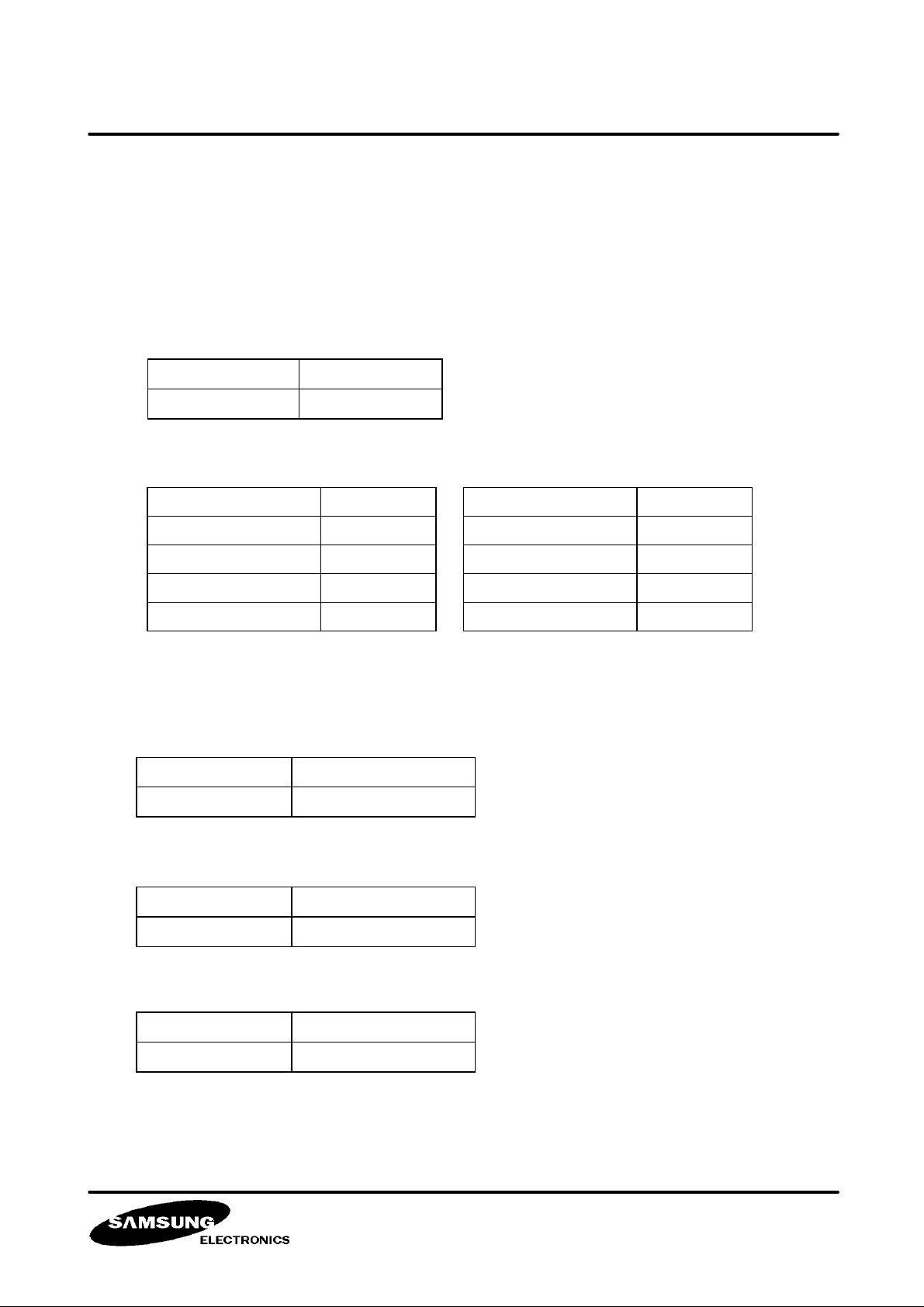
138. ADDRESS FC
1) TSTCMD <7:0> : Test Command
- DATA <7:0>
139. ADDRESS FD
1) FCM : FCM mode
- DATA <7>
FCM = ″0″
FCM = ″1″
2) HSYNCS <2:0> : HSYNC delay Selection
- DATA <5:3>
HSYNCS <2><1><0> DELAY
0 0 0 0 Delays
0 0 1 +1 Delays
0 1 0 +2 Delays
0 1 1 +3 Delays
No FCM mode
FCM mode
140. ADDRESS FE
1) LALT_CONT : LALT signal Control for kasan
- DATA <7>
LALT_CONT = ″0″
LALT_CONT = ″1″
Pass the LALT
Invert the LALT
HSYNCS <2><1><0> DELAY
1 0 0 -4 Delays
1 0 1 -3 Delays
1 1 0 -2 Delays
1 1 1 -1 Delays
2) XCK_CONT : External Clock Control for kasan
- DATA <6>
XCK_CONT = ″0″
XCK_CONT = ″1″
3) MMSEL : MultiMedia Selection
- DATA <4>
MMSEL = ″0″
MMSEL = ″1″
4) HSEL : Horizontal SELection
- DATA <3>
Pass the Clock
Invert the Clock
Normal Operation
Multi-Media Mode
VID-97-D004
February 1997
51
Page 52
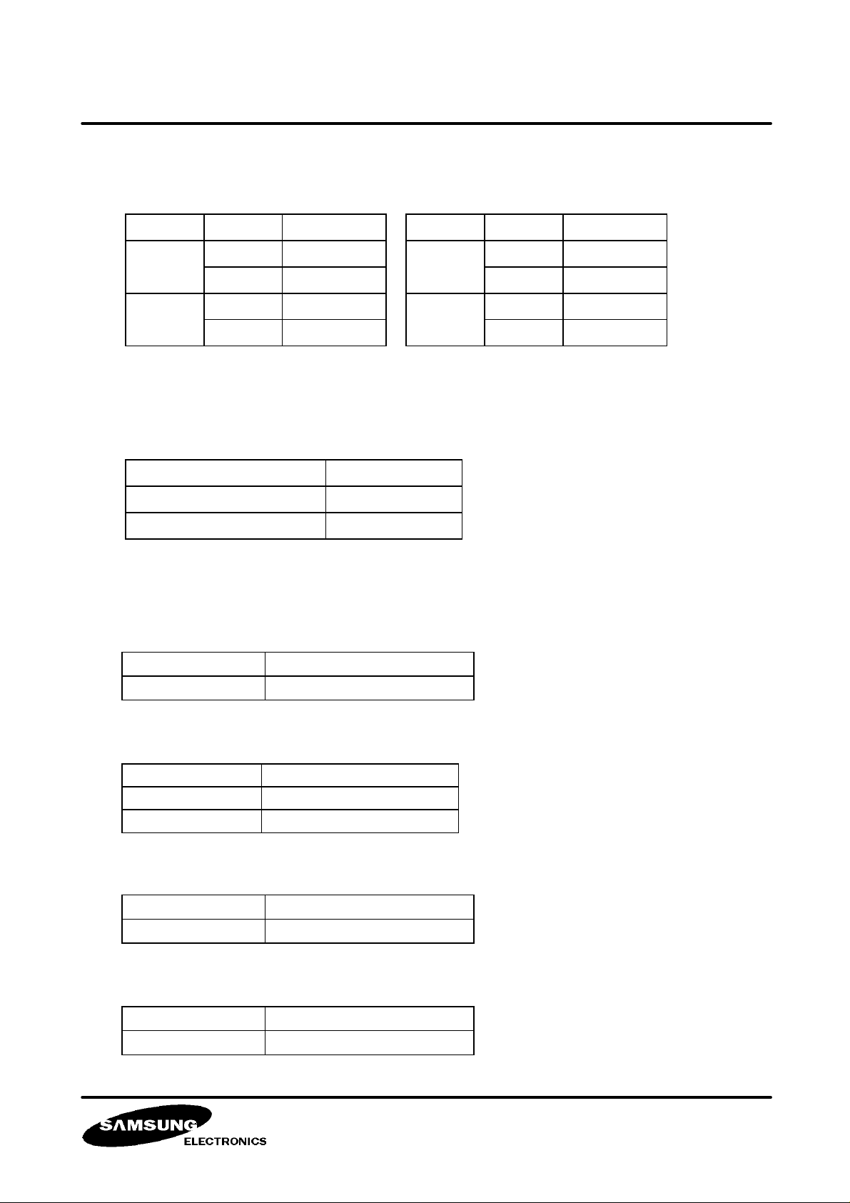
KS7306 DIGITAL CAMERA PROCESSOR
5) VSEL : Vertical SELection
- DATA <2>
HSEL SCK CCD INPUT
0 S2
0
1 S1
0 S1
1
1 S2
6) SCK_CONT : S-ClocK CONTrol
- DATA <1>
7) UVCK_CONT : UV-ClocK CONTrol
- DATA <0>
SCK_CONT, UVCK_CONT OPERATION
0 Pass The Clock
1 Invert The Clock
141. ADDRESS FF
1) SYNCSH : SYNC wave SHape
- DATA <7>
VSEL ID CCD INPUT
0 CR
0
1 CB
0 CB
1
1 CR
SYNCSH = ″0″
SYNCSH = ″1″
2) EXT_DAC : Used External DA Converter
- DATA <6>
EXT_DAC OPERATION
0 Using Internal DAC
1 Using External DAC
3) C422 : 4:2:2 mode for test
- DATA <5>
C422 = ″0″
C422 = ″1″
4) WIDE mode
- DATA <4>
WIDE = ″0″
WIDE = ″1″
Sync wave No Shaping mode
Sync wave Shaping mode
Select 4 Bit Chroma Output
Select 8 Bit Chroma Output
Not WIDE mode
WIDE mode
VID-97-D004
February 1997
52
Page 53
KS7306 DIGITAL CAMERA PROCESSOR
5) OLPFSEL : LPF Selection for OPT_DETECT
- DATA <3>
OLPFSEL = ″0″
OLPFSEL = ″1″
H(Z) = 0.25+0.5Z-1+0.25Z
H(Z) = 0.03125+0.25Z-1+0.25Z-2+0.25Z-3+0.25Z-4+0.03125Z
6) PAL : PAL mode
- DATA <2>
PAL = ″0″
PAL = ″1″
7) HI8 : HIband 8mm mode
- DATA <1>
HI8 = ″0″
HI8 = ″1″
8) DZ : Digital Zoom mode
- DATA <0>
DZ = ″ 0 ″
DZ = ″ 1 ″
-2
-5
NTSC mode
PAL mode
Normal mode
Hiband 8mm mode
Not Digital Zoom mode
Digital Zoom mode
VID-97-D004
February 1997
53
Page 54
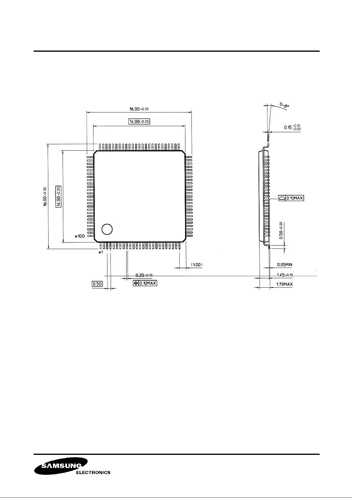
KS7306 DIGITAL CAMERA PROCESSOR
PACKAGE DIMENSION
100 - QFP - 1414 unit: mm
VID-97-D004
February 1997
54
 Loading...