

Page 1
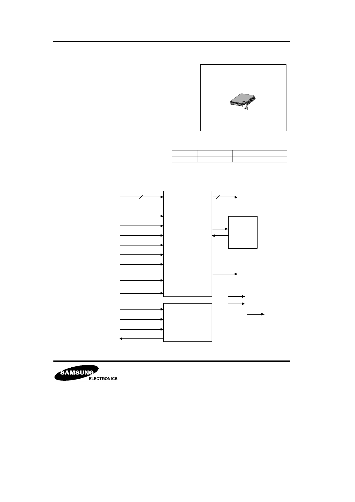
KS7308 FCM
GENERAL DESCRIPTION
FCM(Frequency Conversion Memory) is the high
speed line memory that has two 1024X10bits memory
banks. KS7308 is designed as low power consumption by
CMOS technology. KS7308 is used for camcorder with
digital image stabilizer feature.
FEATURES
- 1024X10bits 2 bank Line memory.
- Independent Read/Write Operation.
- Programmable Read Start Address and
Write Start Address.
- HD Pre-counter for Horizontal blanking.
- Serial-Interface Circuit
- CMOS Double metal technology
- 5V Power supply
BLOCK DIAGRAM
DIO- DI9 (from A/D)
WCK (from TG)
RCK (from TG)
WEN (from TG)
HD (from TG)
VD (from TG)
RSTN(from external)
10
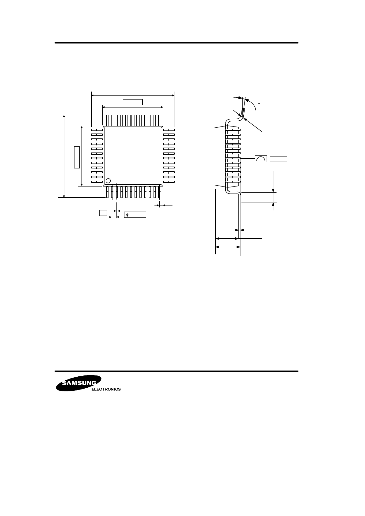
48-QFP-0707
ORDRING INFORMATION
Device Package Operating Temperature
KS7308 48-QFP-0707
10
Momory
Control
0 ~ 70°C
DO0 - DO9
( to DCP )
Momory
Bank
TEST1
TEST2
SCS (from MICOM)
SCK (from MICOM)
SI (from MICOM)
SO (from MICOM)
SIO
( Serial I/O )
HOE
ACTO
NTTO
TOPC
Page 2
KS7308 FCM
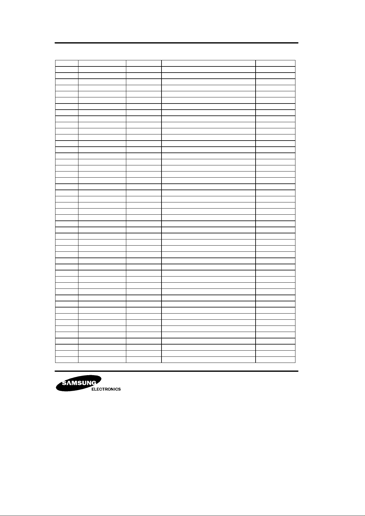
PIN DESCRIPTION
PIN NO. Symbol I/O Description Note
1 VDD1 - Power Supply (5V) vdd5p
2 WCK I Memory write clock from TG
3 RCK I Memory read clock from TG
4 WEN I Memory write enable from TG
5 HD I Horizontal Driving pulse from TG
6 VD I Vertical Driving pulse from TG
7 VDD3 - Power Supply (5V) vdd5i
8 GND3 - Ground vssi
9 RSTN I Reset
10 SCSN I SIO enable from MICOM
11 SCK I SIO clock from MICOM
12 SI I SIO data input from MICOM
13 SO O SIO data output to MICOM
14 DO0 O Data output bit0
15 DO1 O Data output bit1
16 DO2 O Data output bit2
17 DO3 O Data output bit3
18 DO4 O Data output bit4
19 VDD4 - Power Supply (5V) vdd5o
20 GND4 - Ground vsso
21 DO5 O Data output bit5
22 DO6 O Data output bit6
23 DO7 O Data output bit7
24 DO8 O Data output bit8
25 DO9 O Data output bit9
26 HOE O Horizontal odd/even signal output
27 NTTO O Test output (Vin test)
28 ACTO O Test output (Vin test)
29 TOPC I Test input (ACTO control)
30 VDD5 - Power Supply (5V) vdd
31 GND5 - Ground vdd5o
32 TEST0 I Test input (Mode control)
33 TEST1 I Test input (Mode)
34 VDD6 - Power Supply (5V) vdd5p
35 GND6 - Ground vssp
36 DI9 I Data input bit9
37 DI8 I Data input bit8
38 DI7 I Data input bit7
39 DI6 I Data input bit6
40 DI5 I Data input bit5
41 DI4 I Data input bit4
42 VDD1 - Power supply (5V) vdd5i
43 GND1 - Ground vssi
44 DI3 I Data input bit3
45 DI2 I Data input bit2
46 DI1 I Data input bit1
47 DI0 I Data input bit0
48 GND2 - Ground vssp
Page 3
KS7308 FCM
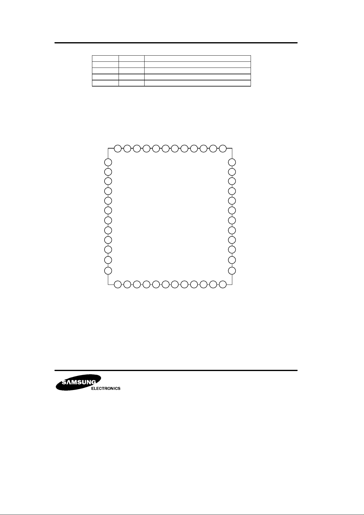
TEST1 TEST0 TEST Mode
0 0 Normal operation
0 1 Memory Function Test
1 0 SRAM-A Read/Write Test
1 1 SRAM-B READ/Write Test
PIN ASSIGNMENT
T
T
E
E
G
D
N
I
D
9
6
36 35 34 33 32 31 30 29 28 27 26 25
S
V
T
D
I
D
G
S
N
T
D
0
5
T
A
O
V
P
D
C
D
N
C
T
H
T
T
O
O
D
O
O
E
9
D 18
D 17
D 16
D 15
D 14
A D D 1
G N D 1
D 13
D 12
D 11
D 10
G N D 2
37
38
39
40
41
W
E
N
KS7308
HDVDV
G
D
D
3
G
N
N
D
D
3
3
42
43
44
45
46
47
48
1 2 3 4 5 6 7 8 9 10 11 12
V
W
D
D
2
R
C
C
K
K
24
D O 8
23
D O 7
22
D O 6
21
D O 5
20
G N D 4
19
V D D 4
18
D O 4
D O 3
17
16
D O 2
15
D O 1
14
D O 0
S O
13
S
S
C
S
N
S
C
I
K
Page 4
KS7308 FCM
*
*
*1, *
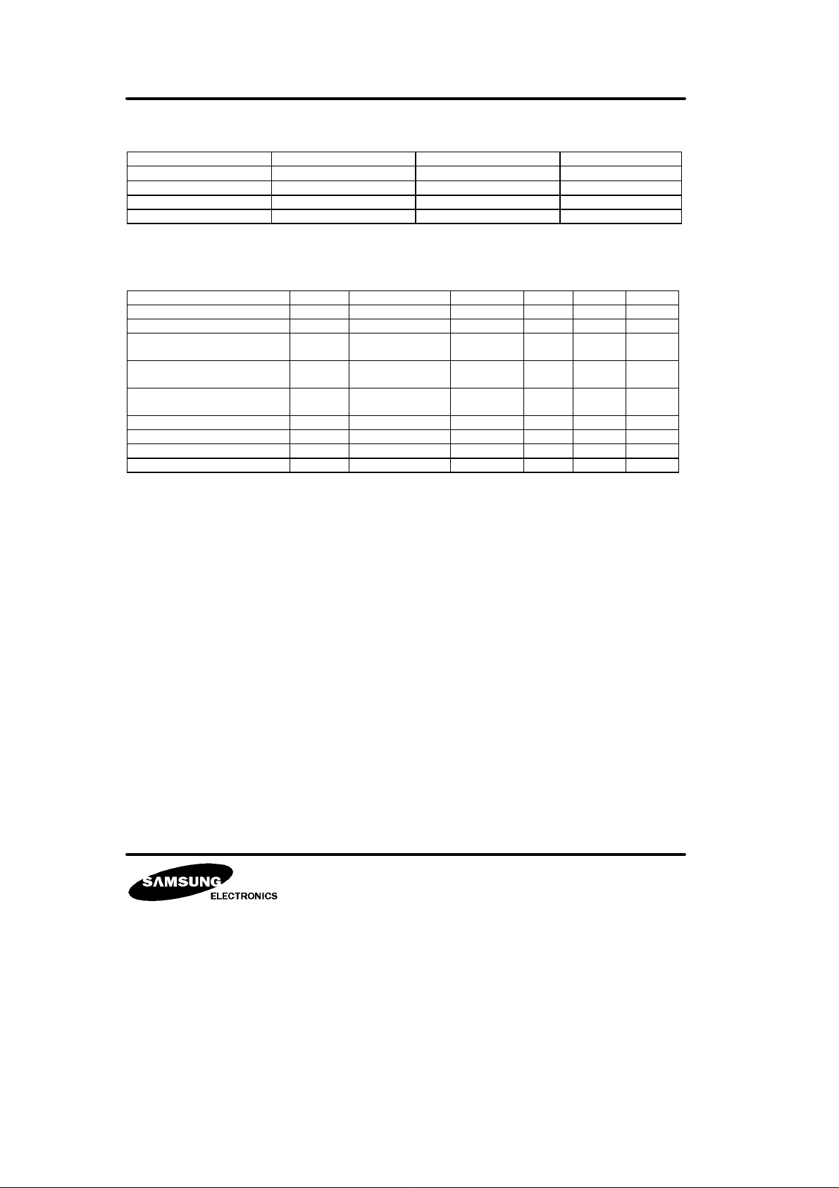
ABSOLUTE MAXIMUM RATINGS
Characteristics Symbol Rating Unit
Storage temperature Tstg -40 ~125
Operating temperature Topr 0 ~ 70
Supply voltage Vdd -0.3 ~ 7.0 V
Input voltage Vin -0.3 ~ Vdd +0.3 V
ELECTRICAL CHARACTERISTICS (Vdd = 4.75 ~ 5.25V Ta = +25°C)
Characteristics Symbol Condition Min Typ Max Unit
Low level input voltage VIL - - 0.3Vdd V
High level input voltage VIH 0.7Vdd - V
Low level output voltage
1
Low level output voltage
2
High level output voltage
2
Input Low current IIL Vin = Vss(Gnd) -10 - +10 uA
Input High current IIH Vin = Vdd -10 - +10 uA
Output leakage current IOZ -10 - +10 uA
Supply current Idd Vin = Vdd - - 40 mA
NOTE : *1 = NTTO,ACTO
*2 = SO, DO [ 9 : 0 ], HOE
VOL1 IOL = 4mA - - 0.4 V
VOL2 IOL = 1mA - - 0.4 V
VOH IOH = 1mA 2.4 - - V
°C
°C
Page 5
KS7308 FCM
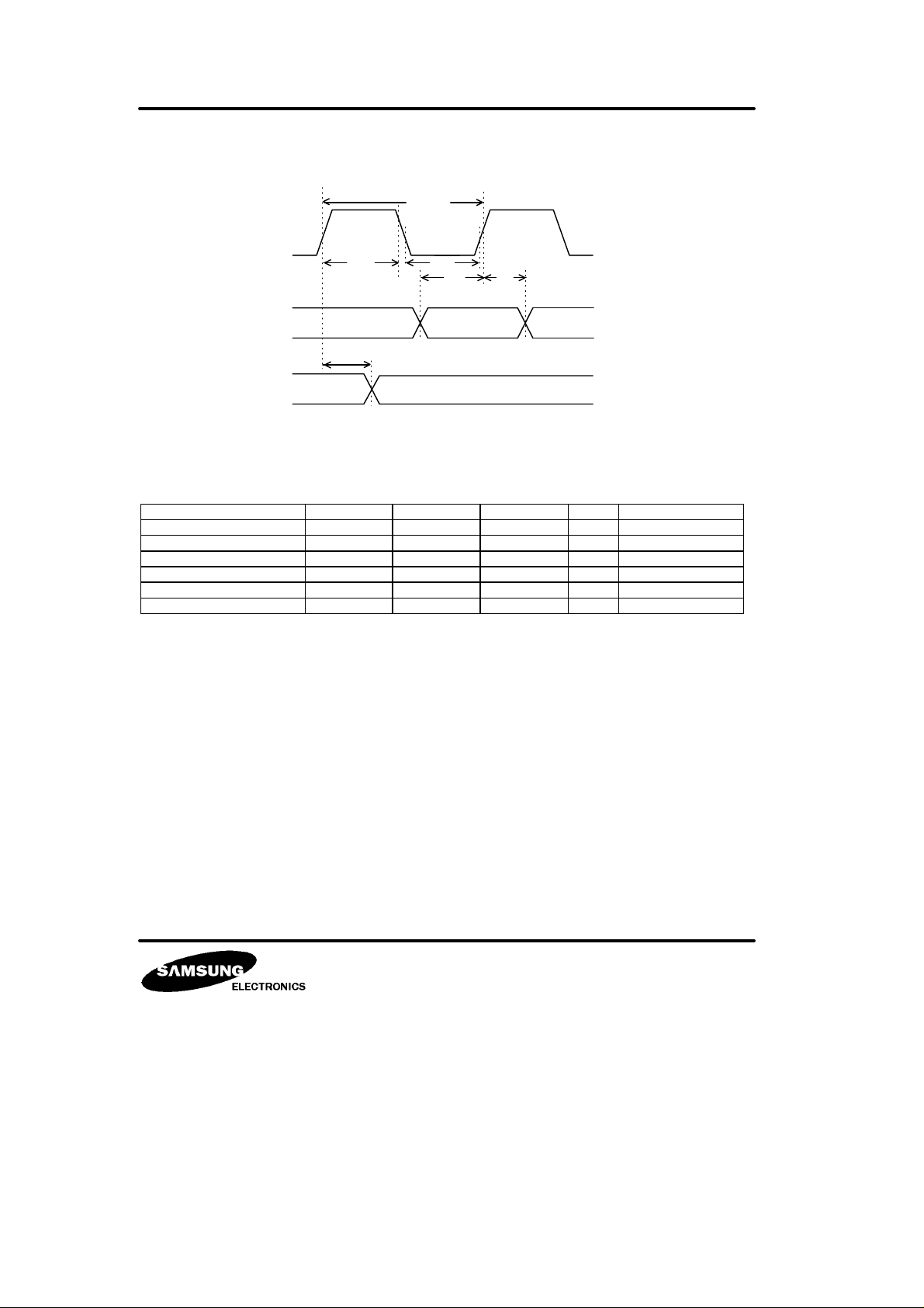
AC ELECTRICAL CHARACTERISTICS
tcpw
WCK
RCK
DI
DO
Vdd = 5.0 V
Characteristics Symbol Min Max Unit
Clock cycle time tcpw 54 tscy ns tscy : SCK clock
Clock high time tchp 20 ns
Clock low time tclp 20 ns
Write data hold time tdh 0 ns
Write data set up time tds 10 ns
Data access time tac 40 ns CL = 75pF
tchp tclp
tds tdh
tac
Page 6
KS7308 FCM
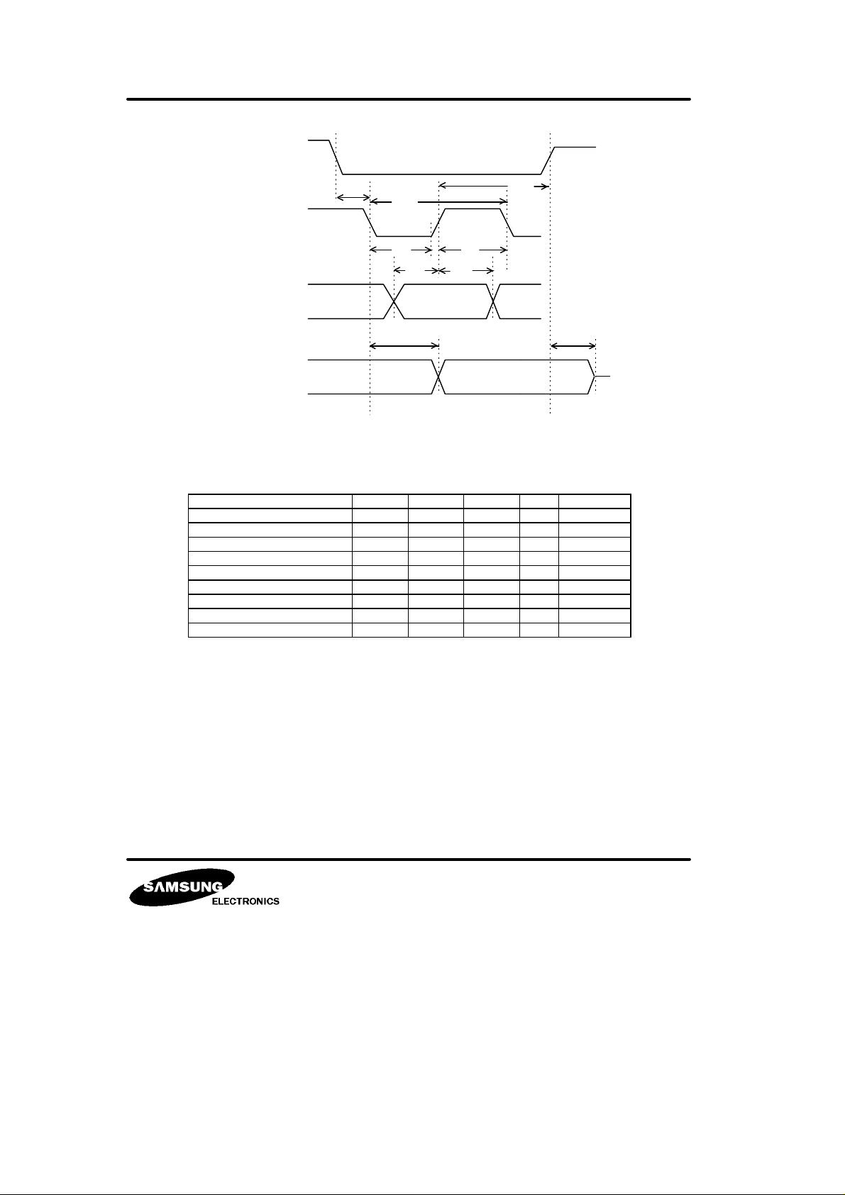
SCSN
tshd
SCK
SI
SO
tscn
tscy
twl twh
tsds tsdh
tsac
Characteristics Symbol Min Max Unit Condition
Serial clock cycle time tscy 2 us
Serial clock high time twh 700 ns
Serial clock low time twl 700 ns
Serial data hold time tsdh 30 ns
Serial data set up time tsds 30 ns
Serial data set access time tsac 500 ns
Serial daa floating time tsdft 20 ns
SCSN set up time tscn 30 ns
SCSN hold time tshd 30 ns
tsdft
Vdd = 5.0
Page 7
KS7308 FCM
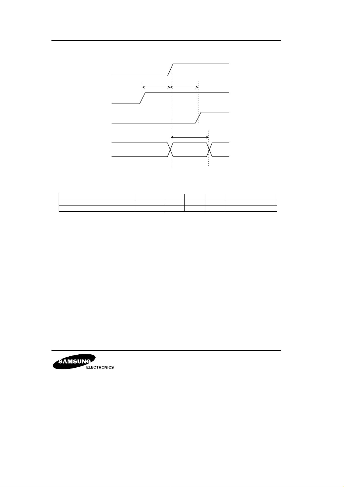
HD
tvdh
VD
VD
WEN
Characteristics Symbol Min Max Unit Condition
VD level hold time tvdh 4 RCK RCL clock
WEN level hold time tweh 5 RCK RCK clock
tvdh
tweh
Vdd = 5.0V
Page 8
KS7308 FCM
OPERATING
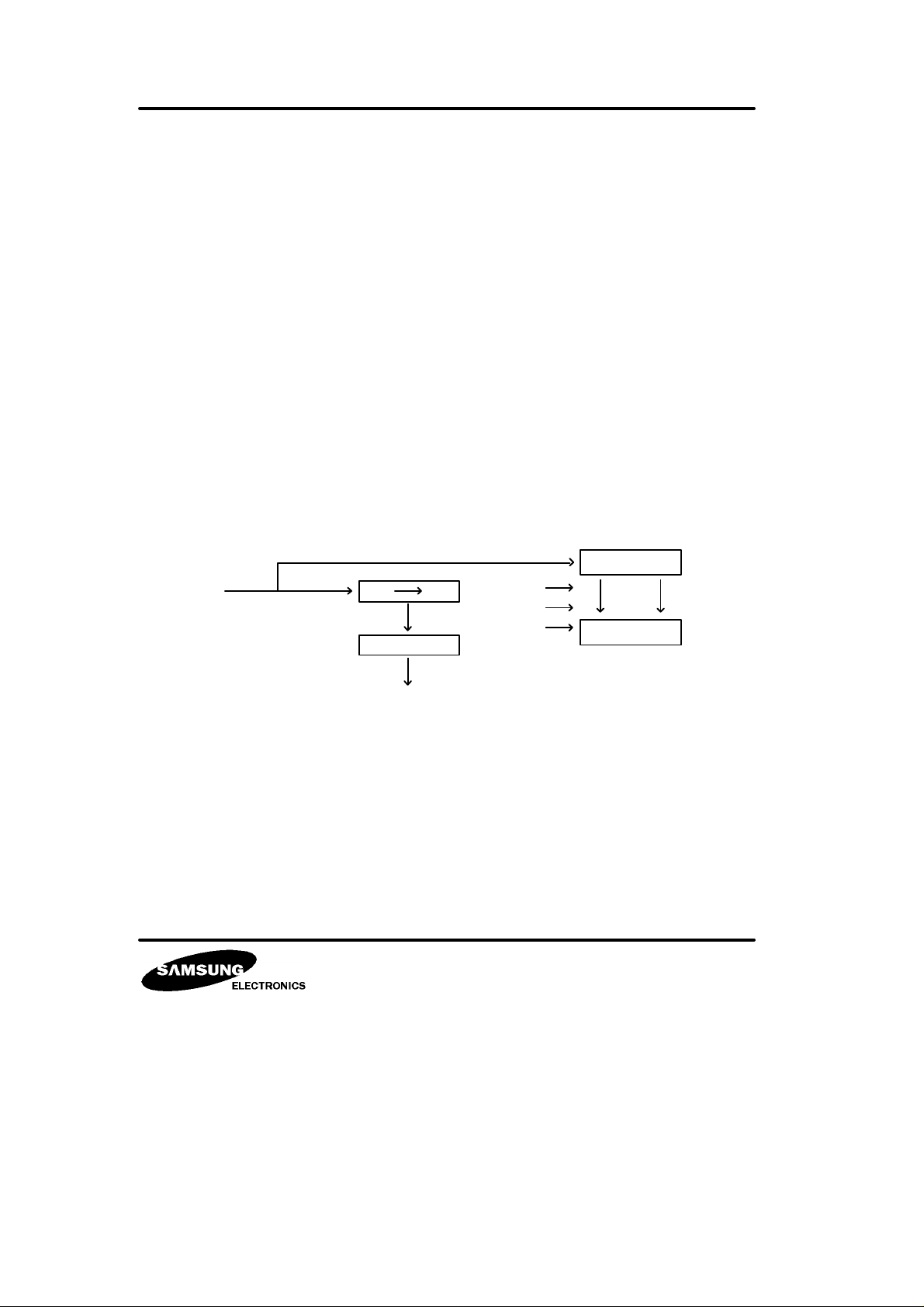
FCM has a SIO which is connected to DIS-MICOM. This SIO type can take 4wire type serial commuication with DISMICOM. MICOM can read the status of serial communication error such as parity error and Stop - Byte error. Read start
address should contain a zoom value and a motion vecter calculated by DIS -MICOM. FCM starts to out data regarding ot
the contents of the read start address resister. Thus, by setting proper read start address, Digital Image Stabilizer can be
realized in a hoizontal direction. FCM has a HD precounter also to eliminate unnecessary data count in the memory bank.
1. DATA ACCESS
FCM supports normal 4 wired serial interface. The serial data is shifted from the MSB side. There are 6 resisters with 8
bit.
These are :
(1) SMOD (Serial Mode Resister)
(2) Read start address reister (2 Byte)
(3) Writer start address resister (2 Byte)
(4) HD precounter resister (1 Byte)
When user want to change one of above register contents, always user has to provide whole contents of each registers.
And STOP Byte should follow. Thus, user has to send total 7 Byte data per each serial communication. For read only
status register is valid for normal operation to check SIO operation condition.
SI
S P
Timing
B u f f e r
W
R
VD
Status
R e g
D e c
R/W fag
Page 9
KS7308 FCM
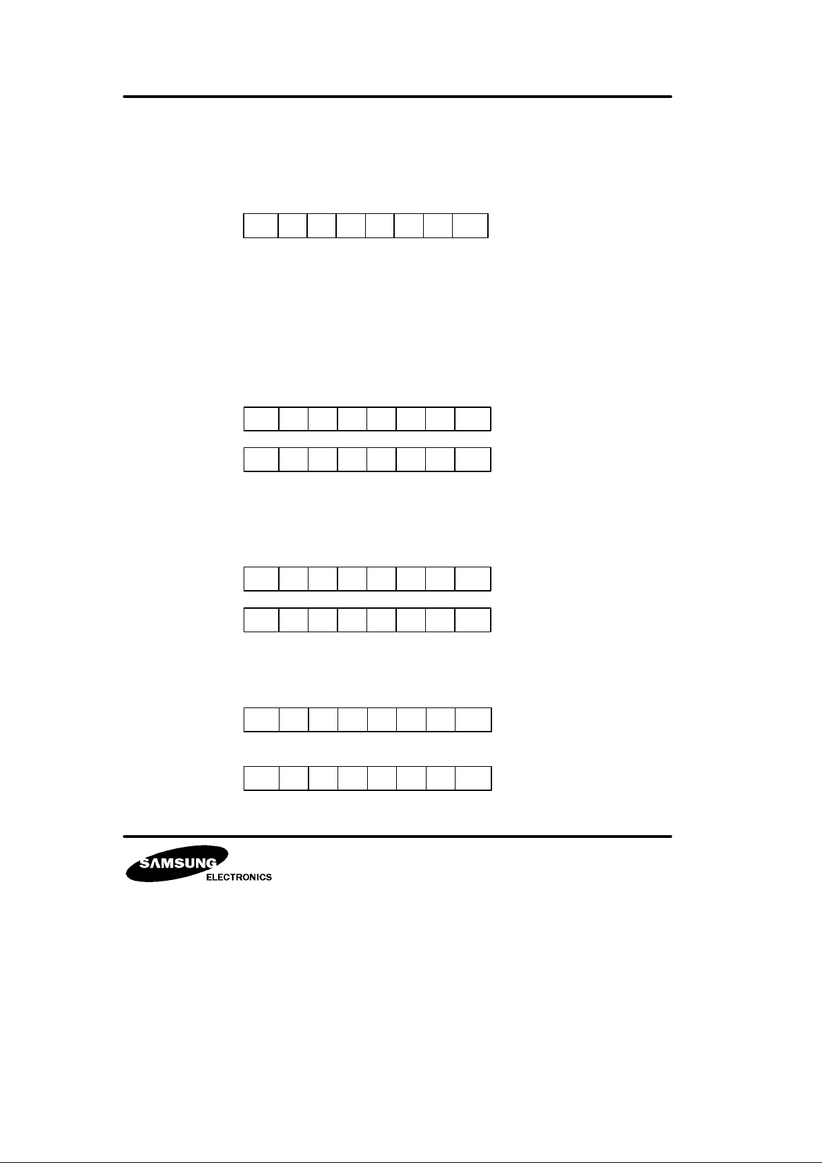
2. SIO REGISTER
[Register diagram]
SMOS resister
MSB
0 0 0 0
(lst Byte)
RE WE
0 0
group address
RE = 0, WE = 1 : Write enable (Write to register)
RE = 1, WE = 0 : Read enable (Read from counter outupt without UD bit)
RE = 0, WE = 0 : No operation RE = 1, WE = 1 : Prohibited
Read start address register (2 Byte)
Defines read start position in the bank memory.
MSB
0 0 0 0
MSB (3rd Byte) LSB
A7 A6 A5 A4
(2nd Byte)
UD
A2
A9 A8
A1 A0
0
A3
UD = 0 : Ciybter increment UD = 1 : Counter decrement
Write start address register (2 Byte)
Defines write start position in the bank memory
MSB
0 0 0 0
MSB (5th Byte) LSB
A7 A6 A5 A4
(4th Byte)
0
A2
A9 A8
A1 A0
0
A3
LSB
LSB
LSB
HD control register
Control to start read address counter incrementation from rising edge of HD.
(6th Byte)
D2
D3
1
0
P : Even parity
LSB
D1 D0
0 P
Stop Byte
MSB
D7 D6 D5 D4
MSB (7th Byte) LSB
1 1 1 0
Page 10
KS7308 FCM
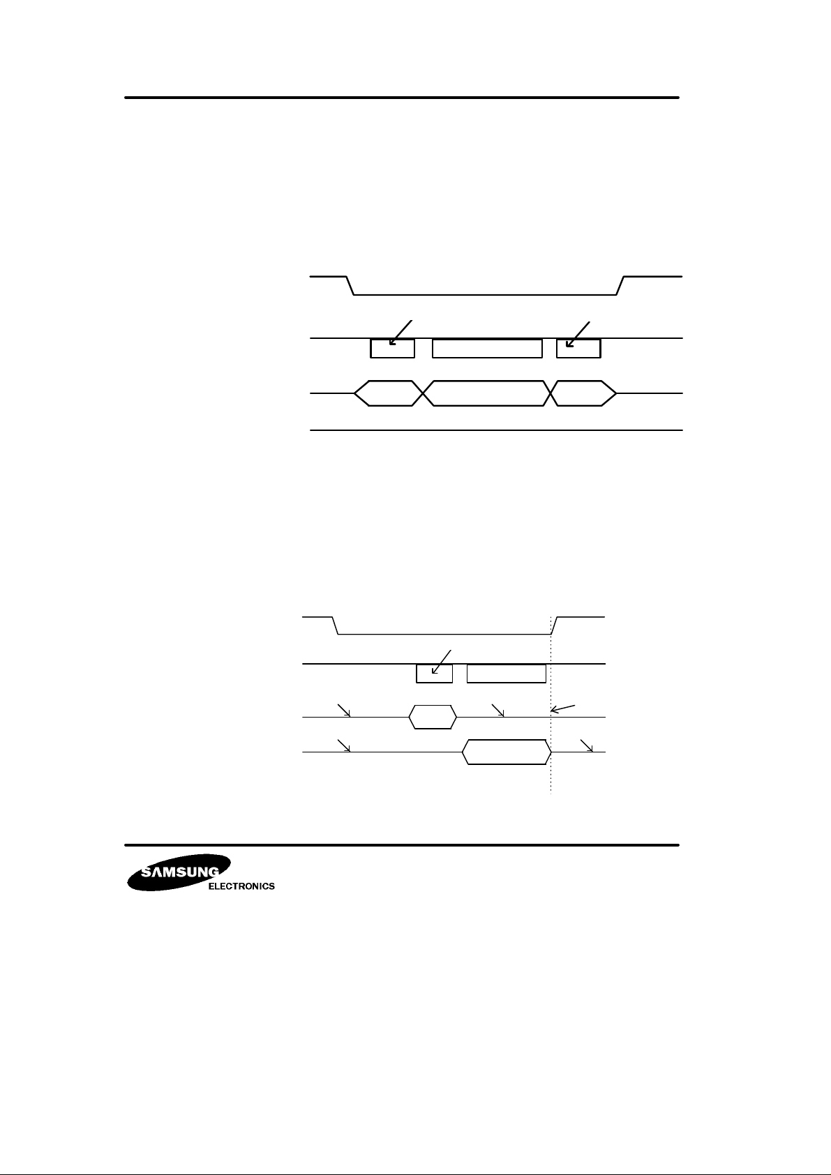
3. MICOM DATA WRITE
(1) First data (SMOD) will entr to S/P buffer from SI for Command decoding. To specify write mode, W - bit has to be set
“1” then. FCM is configurated to accept write access from MICOM.
(2) 4 Address data and HD control data will be written to Serial buffer.
(3) Last data (Stop Byte ) in S/P will be checked such as Stop code and even parity.
(4) Data in serial buffer will be transferd to internal register at VD rising edge.
[Timing diagram ]
SCSN
SCK
SI
SO
0000W
8 clocks 8 clocks
40 clocks
5 Byte data
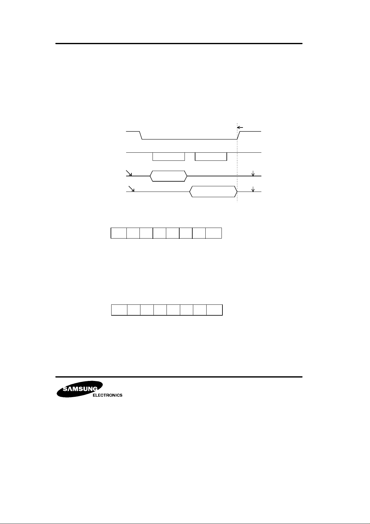
4. MICOM Data Read
(1) First data (SMOD) will enter to S/P buffer from SI for Command decoding.
To specify read mode, R - bit has to be set “1” then. FCM is configured to accept
read operation by driving SO.
(2) 4 counter values (Read Address counter ; 2 Byte, Writer Address counter ; 2 Byte,)
and HD counter value are read out to SO pin.
[Timing diagram ]
SCSN
SCK
Floating area
SI
Floating area Floating area
SO
8 clocks
40 clocks
Floating area
0000R
5Byte data
stop
refer to Electrical spec
Page 11
KS7308 FCM
5. SIO STATUS READ
There is one status register to be read out by MICOM. There are 2 bit flags whigh are PE and WF respectivity.
The MICOM should check this status to test.
(1) Serial communication is successfully completed or not.
(2) Setting data are loaded into each register or not.
It is up to user to judge this flag or not.
[ Timing diagram ]
SCSN
refer to electrical spec
SCK
SI
SO
[ Status register diagram ]
Command
RE = 1, WE = 0 : Read enable
RE = 0, WE = 1 : Prohibited
RE = 0, WE = 0 : Prohibited
RE = 1, WE = 1 : Prohibited
Read data
PE : Register write error flag
PE = 1 : Error
PE = 0 : No Error
Floating area
Floating area
MSB
1 1 1 1
group address
MSB
PE WF 0 0
1111R
( lst Byte )
( 2nd Byte )
RE WE
0 0
8 clocks8 clocks
Floating area
Floating area
status
LSB
0 0
LSB
0 0
WF : Register write status flag
WF = 1 : Waiting for loading into the register
WF = 0 : Loaded
Page 12
KS7308 FCM
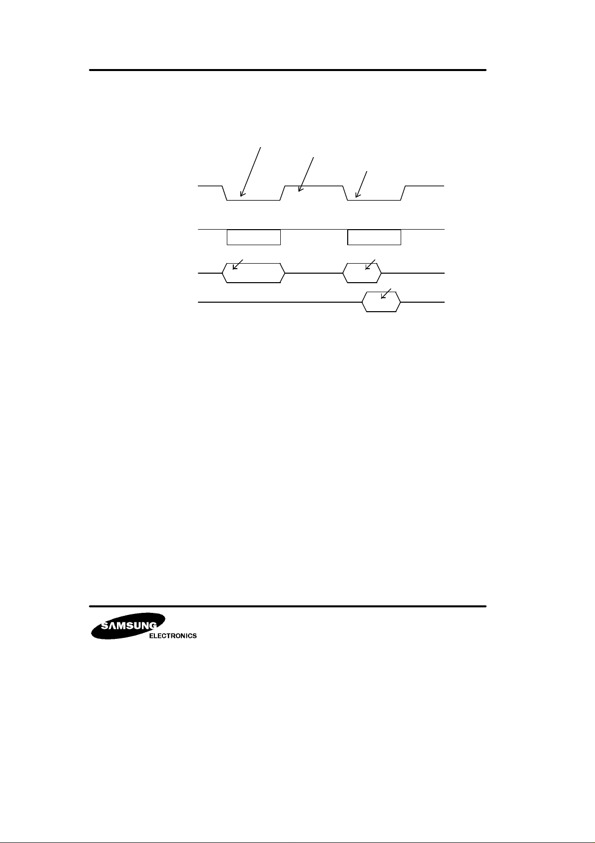
6. SIO COMMUNICATION PROTOCOL
(1) Standard protocol of data write
Data write access
SCSN should turn High
Status read
SCSN
SCK
SMOS / Write data / stop
SI
SO
(2) Invalid write data
When user initiate SIO operation before previouse write operation data is loaded into resister at VD timiing, then
initial data will be broken.
16 clocks56 clocks
SMOD
Status
7. RESET CONDITION
The system should supply reset condition by RSTN pin as low level. FCM will
initialize each register value as follows.
(1) Read/Write address register and Counter is set to “0”
(2) HD register is set to “0”.
(3) SMOD register is set to “0”
(4) SO becomes high impedance state.
Page 13
KS7308 FCM
PKG DIAGRAM
48-QFP-0707
_
_
9.00 + 0.30
7.00 + 0.20
# 48
0.50
Unit : mm
_
9.00 + 0.30
_
7.00 + 0.20
# 1
_
0.18 + 0.10
0.1 MAX
( 0.75 )
0~8
0.13
+ 0.10
- 0.05
0.00 MIN
_
1.40 + 0.10
1.6 MAX
0.10 MAX
_
0.50 + 0.20
 Loading...