


KS57C21408/C21418/P21408 PRODUCT OVERVIEW
1 PRODUCT OVERVIEW
OVERVIEW
The KS57C21408/C21418/P21408 is a SAM47 core-based 4-bit CMOS single-chip microcontroller. It has a
timer/counter and LCD drivers.
The KS57P21408 is especially suited for use in data bank, telephone and LCD general purpose.
It is built around the SAM47 core CPU and contains ROM, RAM, 39 I/O lines, programmable timer/counter,
buzzer output, enough LCD dot matrix, and segment drive pins.
The KS57C21408/C21418/P21408 can be used for dedicated control functions in a variety of applications, and is
especially designed for multi data bank, telephone and LCD game.
OTP
The KS57C21408/C21418 microcontroller is also available in OTP (One Time Programmable) version,
KS57P21408. KS57P21408 microcontroller has an on-chip 8 K-byte one-time-programable EPROM instead of
masked ROM. The KS57P21408 is comparable to KS57C21408/C21418, both in function and in pin
configuration.
1-1

PRODUCT OVERVIEW KS57C21408/C21418/P21408
FEATURES SUMMARY
Memory
• 8192 × 8 bit program memory
• 5120 × 4 bit data memory in KS57C21408
• 2560 x 4 bit data memory in KS57C21418
• 108 x 5 bit display memory
39 I/O Pins
• Input: 6 pins
• I/O: 17 pins
• Output: maximum 16 pins for 1-bit level output
(sharing with segment driver outputs)
8-Bit Basic Timer
• Four internal timer functions
8-Bit Timer/Counter 0
• Programmable 8-bit timer
• External event counter
• Arbitrary clock frequency output
• External clock signal divider
LCD Display
• 12 characters dot matrix display (5 x 7)
• 12 digit display (8 segments)
• 60 segments and 9 common pins
Power-Down Modes
• Idle mode (only CPU clock stops)
• Stop mode (Main-System clock and CPU clock
stops)
Oscillation Sources
• Crystal, ceramic, or External RC for system clock
• Main-system clock frequency: 0.4 MHz - 6MHz
• Sub-system clock frequency: 32,768kHz
• CPU clock divider circuit (by 4,8, or 64)
Instruction Execution Times
• 0.67, 1.33, 10.7 µs at 6MHz
• 0.95, 1.91, 15.3 µs at 4.19 MHz
• 122 µs at 32.768 kHz
Watch Timer
• Time interval generation: 0,5ms, 3,9ms at
32768Hz
• 4 frequency (2/4/8/16 kHz) outputs to BUZ pin
Interrupts
• Three external vectored interrupts: INT0, INT1,
INTP0
• Two internal vectored interrupts: INTB, INTT0
• Two quasi-interrupts: INTW, INT2
Memory Mapped I/O Structure
Operating Temperature
• -45 °C to 85 °C
Operating Voltage Range
• 1.8 V to 5.5 V
Package Type
• 100-pin QFP Package
1-2

KS57C21408/C21418/P21408 PRODUCT OVERVIEW
BLOCK DIAGRAM
XOUT
XIN
INTT0, INTB, INTW
INT0, INT1, INTP0, INT2
8-Bit
Timer/
Counter 0
RESET
Interrupt
Control
Block
XT
IN
Clock
XT
OUT
Instruction
Register
Input Port 0
Input Port 1
P0.0-P0.3/
K0-K3
P1.0/INT0
P1.1/INT1
COM0-COM8
SEG16-SEG59
SEG0-SEG15
/P8.0-P8.15
Watch Timer
Internal
Interrupts
Program
Counter
I/O Port 2
I/O Port 4
Basic Timer
Instruction Decoder
Program
Status Word
I/O Port 5
Arithmetic
LCD
Driver/
Controller
NOTE:
Data memory:
Display memory: 108 x 5 bits
and
Logic Unit
Data and
Display
Memory
5120 x 4 bits in KS57C21408
2560 x 4 bits in KS57C21418
Stack
Pointer
8 K Byte
Program
Memory
I/O Port 6
I/O Port 7
Output Port 8
Figure 1-1. KS57C21408/C21418/P21408 Specified Block Diagram
P2.0/BUZ
P2.1/CLO
P4.0/TCL0
P4.1/TCLO0
P4.2
P5.0-P5.3
P6.0-P6.3/
KS0-KS3
P7.0-P7.3/
KS4-KS7
P8.0-P8.15/
SEG0-SEG15
1-3

PRODUCT OVERVIEW KS57C21408/C21418/P21408
PIN ASSIGNMENTS
SEG39
SEG40
SEG41
SEG42
SEG43
SEG44
SEG45
SEG46
SEG47
SEG48
SEG49
SEG50
SEG51
SEG52
SEG53
SEG54
SEG55
SEG56
SEG57
SEG58
81
82
83
84
85
86
87
88
89
90
91
92
93
94
95
96
97
98
99
100
P6.0/KS0
P6.1/KS1
P6.2/KS2
P6.3/KS3
P7.0/KS4
P7.1/KS5
P7.2/KS6
P7.3/KS7
P2.0/BUZ
P2.1/CLO
TCL0/P4.0
TCLO0/P4.1
SEG59
COM4
COM5
COM6
COM7
COM8
VDD
V
SS
Xout
Xin
TEST
XTin
XTout
RESET
P5.0
P5.1
P5.2
P5.3
1
2
3
4
5
6
7
8
9
10
11
12
13
14
15
16
17
18
19
20
21
22
23
24
25
26
27
28
29
30
31
KS57C21408/C21418
100-QFP 1420C
39
38
37
36
35
34
33
32
40
41
42
43
44
45
46
47
48
49
50
80
79
78
77
76
75
74
73
72
71
70
69
68
67
66
65
64
63
62
61
60
59
58
57
56
55
54
53
52
51
SEG38
SEG37
SEG36
SEG35
SEG34
SEG33
SEG32
SEG31
SEG30
SEG29
SEG28
SEG27
SEG26
SEG25
SEG24
SEG23
SEG22
SEG21
SEG20
SEG19
SEG18
SEG17
SEG16
SEG15/P8.15
SEG14/P8.14
SEG13/P8.13
SEG12/P8.12
SEG11/P8.11
SEG10/P8.10
SEG9/P8.9
1-4
SEG8/P8.8
SEG7/P8.7
SEG6/P8.6
SEG5/P8.5
SEG4/P8.4
SEG3/P8.3
SEG2/P8.2
SEG1/P8.1
SEG0/P8.0
COM3
COM2
COM1
COM0
INT0/P1.0
INT1/P1.1
P0.0/K0
P0.1/K1
P0.2/K2
P0.3/K3
P4.2
Figure 1-2. KS57C21408/C21418 Pin Assignment Diagram

KS57C21408/C21418/P21408 PRODUCT OVERVIEW
PIN DESCRIPTIONS
Table 1-1. Pin Descriptions
Pin Name Pin
P0.0 - P0.3
Type
I
4-bit input port.
Description Circuit
Type
A-1 35-32
Pin
Number
Share Pin
K0-K3
1 and 4-bit read, and test are possible.
Pull-up registers.
P1.0
P1.1
2-bit Input port.
I
1 and 4-bit read, and test are possible, 2-bit pull-up
A-3 37
36
INT0
INT1
resistors are assignable by software.
P2.0
P2.1
2-bit I/O port. 1 and 4-bit read/write, and test are
I/O
possible.
D 23
24
BUZ
CLO
Each individual pin can be specified as input or
output.
2-bit pull-up resistors are assignable by software.
Pull-up resistors are automatically disabled for
output pins.
P4.0
P4.1
P4.2
P5.0 - P5.3
4-bit I/O port. 1, 4, and 8-bit read/write, and test are
I/O
possible.
4-pin unit can be specified as input or output.
4-bit pull-up resistors are assignable by software.
E
E-1
E-1
E-1
29
30
31
25-28
TCL0
TCLO0
Pull-up resistors are automatically disabled for
output pins.
Individual pins are software configurable as opendrain or push-pull output.
P6.0 - P6.3
4-bit I/O port. 1, 4,and 8-bit read/write, and test are
I/O
D-1 7-10 KS0 - KS3
possible.
Each individual pin can be specified as input or
output.
4-bit pull-up resistors are assignable by software.
Pull-up resistors are automatically disabled for
output pins.
P7.0 - P7.3 4-bit I/O port. 1, 4, and 8-bit read/write, and test are
11-14 KS4 - KS7
possible.
4-pin unit can be specified as input or output.
4-bit pull-up resistors are assignable by software.
Pull-up resistors are automatically disabled for
output pins.
P8.0 - P8.15 O 4-bit controllable output.
(Dual function as segment output pins)
SEG16-SEG59 LCD segment display signal output. H-10 58-100
H-9 42-57 SEG0 -
SEG15
-
,1
SEG0 - SEG15 LCD segment display signal output. H-9 42-57 P8.0 - P8.15
COM0 - COM8 LCD common signal output. H-11 38-41
-
2-6
INT0 - INT1 I External interrupts. The triggering edge for INT0,
37-36 P1.0 -P1.1
and INT1 is selectable
KS0 - KS7 I/O Quasi-interrupt input for falling edge detection. 7-14 P6.0 - P7.3
K0 - K3 I Vector interrupt input
35-32 P0.0 - P0.3
K0 - K3: falling edge detection
1-5
PRODUCT OVERVIEW KS57C21408/C21418/P21408
Table 1-1. Pin Descriptions (Continued)
Pin Name Pin
Type
BUZ I/O 2,4,8 kHz or 16kHz frequency output for buzzer
Description Circuit
Type
- 23 P2.0
Pin
Num.
Share Pin
signal.
CLO Clock output - 24 P2.1
Xin, X
out
- Crystal, ceramic or RC oscillator pins for main
- 18, 17 -
system clock.
XTin, XT
out
- Crystal oscillator pins for sub-system clock. - 20, 21 TCL0 I/O External clock input for Timer/Counter 0 - 29 P4.0
TCLO0 I/O Timer/Counter 0 clock output - 30 P4.1
RESET
V
DD
V
SS
TEST I Test input: it must be connected to V
I Reset input (active low). B 22 -
- Power supply. - 15 -
- Ground. - 16 -
SS
- 19 -
1-6
KS57C21408/C21418/P21408 PRODUCT OVERVIEW
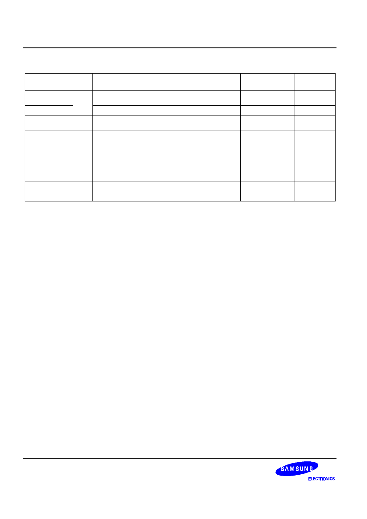
PIN CIRCUIT DIAGRAMS
V
V
DD
Pull-up
Resistor
DD
P-channel
IN
N-channel
Vss
Figure 1-3. Pin Circuit Type A
V
DD
Pull-up
Pull-up
Resistor
Enable
P-channel
IN
Schmitt Trigger
Figure 1-5. Pin Circuit Type A-3
V
DD
Pull-up
Register
Pull-up
Resistor
Enable
IN
Figure 1-4. Pin Circuit Type A-1
P-channel
IN
Schmitt Trigger
Figure 1-6. Pin Circuit Type B
1-7
PRODUCT OVERVIEW KS57C21408/C21418/P21408
V
DD
V
DD
Pull-up
Resistor
Pull-up
Data
P-channel
Resistor
Enable
P-channel
Output
Disable
Pull-Up
Resistor
Enable
Data
Output
Disable
V
SS
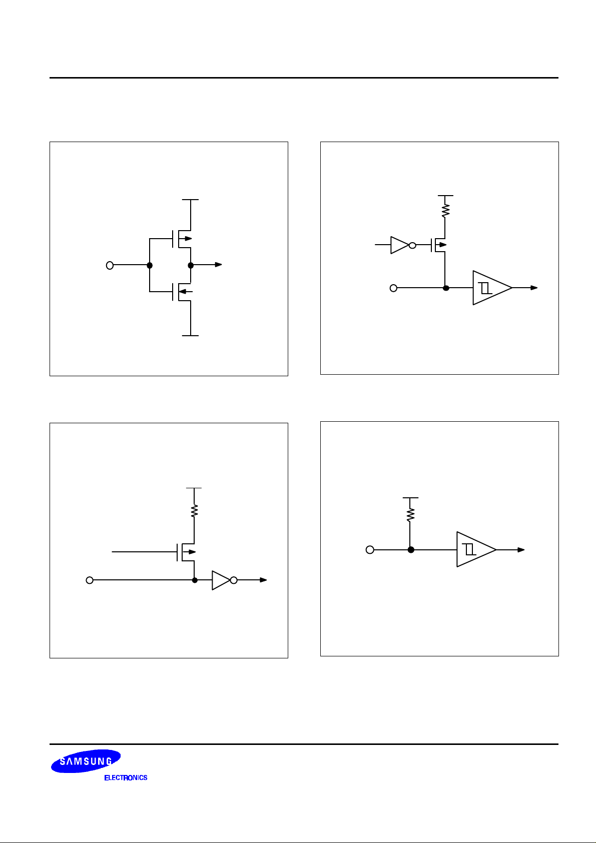
Figure 1-7. Pin Circuit Type C
V
DD
Pull-Up
Resistor
P-channel
Type C
OUT
N-channel
In/Out
Data
Output
Disable
Type C
Schmitt Trigger
Figure 1-9. Pin Circuit Type D-1
VDD
PNE
Data
Output
Disable
VDD
P-channel
N-channel
IN/OUT
Pull-up
Resistor
Pull-up
Resistor
Enable
I/O
1-8
Figure 1-8. Pin Circuit Type D
Schmitt Trigger
Figure 1-10. Pin Circuit Type E
KS57C21408/C21418/P21408 PRODUCT OVERVIEW
V
DD
PNE
V
DD
Pull-up
resistor
Pull-up
V
LC2
Resistor
Data
P-channel
I/O
Enable
Segment
Data
OUT
Output
Disable
Figure 1-11. Pin Circuit Type E-1
SEG Data/P8.0-P8.15
Key
strobe
N-channel
V
V
LC2
LC0
Vss
OUT
V
LC0
Figure 1-13. Pin Circuit Type H-10
V
LC1
COM
Data
Polarity
Vss
V
Vss
DD
OUT
Figure 1-12. Pin Circuit Type H-9
Figure 1-14. Pin Circuit Type H-11
1-9

PRODUCT OVERVIEW KS57C21408/C21418/P21408
NOTES
1-10

KS57C21408/C21418/P21408 ELECTRICAL DATA
13 ELECTRICAL DATA
OVERVIEW
In this section, information on KS57C21408/C21418/P21408 electrical characteristics is presented as tables and
graphics. The information is arranged in the following order:
STANDARD ELECTRICAL CHARACTERISTICS
— Absolute maximum ratings
— D.C electrical characteristics
— Main-system clock oscillator characteristics
— Sub-system clock oscillator characteristics
— I/O capacitance
— A.C electrical characteristics
— Operating voltage range
MISCELLANEOUS TIMING WAVEFORMS
— A.C timing measurement point
— Clock timing measurement at X
— Clock timing measurement at XT
— TCL0 timing
— Input timing for RESET
— Input timing for external interrupts
STOP MODE CHARACTERISTICS AND TIMING WAVEFORMS
— RAM data retention supply voltage in stop mode
— Stop mode release timing when initiated by RESET
— Stop mode release timing when initiated by an interrupt request
in
in
13–1

ELECTRICAL DATA KS57C21408/C21418/P21408
Table 13-1. Absolute Maximum Ratings
(TA = 25 °C)
Parameter Symbol Conditions Rating Units
Supply Voltage
Input Voltage
Output Voltage
High Level
V
V
I
DD
V
O
OH
– – 0.3 to + 6.5 V
Ports 0, 1, 2, 4, 5, 6, 7
I
– 0.3 to V
–
– 0.3 to VDD + 0.3
DD
+ 0.3
One pin – 15 mA
V
V
Output current All output pins – 30 mA
Low Level
Output Current
I
OL
One pin Peak value 30 mA
RMS value
(note)
15 mA
All pins Peak value 100 mA
Operating
RMS value
T
A
– – 40 to + 85
(note)
60 mA
°
C
Temperature
Storage
T
STG
– – 65 to + 150
°
C
Temperature
NOTE : RMS value = Peak Value × Duty .
Table 13-2. D.C Characteristics
(T
= – 40 °C to + 85 °C, VDD = 1.8 V to 5.5 V)
A
Parameter Symbol Conditions Min. Typ. Max. Units
Input High VIH1 Pins except below
Voltage VIH2 Port0, 1, 6, 7, P4.0, RESET
VIH3
XIN, X
OUT
and XT
IN
0.7 V
0.8 V
V
DD
DD
DD
– 0.1
Input Low VIL1 All input pins except below – –
Voltage VIL2 Port0, 1, 6, 7, P4.0, RESET –
Output High
Voltage
VIL3
VOH1
XIN,X
VDD = 4.5 V to 5.5 V
Port2, 4, 5, 6, 7
I
OH
and XT
OUT
= – 1mA
IN
VDD – 1.0
–
–
–
– 0.1
– –
V
DD
V
DD
V
DD
0.3 V
0.2 V
DD
DD
V
13–2

KS57C21408/C21418/P21408 ELECTRICAL DATA
Table 13-2. D.C Characteristics(continued)
(TA = – 40 °C to + 85C, VDD = 1.8 V to 5.5 V)
Parameter Symbol Conditions Min. Typ. Max. Units
Output Low
Voltage
V
OL1
VDD = 4.5 V to 5.5 V
Port2, 4, 5, 6, 7
– – 2
IOL= 15mA
Input High
I
LIH1
Leakage Current
I
LIH2
Input Low
I
LIL1
Leakage Current
I
LIL2
Output High
I
LOH1
Leakage Current
Output Low
I
LOL1
Leakage Current
Pull-up Resistor RL1
RL2
Medium Output
Voltage
(1)
V
V
V
V
OM1
OM2
OM3
OM4
High Output ROH1
VDD = 1.8 V to 5.5 V
– – 0.4
IOL=1.6mA
Vin = V
DD
– – 3
µA
All input pins except below
Vin = V
XIN, X
V
IN
DD
OUT,
= 0 V
XT
IN
All input pins except XIN, X
– – – 3
OUT,
20
XTIN and RESET
V
= 0 V
IN
XIN, X
VO = V
OUT,
DD
XT
IN
– – – 20
– – 3
Port2, 4, 5, 6, 7
VO = 0 V
– – – 3
Port2, 4, 5, 6, 7
V
DD
= 5 V, V
IN
= 0 V
25 50 100
KΩ
All pins except RESET
V
DD
V
DD
RESET
V
DD
= 3 V
= 5 V, V
= 3 V
IN
= 0 V
50 100 200
100 250 400
200 500 800
COM0-COM8 VM1 – 0.2 VM1 VM1 + 0.2 V
COM0-COM8 VM2 – 0.2 VM2 VM2 + 0.2
SEG0-CSEG59 VM3 – 0.2 VM3 VM3 + 0.2
SEG0-CSEG59 VM4 – 0.2 VM4 VM4 + 0.2
VO = VDD–0.5V
SEG0-SEG59 – – 90
KΩ
Impedance ROH2 COM0-COM8 – – 25
Low Output ROL1 VO = 0.5V SEG0-SEG59 – – 90
Resistor ROL2 SEG0-SEG15
– – 2
(key strobe)
ROL3 COM0-COM8 – – 25
kΩ
13–3

ELECTRICAL DATA KS57C21408/C21418/P21408
Table 13-2. D.C Characteristics (continued)
(TA = – 40 °C to + 85C, VDD = 1.8 V to 5.5 V)
Parameter Symbol Conditions Min. Typ. Max. Units
Supply Current
(2) (3)
IDD1 Run mode :
V
= 5 V ± 10%
DD
Crystal oscillator
6MHz – 5.1 8 mA
4.19MHz 3.8 6
C1 = C2 = 22pF
V
= 3 V ± 10%
DD
6MHz 2.5 4
4.19MHz 1.8 3
IDD2 Idle mode :
V
= 5 V ± 10%
DD
Crystal oscillator
6MHz 1.3 2.5
4.19MHz 1.1 1.8
C1 = C2 = 22pF
V
= 3 V ± 10%
DD
6MHz 0.5 1.5
4.19MHz 0.4 1.0
IDD3
Run mode: V
= 3 V ± 10%
DD
– 30 45
µA
32kHz crystal oscillator
IDD4 Idle mode:
V
= 3 V ± 10%
DD
LCD ON
(4)
– 17 30
32kHz crystal oscillator
V
= 3 V ± 10%
DD
LCD OFF 6 15
32kHz crystal oscillator
IDD5
Stop mode; V
= 5 V ± 10%,
DD
– 2.4 5
XTIN = 0V
Stop mode; V
= 3 V ± 10%,
DD
0.6 3
XTIN = 0V
NOTES:
1. VM1=2.75/3.75 VDD, VM2=1/3.75 VDD, VM3=2/3.75 VDD, VM4=1.75/3.75 V
2. Supply current does not include current drawn through internal pull-down resistor and LCD driving resistors.
3. For D.C. electrical voltages, PCON register must be set to 0011B.
4. The mode of I
(LCD ON) is normal.
DD4
DD
13–4

KS57C21408/C21418/P21408 ELECTRICAL DATA
Table 13-3. Main System Clock Oscillator Characteristics
(TA = – 40 °C + 85 °C, VDD = 1.8 V to 5.5 V)
Oscillator Clock
Configuration
Ceramic
XIN
XOUT
Oscillator
C1 C2
Crystal
XIN
XOUT
Oscillator
C1 C2
External
XIN XOUT
Clock
Parameter Test Condition Min Typ Max Units
Oscillation
frequency(fx)
(1)
Stabilization time
(2)
After V
– 0.4 – 6.0 MHz
reaches
DD
– – 4 ms
the minimum level of
its variable range
Oscillation
frequency(fx)
(1)
Stabilization time
(2)
VDD = 4.5 V to 5.5 V – – 10 ms
– 0.4 – 6 MHz
VDD = 1.8 V to 5.5 V – – 60
Xin input frequency(fx)
(1)
– 0.4 – 6 MHz
Xin input high and low
– 83.3 – 1250 ns
level width (tXH, tXL)
RC
XIN XOUT
Frequency VDD = 5 V – 2 – MHz
Oscillator
R
VDD = 3 V – 1 –
NOTES:
1. Oscillation frequency and input frequency data are for oscillator characteristics only.
2. Stabilization time is the interval required for oscillator stabilization after a power-on or release of STOP mode.
13–5

ELECTRICAL DATA KS57C21408/C21418/P21408
Table 13-4. Recommended Oscillator Constants
(TA = – 40 °C + 85 °C, VDD = 1.8 V to 5.5 V)
Manufacturer Series
Number
TDK
FCRM5
FCRMC5
CCRMC3
NOTES:
1. Please specify normal oscillator frequency.
2. On-chip C: 30pF built in.
3. On-chip C: 38pF built in.
Frequency Range Load Cap (pF) Oscillator Voltage
(1)
3.58 MHz–6.0 MHz 33 33 2.0 5.5 Leaded Type
3.58 MHz–6.0 MHz
3.58 MHz–6.0 MHz
Range (V)
C1 C2 MIN MAX
(2) (2)
(3) (3)
2.0 5.5 On-chip C
2.0 5.5 On-chip C
Remarks
Leaded Type
SMD Type
13–6

KS57C21408/C21418/P21408 ELECTRICAL DATA
Table 13-5. Subsystem Clock Oscillator Characteristics
(TA = – 40 °C + 85 °C, VDD = 1.8 V to 5.5 V)
Oscillator Clock
Parameter Test Condition Min Typ Max Units
Configuration
Crystal
XTIN
XTOUT Oscillation frequency
(1)
– 32 32.768 35 kHz
Oscillator
C1 C2
External
Stabilization time
XTIN XTOUT XT
input frequency
in
(2)
VDD = 4.5 V to 5.5 V
VDD = 1.8 V to 5.5 V
(1)
– 1.0 2 ms
– – 10
– 32 – 100 kHz
Clock
XTin input high and low
level width (t
NOTES:
1. Oscillation frequency and input frequency data are for oscillator characteristics only.
2. Stabilization time is the interval required for oscillating stabilization after a power-on or release of STOP mode.
XTH
, t
XTL
)
– 5 – 15
µs
Table 13-6. Input/Output Capacitance
(TA = 25 °C, V
DD
= 0 V )
Parameter Symbol Condition Min Typ Max Units
C
C
IN
OUT
f = 1 MHz; Unmeasured pins
are returned to V
SS
– – 15 pF
– – 15 pF
Input
Capacitance
Output
Capacitance
I/O Capacitance
C
IO
– – 15 pF
13–7

ELECTRICAL DATA KS57C21408/C21418/P21408
Table 13-7. A.C. Electrical Characteristics
(TA = – 40 °C to + 85 °C, V
= 1.8 V to 5.5 V)
DD
Parameter Symbol Conditions Min Typ Max Units
Instruction Cycle
(NOTE)
Time
TCL0 Input
t
CY
f
TI
V
= 2.7 V to 5.5 V
DD
VDD = 1.8 V to 5.5 V
With sub-system clock (fxt)
V
= 2.7 V to 5.5 V
DD
0.67 – 64 µs
1.33
114 122 1952
0 – 1.5 MHz
Frequency
TCL0 Input High,
Low Width
External Interrupt
Input
t
TIH
t
TIL
t
INTH
t
INTL
VDD = 1.8 V to 5.5 V
V
= 2.7 V to 5.5 V
DD
VDD = 1.8 V to 5.5 V
,
INT0, INT1, KS0 - KS7
0.48 – – µs
1.8
10
– – µs
1 kHz
High, Low Width
10
RESET Low Level
t
RSL
KS0 - KS3
– 10 – – µs
Width
NOTE: Unless otherwise specified, the values of instruction cycle time condition assume a main-system clock (fx) source.
13–8

KS57C21408/C21418/P21408 ELECTRICAL DATA
Main Oscillator
CPU Clock
1.5 MHz
Frequency
6 MHz
0.75 MHz
15.625 kHz
Table 13-8. RAM Data Retention Supply Voltage in Stop Mode
(TA = – 40 °C to + 85 °C)
Parameter Symbol Conditions Min Typ Max Unit
Data retention supply voltage
Data retention supply current
Release signal set time
Oscillator stabilization wait
(1)
time
1 2 3 4 5 6 7
1.8 V
CPU CLOCK = 1/nx oscillator frequency (n = 4, 8, 64)
Supply Voltage(V)
Figure 13-1. Standard Operating Voltage Range
V
DDDR
I
DDDR
t
SREL
t
WAIT
V
DDDR
Released by RESET –
– 1.8 – 5.5 V
= 1.8 V
– 0.1 10 µA
– 0 – – µs
Released by interrupt –
3 MHz
400 kHz
217 / fx
(2)
– ms
–
NOTES:
1. During oscillator stabilization time, all CPU operations are stopped to avoid unstable operation upon oscillation start.
2. The basic timer mode register (BMOD) interval timer delays execution of CPU instructions during the wait time.
13–9

ELECTRICAL DATA KS57C21408/C21418/P21408
TIMING WAVEFORMS
INTERNAL RESET
OPERATION
V
RESET
V
DD
DD
STOP MODE
DATA RETENTION MODE
V
EXECUTION OF
STOP INSTRUCTION
DDDR
t
SREL
Figure 13-2. Stop Mode Release Timing When Initiated By RESET
IDLE MODE
STOP MODE
DATA RETENTION MODE
IDLE MODE
t
WAIT
NORMAL
OPERATING
MODE
OPERATING
MODE
13–10
V
EXECUTION OF
STOP INSTRUCTION
POWER-DOWN MODE TERMINATING SIGNAL
(INTERRUPT REQUEST)
DDDR
t
SREL
t
WAIT
Figure 13-3. Stop Mode Release Timing When Initiated By Interrupt Request

KS57C21408/C21418/P21408 ELECTRICAL DATA
0.8 V
DD
0.8 V
DD
MEASUREMENT
0.2 V
DD
POINTS
0.2 V
DD
Figure 13-4. A.C. Timing Measurement Points (Except for Xin and XTin)
1 / fx (1 / fXT)
Xin (XTin)
t
XL (tXTL)
t
XH (tXTH)
V
DD
0.4 V
– 0.5 V
Figure 13-5. Clock Timing Measurement at X
in
and XT
in
13–11
ELECTRICAL DATA KS57C21408/C21418/P21408
1 / f
TI
TCL0
RESET
t
TIL
t
TIH
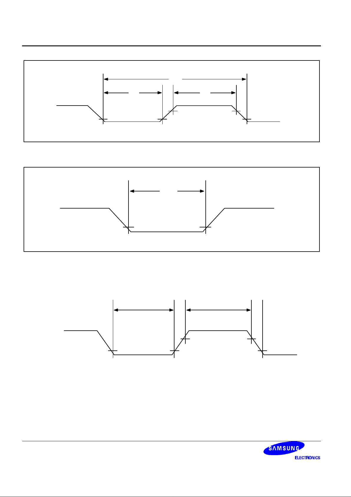
Figure 13-6. TCL0 Timing
tRSL
0.2 V
Figure 13-7. Input Timing for RESET Signal
DD
0.8 V
0.2 V
DD
DD
13–12
INT0, 1
t
INTL
0.8 V
DD
t
INTH
INTP0
0.2 V
KS0 to KS7
DD
Figure 13-8. Input Timing for External Interrupts and Quasi-Interrupts

KS57C21408/C21418/P21408 MECHANICAL DATA
14 MECHANICAL DATA
OVERVIEW
This section contains the following information about the device package:
— Package dimensions in millimeters
— Pad diagram
— Pad/pin coordinate data table
17.90 ± 0.3
14.00 ± 0.2
#100
#1
23.90 ± 0.3
20.00 ± 0.2
100-QFP-1420C
0.3 ± 0.1
0.10 MAX
0.65
(0.58)
(0.83)
0-8
0.15
0.10 MAX
0.80 ± 0.20
0.05 MIN
2.65 ± 0.10
+0.10
-0.05
NOTE: Dimensions are in millimeters.
Figure 14-1. 100-QFP-1420 Package Dimensions
3.00 MAX
0.80 ± 0.20
14-1

MECHANICAL DATA KS57C21408/C21418/P21408
NOTES
14-2

KS57C21408/C21418/P21408 KS57P21408 OTP
15 KS57P21408 OTP
OVERVIEW
The KS57P21408 single-chip CMOS microcontroller is the OTP (One Time Programmable) version of the
KS57C21408/C21418 microcontroller. It has an on-chip OTP ROM instead of masked ROM. The EPROM is
accessed by serial data format.
The KS57P21408 is fully compatible with the KS57C21408/C21418, both in function and in pin configuration.
Because of its simple programming requirements, the KS57P21408 is ideal for use as an evaluation chip for the
KS57C21408/C21418.
15-1

KS57P21408 OTP KS57C21408/C21418/P21408
SEG39
SEG40
SEG41
SEG42
SEG43
SEG44
SEG45
SEG46
SEG47
SEG48
SEG49
SEG50
SEG51
SEG52
SEG53
SEG54
SEG55
SEG56
SEG57
SEG58
81
82
83
84
85
86
87
88
89
90
91
92
93
94
95
96
97
98
99
100
SDAT
SCLK
RESET
SEG59
COM4
COM5
COM6
COM7
COM8
P6.0/KS0
P6.1/KS1
P6.2/KS2
P6.3/KS3
P7.0/KS4
P7.1/KS5
/P7.2/KS6
/P7.3/KS7
/VDD
V
DD
V
/VSS
SS
Xout
Xin
V
/
TEST
PP
XTin
XTout
/ RESET
P2.0/BUZ
P2.1/CLO
P5.0
P5.1
P5.2
P5.3
TCL0/P4.0
TCLO0/P4.1
1
2
3
4
5
6
7
8
9
10
11
12
13
14
15
16
17
18
19
20
21
22
23
24
25
26
27
28
29
30
31
32
33
34
KS57P21408
100-QFP 1420C
39
38
37
36
35
40
41
42
43
44
45
46
47
48
49
50
80
79
78
77
76
75
74
73
72
71
70
69
68
67
66
65
64
63
62
61
60
59
58
57
56
55
54
53
52
51
SEG38
SEG37
SEG36
SEG35
SEG34
SEG33
SEG32
SEG31
SEG30
SEG29
SEG28
SEG27
SEG26
SEG25
SEG24
SEG23
SEG22
SEG21
SEG20
SEG19
SEG18
SEG17
SEG16
SEG15/P8.15
SEG14/P8.14
SEG13/P8.13
SEG12/P8.12
SEG11/P8.11
SEG10/P8.10
SEG9/P8.9
COM1
COM0
INT0/P1.0
INT1/P1.1
P0.0/K0
P0.1/K1
P0.2/K2
P0.3/K3
P4.2
Figure 15-1. KS57P21408 Pin Assignments (100-QFP Package)
15-2
COM3
COM2
SEG3/P8.3
SEG2/P8.2
SEG1/P8.1
SEG0/P8.0
SEG7/P8.7
SEG6/P8.6
SEG5/P8.5
SEG4/P8.4
SEG8/P8.8

KS57C21408/C21418/P21408 KS57P21408 OTP
Table 15-1. Descriptions of Pins Used to Read/Write the EPROM
Main Chip During Programming
Pin Name Pin Name Pin No. I/O Function
P3.1 SDAT 13 I/O Serial data pin. Output port when reading and
input port when writing. Can be assigned as a
Input / push-pull output port.
P3.0 SCLK 14 I/O Serial clock pin. Input only pin.
TEST
VPP(TEST)
19 I Power supply pin for EPROM cell writing
(indicates that OTP enters into the writing
mode). When 12.5 V is applied, OTP is in writing
mode and when 5 V is applied, OTP is in reading
mode. (Option)
RESET RESET
VDD / V
SS
VDD / V
SS
22 I Chip initialization
15/16 I Logic power supply pin. VDD should be tied to
+5 V during programming.
Table 15-2. Comparison of KS57P21408 and KS57C21408/C21418 Features
Characteristic KS57P21408 KS57C21408
Program Memory 8 Kbyte EPROM 8 Kbyte mask ROM
Operating Voltage (VDD)
1.8 V to 5.5 V 1.8 V to 5.5V
OTP Programming Mode
VDD = 5 V, VPP(TEST)=12.5V
Pin Configuration 100 QFP 100 QFP
EPROM Programmability User Program 1 time Programmed at the factory
OPERATING MODE CHARACTERISTICS
When 12.5 V is supplied to the VPP(TEST) pin of the KS57P21408, the EPROM programming mode is entered.
The operating mode (read, write, or read protection) is selected according to the input signals to the pins listed in
Table 15-3 below.
Table 15-3. Operating Mode Selection Criteria
V
DD
VPP
(TEST)
REG/
MEM
ADDRESS
(A15-A0)
R/W MODE
5 V 5 V 0 0000H 1 EPROM read
12.5 V 0 0000H 0 EPROM program
12.5 V 0 0000H 1 EPROM verify
12.5 V 1 0E3FH 0 EPROM read protection
NOTE: "0" means Low level; "1" means High level.
15-3

KS57P21408 OTP KS57C21408/C21418/P21408
Table 15-4. D.C Characteristics
(TA = –40 °C to +85C, VDD = 1.8 V to 5.5V)
Parameter Symbol Conditions Min. Typ. Max. Units
Supply Current
(2)(3)
I
DD1
Run mode :
VDD=5V±10%
6MHz
– 5.1 8 mA
I
DD2
I
DD3
I
DD4
I
DD5
Crystal oscillator
C1=C2=22pF
VDD=3V±10%
Idle mode :
VDD=5V±10%
Crystal oscillator
C1=C2=22pF
VDD=3V±10%
Run mode : VDD=3V±10%
32kHz crystal oscillator
Idle mode :
VDD=3V±10%
32kHz crystal oscillator
VDD=3V±10%
32kHz crystal oscillator
Stop mode; VDD=5V±10%
4.19MHz
6MHz
4.19MHz
6MHz
4.19MHz
6MHz
4.19MHz
LCD ON
LCD OFF
3.8 6
2.5 4
1.8 3
1.3 2.5
1.1 1.8
0.5 1.5
0.4 1.0
– 30 45
(4)
– 17 30
µA
6 15
– 2.4 5
Stop mode; VDD=3V±10%
NOTES:
1. VM1=2.75/3.75 VDD, VM2=1/3.75 VDD, VM3=2/3.75 VDD, VM4=1.75/3.75 VDD
2. Supply current does not include current drawn through internal pull-down resistor and LCD driving resistors.
3. For D.C. electrical voltages, PCON register must be set to 0011B.
5. The mode of I
(LCD ON) is normal.
DD4
0.6 3
15-4

KS57C21408/C21418/P21408 KS57P21408 OTP
Main Oscillator
CPU Clock
1.5 MHz
Frequency
6 MHz
0.75 MHz
15.625 kHz
1 2 3 4 5 6 7
1.8 V
CPU CLOCK = 1/nx oscillator frequency (n = 4, 8, 64)
Supply Voltage(V)
Figure 15-2. Standard Operating Voltage Range
3 MHz
400 kHz
15-5

KS57P21408 OTP KS57C21408/C21418/P21408
NOTES
15-6
 Loading...