

Page 1
KA3502
PC SMPS Supervisory IC
www.fairchildsemi.com
Features
• Complete Housekeeping Circuit
• Few External Components
• Over Voltage Protection for 3.3V/5V/12V/Adj. Output
• Over Current Protection for 3.3V/5V/12V Output
• Open-Collector Output and Remote On/Off Function
• Remote On/Off Delay Time Control
• Precision Voltage Reference for Outputs, 5V/12V
• Uncommitment Precision Voltage Reference for +5V s
• Power Good Signal Generator with Hysteresis
• Disable Logi c of 3.3V, 5V, 12V for Complete Shutdown
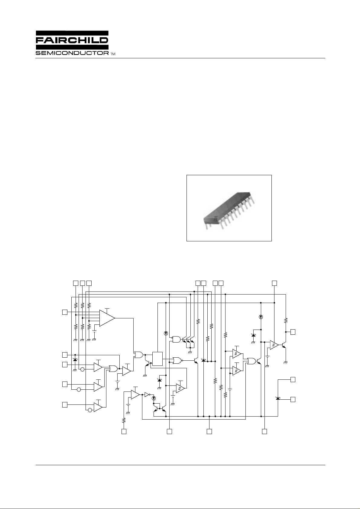
Internal Block Diagram
V33
V5 V12
123 6
Descriptions
The KA3502 is complete housekeeping circui try for use in
the secondary side of SMPS(Switched Mode Power Supply).
It contains various functions, which are two Precision Voltage References, Over Voltage/Current Protection, Remote
On/Off Control, Power Good Signal Generator, Disable
Logic and etc.
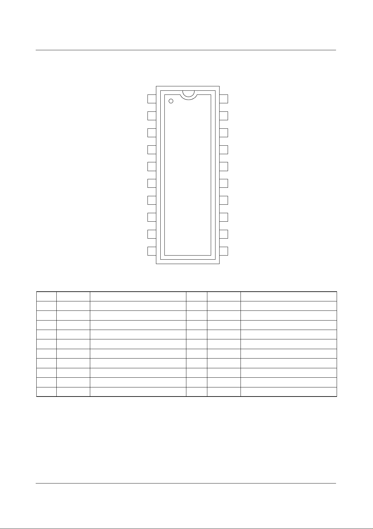
20-DIP
1
PWM FB1 VREF1 UV
14
15
11
VCC
5
R5R1R3
Vcc
+
+
+
+
R4
+
-
+
65mV
R6
1.26V
Vcc
+
-
COMP2
Vcc
+
-
COMP3
Vcc
+
-
COMP4
COMP1
-
2V
Tsur
IS33
IS12
Adj
4
R2
17
IS5
2.7V
19
-
50mV
20
-
+
135mV
18
©2000 Fairchild Semiconductor International
+
-
REM
Vcc
COMP5
1.4V
R7
Vcc
+
-
COMP6
2.8V
R8
R10
1k
39k
Ion
Vcc
S
Q
R
Vcc
+
-
↔
0.7V
Ion+
Ioff
2V
87
Trem
Q1
REFERENCE1
R11
5.4k
16
GND
R9
10k
R12
R13
R14
Vcc
+
Vcc
+
-
COMP8
1.28V
COMP7
↔
1.24V
5.2V
Ichg
Q2
REFERENCE2
10
Topr
+
-
2V
COMP9
↔
1.3V
Q3
R15
5.1k
9
PG
12
FB2
13
VREF2
Rev. 5.0
Page 2
KA3502
Pin Assignments
#1
V33
V5
V12
Adj
VCC
PWM
REM
Trem
PG
Topr
#10
K
A
3
5
0
2
#20
IS33
IS5
IS12
Tsur
GND
FB1
VREF1
VREF2
FB2
UV
#11
NO NAME FUNCTION NO NAME FUNCTION
1 V33 +3.3 V OUTPUT VOLTAGE 11 UV PG INPUT for Det
2 V5 +5 V OUTPUT VOLTAGE 12 FB2 FEEDBACK for REFERENCE 2
3 V12 +12 V OUTPUT VOLTAGE 13 VREF2 PRECISION REFERENCE
4 Adj ADJUSTABLE OVP INPUT 14 VREF1 PRECISION REFERENCE
5 VCC SUPPLY VOLTAGE 15 FB1 FEEDBACK for REFERENCE 1
6 PWM REMOTE ON/OFF OUTPUT 16 GND GROUND
7 REM REMOTE ON/OFF INPUT 17 Tsur OCP DELAY
8 Trem REMOTE ON/OFF DELAY 18 IS12 Current INPUT for +12V
9 PG POWER GOOD OUTPUT 19 IS5 Current INPUT for +5V
10 Topr PG DELAY 20 IS33 Current INPUT for +3.3V
2
Page 3
Pin Description
Pin Number Pin Name Pin Function Descrition
1 V33 +3.3 V Output Voltage of SMPS Secondary side
2 V5 +5 V Output Voltage of SMPS Secondary side
3 V12 +12 V Output Voltage of SMPS Secondary side
Adjustable OVP Input. Its Threshold Voltage is 1.26 V. This pin can be used for
4ADJ
5 VCC Supply Voltage. Operating range is 15 V ~ 24 V. Vcc=18 V, Ta=25°C at test.
6PWM
7REM
8Trem
9PG
10 Topr
11 UV Under-Voltage Detect Pin. Its threshold voltage is 1.26V ± 20mV Typ.
12 FB2 Feedback for Precision Reference2. Absolute min/max current rating is 1 mA/30 mA.
13 VREF2
14 VREF1
15 FB1
16 GND Ground
17 Tsur
18 IS12
19 IS5 Current Sense Input for +5 V. The OCP Offset voltage for +5 V is 50 mV
20 IS33 Current Sense Input for +3.3 V. The OCP Offset voltage for +3.3 V is 135 mV
another
protection signal.
Remote On/Off Output. This signal controls the primary power switch (PWM IC)
through an Opto-coupler.
Maximum current rating is 30 mA. When PW M="Low", the main SMPS is operational
and If PWM="High", the main SMPS is turned-off.
Remote On/Off Input. It is TTL operation and its threshold voltage is 1.4 V. Voltage at
this pin can reach normally 4.6 V, with absolutely maximum voltage, 5.25 V. If
REM="Low", PWM="Low". That means the main SMPS is operational. When REM
="High", then PWM="High" and the main SMPS is turned-off.
Remote On/Off delay. Ton/Toff=8 ms/24 ms (Typ.) with Ctrem=0.1uF. Its High/Low
threshold voltage is 2 V/0.7 V and the maximum voltage after full charging is about
2.8 V. So,
∆V (Chg.) = 2 V, ∆V (Dischg.) = 2.1 V Typ.
Power Good output signal. PG="High" means that the power is "Good" for operation
and PG="Low" means "Power Fail".
PG Delay. Td=250 ms (Typ.) with Ctopr=2.2uF. The High/Low threshold voltage are
2 V/1.3 V and the voltage of PIN 10 is clamped at 5.2 V for Noise margin.
Precision Reference 2 input Voltage. This circuit equals to KA431 and it is designed
for an Auxiliary voltage,
+5 Vs. It is trimmed to ± 1.6%.
Precision Reference 1 Input Voltage. This circuit equals to KA431 and it is for
corrective output voltages of +5 V/+12 V. It's trimmed to ± 1.6%.
Feedback for Precision Reference1. Absolute min/max current rating is 2 mA/30 mA
because of
internal connection.
Timing pin for Over Current Protection blank-out time. Its threshold voltage is 2 V and
clamped at 2.7 V after full charging. Target of delay time is 20 ms~30 ms and it is
realized through external R & C.
Current Sense Input for +12V. This pin is connected to the Current Sensing resistor
or inductor. If the voltage drop of the resistor or inductor is larger than the fixed offset
voltage ( 65 mV Typ.), PWM becomes "High" after some delay and the main SMPS
is turned-off.
KA3502
3
Page 4
KA3502
Absolute Maximum Ratings
Parameter Symbol Value Unit
Supply Voltage Vcc 15 ~ 24 V
UV Input Voltage Vuv 24 V
Input Maximum Voltage Vin (max) Vcc - 3 V
Cathode Current for FB1, 2 Ik1, 2 1 ~ 30 mA
PWM Maximum Current Io (PWM) 30 mA
PG Output Maximum Current Io (PG) 30 mA
Power Dissipation Pd 1 W
Operating Temperature Range Topr 0 ~ 70 °C
Storage Temperature Range Tstg -65 ~ 150 °C
Temperature Characteristics
Parameter Symbol Value Unit
Temperature Stability for Vref1, 2
(0°C ≤ Ta ≤ 70°C)
∆Vref1, 2 17 mV
4
Page 5
KA3502
Electrical Characteristics (Vcc = 18V, Ta = 25°°°°C)
Parameter Symbol Condition Min. Typ. Max. Unit
PROTECTION SECTION
Over Voltage Protection For 3.3 V Vovp33 Pin 7 (REM)=0V 3.8 4.0 4.2 V
Over Voltage Protection For 5 V Vovp5 Pin 7 (REM)=0V 5.8 6.1 6.4 V
Over Voltage Protection For 12 V Vovp12 Pin 7 (REM)=0V 13.4 14.2 15.0 V
OVP Input Threshold Voltage for Adj Vadj Pin 7 (REM)=0V 1.22 1.26 1.30 V
Comparator Offset Voltage for 3.3 V Vos33 Pin 7 (REM)=0V 125.5 135 144.5 mV
Comparator Offset Voltage for 5 V Vos5 Pin 7 (REM)=0V 46.5 50 53.5 mV
Comparator Offset Voltage for 12 V Vos12 Pin 7 (REM)=0V 60.5 65 69.5 mV
OCP Delay Comparator Input
Threshold Voltage
Pin 17 (Tsur) Input Clamp Voltage V17max Pin 7 (REM)=0V - 2.7 4 V
REMOTE ON/OFF SECTION
Remote On/off Input Threshold Vtg. Vth Pin 7 (REM): “L”→”H” 1 - 1.8 V
Remote On/off Input Open Voltage Vih Pin 7 Open 4 - 5.25 V
Remote On/off Input Low Current Iil Pin 7 (REM)=0 V 0 - -1.0 mA
ON Delay Tim e Ton REM: “L”→“H”, C=0.1 uF 4 8 14 msec
OFF Delay Time Toff REM: “L”→“H”, C=0.1 uF 16 24 34 msec
PWM Saturation Voltage Vsat
PWM Leakage Current Ileak Pin 6 (PWM)=20 V - 0.01 1 uA
REFERENCE 1 SECTION
Reference Input Voltage 1 Vref1 IIk1=1 mA 2.46 2.50 2.54 V
Line Regulation 1 Vref1 (line) 15 V<Vcc<20 V - 1 - mV/V
Current Stability 1 ∆ Vref1 Ik1=1 mA to 10 mA - 5 20 mV
Output Sinking Current Capability 1 Isink1 - 15 25 - mA
Absolute Precision of Internal Three
Resistors
Matching Coefficient of Internal Three
Resistors
Temperature Stability ∆ Vref1 Ta=0 to 70°C (Note 1) - 13 17 mV
Gain Bandwidth 1 GBW1 GV=1 (Note 1) - 1 - MHz
Vth (Tsur) Pin 7 (REM)=0V 1.9 2 2.1 V
Io=0.5 mA - - 1.3 V
(PWM)
Rint - - ± 15 - %
Rrate - - ± 1- %
5
Page 6
KA3502
Electrical Characteristics (Continued)
Parameter Symbol Condition Min. Typ. Max. Unit
REFERENCE 2 SECTION
Reference Input Voltage 2 Vref2 IIk2=1 mA 2.46 2.50 2.54 V
Line Regulation 2 Vref2 (line) 15 V<Vcc<20 V - 1 - mV/V
Current Stability 2 ∆ Vref2 Ik2 mA to 10 mA - 5 20 mV
Output Sinking Current Capability 2 Isink2 - 15 25 - mA
Temperature Stability 2 ∆ Vref2 Ta=0 to 70°C (Note 1) - 13 17 mV
Gain Bandwidth 2 GBW2 GV=1 (Note 1) - 1 - MHz
POWER GOOD SECTION
Detecting UV Voltage Vuv Pin 7 (REM)=0V 1.22 1.26 1.30 V
Detecting V5 Voltage Vin (V5) Pin 7 (REM)=0V 4.1 4.3 4.5 V
Hysteresis Voltage 1 HY1 Pin 11 (UV): “L”↔“H” 204080mV
Hysteresis Voltage 2 HY2 Pin 10 (Topr): “L”↔ “H” 0.2 0.7 - V
High Threshold Voltage of Comp 9 Vth (H) Pin 10 (Topr): “L”↔ “H” 1.8 2.0 2.2 V
Noise margin of Vtopr ∆ Vtopr Vtopr (max) - Vth (L) 2 4 - V
Charging Current for PG Delay Ichg Pin 10 (Topr)=GND -12 -18 -28 uA
Turn-On Delay Time for PG Topr Ctopr=2.2uF 100 250 500 msec
UV Input Pull Down Resistor Ruv - - 20 - kohm
PG Output Rising Time Tr C=0.1nF (Note 1) - 1 - usec
PG Output Falling Time Tf C=0.1nF (Note 1) - 300 - nsec
PG Output Saturation Voltage Vsat (PG) Isink=15 mA - 0.3 0.4 V
PG Output Voltage at High Status Vpgh Isource=100 uA 4.2 - 5.25 V
DISABLE SECTION
Disable Saturation Voltage for V33 Vdis33 REM=2 V, Isink=10 mA - 0.2 0.4 V
Disable Saturation Voltage for V5 Vdi5 REM=2 V, Isink=10 mA - 0.2 0.4 V
Disable Saturation Voltage for V12 Vdis12 REM=2 V, Isink=10 mA - 0.2 0.4 V
TOTAL STANDBY CURRENT
Supply Current Of Vcc Icc Vcc=18 V, REM=2V - 5 10 mA
Note:
1.These parameters, although guaranteed, but not 100% tested in production.
6
Page 7
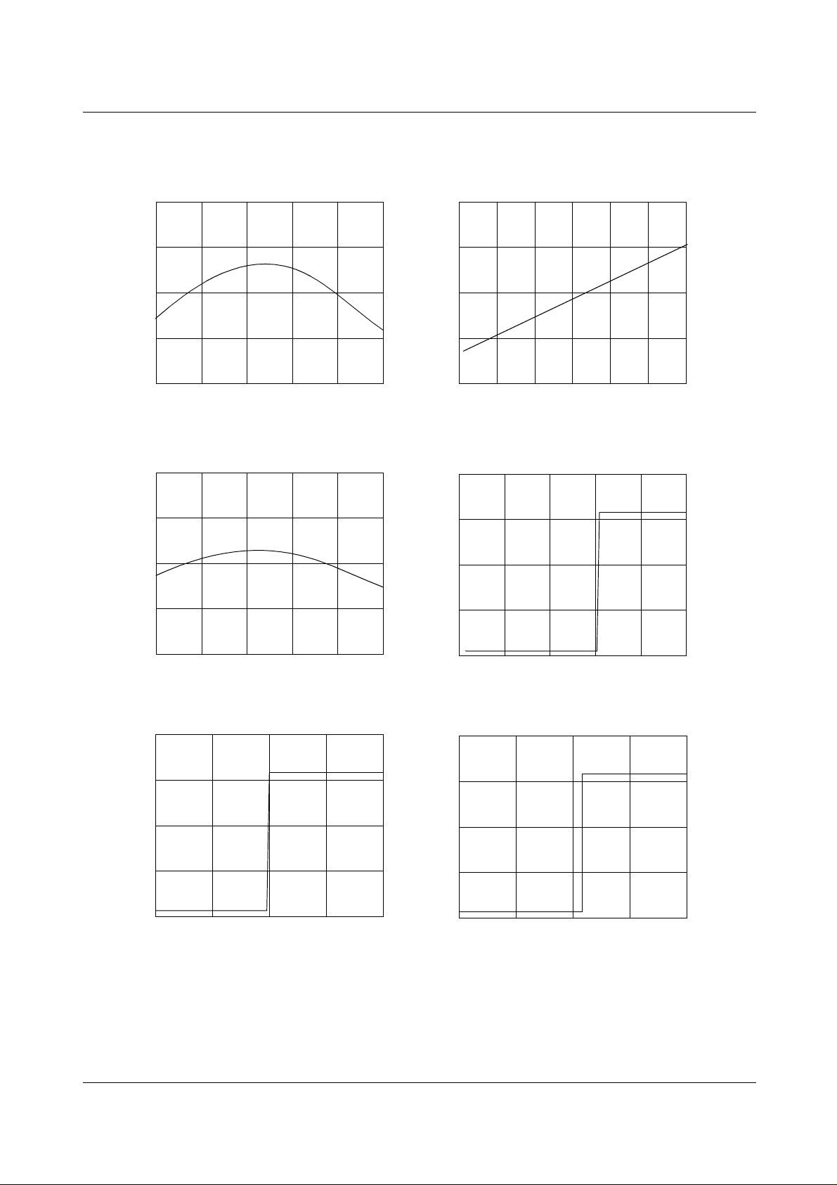
Typical Characteristics
KA3502
2.510
2.505
2.500
Vref ( V)
2.495
2.490
-25 0 25 50 75 100
Temp (Dgree)
Figure 1. Temperature Stability for Vref1,2
1.260
1.255
1.250
Vadj (V)
2.53
2.52
2.51
Vref1, 2 (V)
2.50
2.49
0 5 10 15 20 25 30
1k (mA)
Figure 2. Vref1,2 Current Stability
20
15
10
PWM (V)
1.245
1.240
-25 0 25 50 75 100
Temp (De gree)
Figure 3. Bandgap Voltage (Vadj)
20
15
10
PWM (V)
5
0
3.50 3.75 4.00 4.25 4.50
V33 (V)
Figure 3. Over Voltage Protection for +3.3V
5
0
1.10 1.15 1.20 1.25 1.30 1.35
Vadj (V)
Figure 4. OVP Input Threshold Voltage for Adj
20
15
10
PWM (V)
5
0
5.0 5.5 6.0 6.5 7.0
V5 (V)
Figure 4. OCP Offiset Voltage for 3.3V
7
Page 8

KA3502
Typical Cha ra cte ri sti c s (C o ntinued)
20
15
10
PWM (V)
5
0
12 13 14 15 16
V12 (V)
Figure 7. Over Voltage Protection for +12V
20
Vos5=IS5-V5
15
10
PWM (V)
5
20
15
10
PWM (V)
5
0
110 120 130 140 150
Vos33 (mV)
Figure 8. OCP Offiset Voltage for 3.3V
20
Vos=IS12-Vo12
15
10
PWM (V)
5
Vos33=IS33-V33
0
40 45 50 55 60
Vos5 (m V)
Figure 9. OCP Offiset Voltage for 5V
20
15
10
PWM (V)
5
0
0.0 0.5 1.0 1.5 2.0
Vth (V)
Figure 11. Remotr On/Off Input Threshold
0
55 60 65 70 75
V8 (V)
Figure 10. OCP Offiset Voltage for 12V
20
15
10
PWM (V)
5
0
0.0 0.5 1.0 1.5 2.0 2.5
V8 (V)
Figure 12. ON/OFF Delay Threshold Voltage
8
Page 9

Typical Cha ra cte ri sti c s (C o ntinued)
KA3502
25
20
15
10
PWM (V)
5
0
0 5 10 15 20
Isink (mA)
Figure 13. PWM Saturation Voltage
5
4
3
PG (V)
2
6
5
4
3
PG (V)
2
1
0
1.20 1.22 1.24 1.26 1.28 1.30
Vuv (V)
Figure 14. Detecting UV Voltage
5
4
3
PG (V)
2
1
0
5.0 4.8 4.6 4.4 4.2 4.0
V5 (V)
Figure 15. Detecting V5 Voltage for PG
0.4
0.3
0.2
Vsat_PG (V)
0.1
0.0
0 5 10 15 20 25
Isink (mA)
Figure 17. PG Saturating Voltage
1
0
0.5 1.0 1.5 2.0 2.5
V10 (V)
Figure 16. High/low Threshold Voltage of Comp9
0.4
0.3
0.2
Vdis (V)
0.1
0.0
0 5 10 15 20
Isink (mA)
Figure 18. Disable Saturation Voltage
9
Page 10

KA3502
Typical Cha ra cte ri sti c s (C o ntinued)
10
8
6
4
Icc (mA)
2
0
14 16 18 20 22
Vcc (V)
Figure 19. Supply Current of Vcc
6
5
4
3
(V)
2
UV
PG
20
15
10
(V)
5
24
0
020406080100
REM
PWM
Time (msec )
Figure 20.
1
0
0.0 0.2 0.4 0.6 0.8 1.0
Time (s ec)
Figure 21. PG Delay
10
Page 11

Mechanical Dimensions
Package
KA3502
Dimensions in millimeters
20-DIP
11
Page 12

KA3502
Ordering Information
Product Number Package Operating Temperature
KA3502 20-DIP 0°C ~ 70°C
12
Page 13

KA3502
13
Page 14

KA3502
DISCLAIMER
FAIRCHILD SEMICONDUCTOR RESERVES THE RIGHT TO MAKE CHANGES WITHOUT FURT HER NOTICE TO ANY
PRODUCTS HEREI N TO IMPROVE RELIABILITY, FUNCTIO N OR DESIGN. FAIRCH IL D DOES NOT ASSUME ANY
LIABILITY ARISING OUT OF THE APPLICATION OR USE OF ANY PRODUCT OR CIRCUIT DESCRIBED HEREIN; NEITHER
DOES IT CONVEY ANY LICENSE UNDER IT S PATENT RIGHTS, NOR THE RIGHTS OF OTHE RS.
LIFE SUPPORT POL I CY
FAIRCHILD’S PR ODUCTS ARE NOT AUTH ORIZED FOR USE AS C RITICAL COMPONENT S IN LIFE SUPPORT DE VICES
OR SYSTEMS WITHOUT THE EXPRESS WRITTEN APPROVAL OF THE PRESIDENT OF FAIRCHILD SEMICONDUCTOR
INTERNATIONAL. As used herein:
1. Life support devices or systems are devices or systems
which, (a) are intended for surgical implant into the body,
or (b) support or sustain life, and (c) whose failure to
perform when properly used in accordance with
2. A critical component in any component of a life support
device or sy stem whose fai lure to perform can be
reasonably expec ted to cause the failur e of the life support
device or system, or to affect its safety or effec t iv ene ss .
instructions for use provided in the labeling, can be
reasonably expected to result in a significant injury of the
user.
www.fairchildsemi.com
9/25/00 0.0m 001
2000 Fairchild Semiconductor International
Stock#DSxxxxxxxx
 Loading...