

Page 1

ISP1107
Advanced Universal Serial Bus transceiver
Rev. 01 — 23 February 2000 Objective specification
1. General description
The ISP1107 is a Universal Serial Bus (USB) transceiver that is fully compliant with
the
Universal Serial Bus Specification Rev. 1.1
devices such as mobile phones, digital still cameras and personal digital assistants. It
allows 1.8 V, 2.5 V and 3.3 V USB Application Specific ICs (ASICs) and
Programmable Logic Devices (PLDs) to interface with the physical layer of the
Universal Serial Bus. It has an integrated 5 V to 3.3 V voltage regulator allowing
direct powering from the USB supply V
The ISP1107 can be used as a USB device transceiver or a USB host transceiver. It
can transmit and receive serial data at both full-speed (12 Mbit/s) and low-speed
(1.5 Mbit/s) data rates. The ISP1107 is compatible with the industry-standard Philips
Semiconductors USB transceiver PDIUSBP11A.
BUS
. It is ideal for portable electronics
.
2. Features
■ Complies with
■ Integrated 5 V to 3.3 V voltage regulator allowing direct powering from USB V
c
c
■ Used as a USB device transceiver or a USB host transceiver
■ Supports full-speed (12 Mbit/s) and low-speed (1.5 Mbit/s) serial data rates
■ Slew-rate controlled differential data driver
■ Differential input receiver with wide common-mode range and very high input
sensitivity
■ Stable RCV output during SE0 condition
■ Two single-ended receivers with hysteresis
■ Low-power operation
■ Three I/O voltage levels: 1.8 V, 2.5 V and 3.3 V
■ Backward compatible with PDIUSBP11A
■ Higher than 8 kV ESD protection
■ Full industrial operating temperature range −40 to +85 °C
■ Available in small TSSOP16 and BCC16 packages.
Universal Serial Bus Specification Rev. 1.1
BUS
Page 2
Philips Semiconductors
ISP1107
Advanced USB transceiver
3. Applications
■ Portable electronic devices, such as
◆ mobile phones
◆ digital still cameras
◆ personal digital assistants (PDA)
◆ Internet appliances (IA).
4. Ordering information
Table 1: Ordering information
Type number Package
Name Description Version
[1]
ISP1107xx BCC16
ISP1107DH TSSOP16 plastic thin shrink small outline package; 16 leads; body width 4.4 mm SOT403-1
[1] In development.
plastic bottom chip carrier; 16 terminals; body 3 x 3 x 0.65 mm SOTxxx
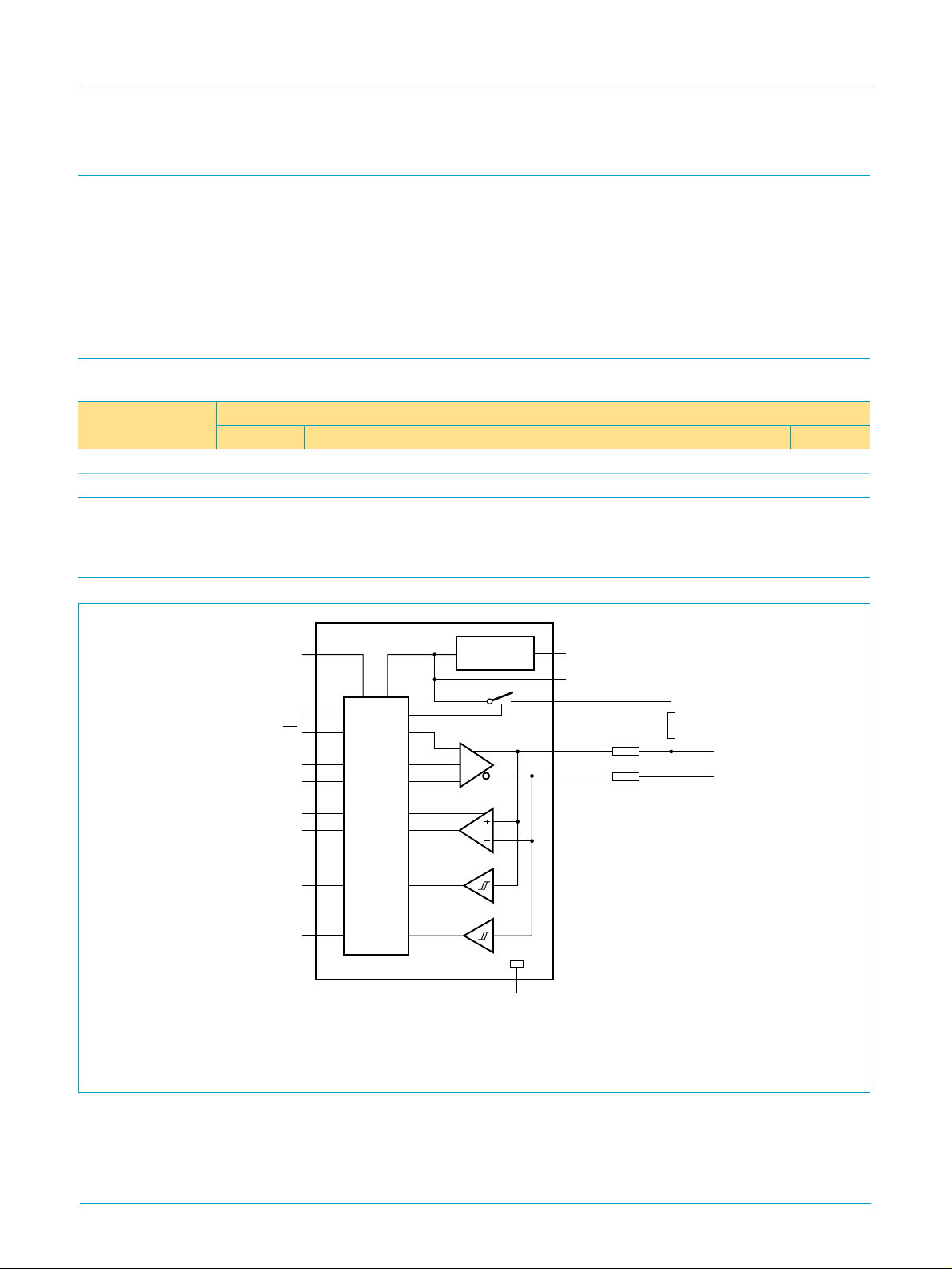
5. Functional diagram
handbook, full pagewidth
V
CC(I/O)
SOFTCON
OE
FSE0
VO
SUSPND
RCV
VP
VM
LEVEL
SHIFTER
3.3 V
ISP1107
VOLTAGE
REGULATOR
GND
V
CC(5.0)
V
reg(3.3)
V
pu(3.3)
D+
D−
MGS962
33 Ω
33 Ω
(1)
(1)
(1%)
(1%)
1.5 kΩ
(2)
(1) Use a 39 Ω resistor (1%) for a USB v2.0 compliant output impedance range.
(2) Connect to D− for low-speed operation.
Fig 1. Functional diagram.
9397 750 06899
Objective specification Rev. 01 — 23 February 2000 2 of 19
© Philips Electronics N.V. 2000. All rights reserved.
Page 3
Philips Semiconductors
6. Pinning information
6.1 Pinning
ISP1107
Advanced USB transceiver
page
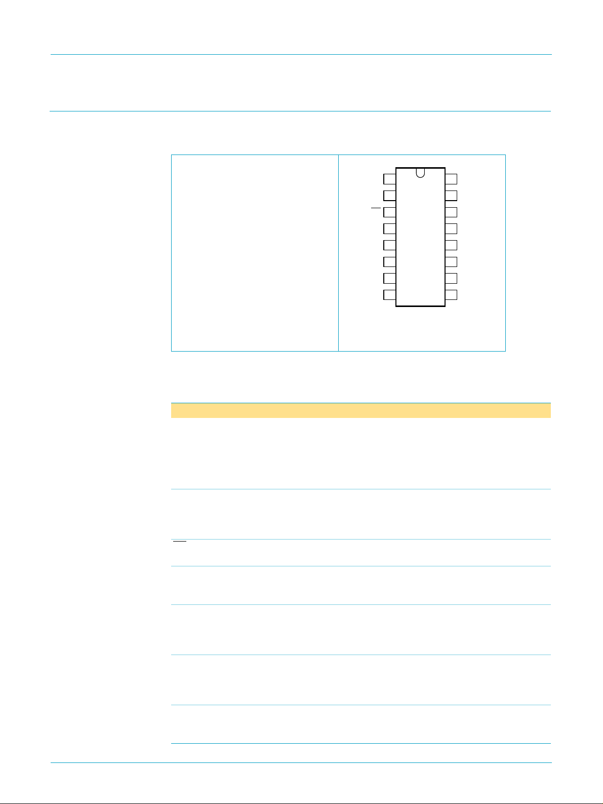
Fig 2. Pinning diagram BCC16
V
SOFTCON
SUSPND
Fig 3. Pinning diagram TSSOP16.
pu(3.3)
OE
RCV
VP
VM
GND
1
2
3
4
ISP1107DH
5
6
7
8
16
15
14
13
12
11
10
9
MGS961
(to be added).
6.2 Pin description
Table 2: Pin description
Symbol Pin Type Description
V
pu(3.3)
SOFTCON 2 I software controlled USB connection input; a HIGH level
OE 3 I output enable input (CMOS level re. V
RCV 4 O differential data receiver output (CMOS level re. V
VP 5 O single-ended D+ receiver output (CMOS level re. V
VM 6 O single-ended D− receiver output (CMOS level re. V
SUSPND 7 I suspend input (CMOSlevel re.V
1 - pull-up supply voltage (3.3 V ± 10%); used to connect an
external 1.5 kΩ resistor on D+ (full-speed) or D− (low-speed);
pin function is controlled by input SOFTCON:
SOFTCON = LOW — V
SOFTCON = HIGH — V
applies 3.3 V to pin V
pu(3.3)
floating (high impedance)
pu(3.3)
= 3.3 V
pu(3.3)
, which is connected to an external
1.5 kΩ pull-up resistor; this allows USB connect/disconnect
signalling to be controlled by software
enables the transceiver to transmit data on the USB bus
CC(I/O)
driven LOW when input SUSPND is HIGH; the output state of
RCV is preserved and stable during an SE0 condition
used for external detection of single-ended zero (SE0), error
conditions, speed of connected device; driven HIGH when
V
CC(5.0)/Vreg(3.3)
are not connected to any voltage supply
used for external detection of single-ended zero (SE0), error
conditions, speed of connected device; driven HIGH when no
supply voltage is connected to V
or V
CC(5.0)
); a HIGHlevel enables
CC(I/O)
low-power state while the USB bus is inactive and drives
output RCV to a LOW level
V
CC(5.0)
V
reg(3.3)
FSE0
VO
D+
D−
SPEED
V
CC(I/O)
, active LOW);
reg(3.3)
CC(I/O)
CC(I/O)
CC(I/O)
);
);
);
9397 750 06899
Objective specification Rev. 01 — 23 February 2000 3 of 19
© Philips Electronics N.V. 2000. All rights reserved.
Page 4

Philips Semiconductors
ISP1107
Advanced USB transceiver
Table 2: Pin description
…continued
Symbol Pin Type Description
GND 8 - ground supply
V
CC(I/O)
9 - supply voltage for digital I/O pins (1.65 to 3.6 V). Three
voltage levels are supported: 1.8 V ± 0.15 V, 2.5 V ± 0.2 V
and 3.3 V ± 0.3V; when V
is not connected, the D+/D−
CC(I/O)
pins are in three-state
SPEED 10 I speed selection input (CMOS level re. V
CC(I/O)
); adjusts the
slew rate of differential data outputs D+ and D− according to
the transmission speed:
LOW: low-speed (1.5 Mbit/s)
HIGH: full-speed (12 Mbit/s)
D− 11 AI/O negative USB data bus connection (analog, differential); for
low-speed mode connect to pin V
via a 1.5 kΩ resistor
pu(3.3)
D+ 12 AI/O positive USB data bus connection (analog, differential); for
full-speed mode connect to pin V
VO 13 I differential driver data input (CMOS level re. V
via a 1.5 kΩ resistor
pu(3.3)
CC(I/O)
, Schmitt
trigger); see Table 4
FSE0 14 I differential driver data input (CMOS level re. V
CC(I/O)
, Schmitt
trigger); see Table 4
V
reg(3.3)
15 - regulated supply voltage output (3.0 to 3.6 V) during 5 V
operation; used as supply voltage input for 3.3 V operation
(3.3 V ± 10%)
V
CC(5.0)
16 - supply voltage for 5 V operation (4.0 to 5.5 V); can be
connected directly to USB supply V
during 3.3 V operation
V
reg(3.3)
; connect this pin to
BUS
7. Functional description
7.1 Function selection
Table 3: Function table
SUSPND OE D+/D− RCV VP/VM Function
L L driving &
receiving
L H receiving
H L driving inactive
H H high-Z
[1] Signal levels on D+/D− are determined by other USB devices and external pull-up/down resistors.
[2] In ‘suspend’ mode (SUSPND = HIGH) the differential receiver is inactive and output RCV is always
LOW. Out-of-suspend (‘K’) signalling is detected via the single-ended receivers VP and VM.
[3] During suspend, the slew-rate control circuit of low-speed operation is disabled. The D+/D− are still
driven to their intended states, without slew-rate control. This is permitted because driving during
suspend is used to signal remote wakeup by driving a ‘K’ signal (one transition from idle to ‘K’ state)
for a period of 1 to 15 ms.
9397 750 06899
Objective specification Rev. 01 — 23 February 2000 4 of 19
[1]
active active normal driving
(differential receiver active)
[1]
active active receiving
[2]
active driving during ‘suspend’
(differential receiver inactive)
inactive
[2]
active low-power state
© Philips Electronics N.V. 2000. All rights reserved.
[3]
Page 5

Philips Semiconductors
7.2 Operating functions
Table 4: Driving function (OE = L)
ISP1107
Advanced USB transceiver
FSE0 VO Data
L L differential logic 0
L H differential logic 1
H L SE0
H H SE0
Table 5: Receiving function (
D+/D− RCV VP VM
differential logic 0 L L H
differential logic 1 H H L
SE0 RCV*
[1] RCV* denotes the signal level on output RCV just before SE0 state occurs. This level is kept stable
during the SE0 period.
OE=H)
[1]
LL
7.3 Power supply configurations
The ISP1107 can be used with different power supply configurations, which can be
changed dynamically. An overview is given in Table 6.
Normal mode — Both V
operation, V
is connected to a 5 V source (4.0 to 5.5 V). The internal voltage
CC(5.0)
regulator then produces 3.3 V for the USB connections. For 3.3 V operation, both
V
CC(5.0)
and V
are connected to a 3.3 V source (3.0 - 3.6 V). V
reg(3.3)
independently connected to a 1.8 V, 2.5 V or 3.3 V source, depending on the supply
voltage of the external circuit.
Disable mode — V
CC(I/O)
mode, the ISP1107’s internal circuits ensure that the D+/D− pins are in three-state
and the power consumption drops to the low-power (suspended) state level.
and V
CC(I/O)
CC(5.0)/Vreg(3.3)
is not connected, V
are connected. For 5 V
CC(5.0)/Vreg(3.3)
are connected. In this
CC(I/O)
is
Sharing mode — V
is connected, V
CC(I/O)
CC(5.0)/Vreg(3.3)
are not connected. In this
mode, the D+/D− pins are made three-state and the ISP1107 allows external signals
of up to 3.6 V to share the D+/D− lines. The ISP1107’s internal circuits ensure that
virtually no current is drawn via the D+/D− lines. The power consumption through pin
V
drops to the low-power (suspended) state level. Both the VP and VM pins are
CC(I/O)
driven HIGH to indicate this mode.
Table 6: Power supply configuration overview
V
CC(5.0)/Vreg(3.3)
connected connected Normal mode connected not connected Disable mode D+/D− high impedance
not connected connected Sharing mode D+/D− are high impedance;
9397 750 06899
Objective specification Rev. 01 — 23 February 2000 5 of 19
V
CC(I/O)
Configuration Special characteristics
VP/VM are driven HIGH
© Philips Electronics N.V. 2000. All rights reserved.
Page 6

Philips Semiconductors
ISP1107
Advanced USB transceiver
8. Limiting values
Table 7: Absolute maximum ratings
In accordance with the Absolute Maximum Rating System (IEC 60134).
Symbol Parameter Conditions Min Max Unit
V
CC(5.0)
V
CC(I/O)
V
reg(3.3)
V
I
I
latchup
V
esd
T
stg
[1] Equivalent to discharging a 100 pF capacitor via a 1.5 kΩ resistor (Human Body Model).
supply voltage −0.5 +6.0 V
I/O supply voltage −0.5 +4.6 V
regulated supply voltage −0.5 +4.6 V
DC input voltage −0.5 V
CC(I/O)
+ 0.5 V
latchup current VI=−1.8 to 5.4 V - 100 mA
electrostatic discharge voltage
[1]
ILI<1µA
pins D+, D− - ±8000 V
other pins - ±2000 V
storage temperature −40 +125 °C
Table 8: Recommended operating conditions
Symbol Parameter Conditions Min Typ Max Unit
V
CC(5.0)
V
CC(I/O)
V
reg(3.3)
V
I
V
I(AI/O)
supply voltage 5 V operation 4.0 5.0 5.5 V
I/O supply voltage 1.65 - 3.6 V
regulated supply voltage 3.3 V operation 3.0 3.3 3.6 V
input voltage 0 - V
input voltage on analog I/O
0 - 3.6 V
CC(I/O)
V
pins (D+/D−)
T
amb
operating ambient temperature −40 - +85 °C
9397 750 06899
Objective specification Rev. 01 — 23 February 2000 6 of 19
© Philips Electronics N.V. 2000. All rights reserved.
Page 7

Philips Semiconductors
ISP1107
Advanced USB transceiver
9. Static characteristics
Table 9: Static characteristics: supply pins
VCC= 4.0 to 5.5 V; V
Symbol Parameter Conditions Min Typ Max Unit
V
reg(3.3)
I
CC
I
CC(idle)
regulated supply voltage unloaded 3.0
operating supply current full-speed transmitting and receiving
supply current during
full-speed idle and SE0
I
CC(susp)
I
CC(dis)
suspend supply current SUSPND = HIGH
disable mode supply current V
ICC(I/O) operating I/O supply current full-speed transmittingand receiving
I
CC(I/O)(static)
I
CC(I/O)(sharing
static I/O supply current full-speed idle, SE0 or suspend - - 10 µA
) sharing mode I/O supply
current
I
Dx(sharing
) sharing mode load current
on pins D+ and D−
= 1.65 to 3.6 V; V
CC(I/O)
=0V; T
GND
at 12 Mbit/s; C
=−40 to+85°C; unless otherwise specified.
amb
= 50 pF on D+/D−
L
full-speed idle: D+ > 2.7 V,
D− < 0.3 V; SE0: D+ < 0.3 V,
D− < 0.3 V
not connected
CC(I/O)
at 12 Mbit/s
V
CC(5.0)/Vreg(3.3)
V
CC(5.0)/Vreg(3.3)
SOFTCON = LOW; V
not connected
not connected;
= 3.6 V
Dx
[1]
3.3 3.6 V
-610
[3]
- - 500 µA
[3]
--20µA
[3]
--20µA
- 0.3 1
[3]
--10µA
[3]
--5µA
[2]
mA
[2]
mA
[1] In ‘suspend’ mode, the minimum voltage is 2.7 V.
[2] Characterized only, not tested in production.
[3] Excluding V
source current to 1.5 kΩ and 15 kΩ pull-up and pull-down resistors (200 µA typ.).
pu(3.3)
Table 10: Static characteristics: digital pins
VCC= 4.0 to 5.5 V; V
= 1.65 to 3.6 V; V
CC(I/O)
GND
=0V; T
=−40 to+85°C; unless otherwise specified.
amb
Symbol Parameter Conditions Min Typ Max Unit
V
= 1.65 to 3.6 V
CC(I/O)
Input levels
V
IL
V
IH
LOW-level input voltage - - 0.3V
HIGH-level input voltage 0.6V
CC(I/O)
-- V
CC(I/O)
V
Output levels
= 100 µA - - 0.15 V
I
V
OL
V
OH
LOW-level output voltage
HIGH-level output voltage
OL
= 4 mA - - 0.4 V
I
OL
= 100 µAV
I
OH
= 4 mA V
I
OH
− 0.15 - - V
CC(I/O)
− 0.4 - - V
CC(I/O)
Leakage current
I
LI
V
CC(I/O)
input leakage current - - ±1 µA
= 1.8 V ± 0.15 V
Input levels
V
IL
V
IH
LOW-level input voltage - - 0.5 V
HIGH-level input voltage 1.2 - - V
9397 750 06899
Objective specification Rev. 01 — 23 February 2000 7 of 19
© Philips Electronics N.V. 2000. All rights reserved.
Page 8

Philips Semiconductors
ISP1107
Advanced USB transceiver
Table 10: Static characteristics: digital pins
VCC= 4.0 to 5.5 V; V
= 1.65 to 3.6 V; V
CC(I/O)
…continued
=0V; T
GND
=−40 to+85°C; unless otherwise specified.
amb
Symbol Parameter Conditions Min Typ Max Unit
Output levels
= 100 µA - - 0.15 V
I
V
OL
V
OH
V
CC(I/O)
LOW-level output voltage
HIGH-level output voltage
= 2.5 V ± 0.2 V)
OL
= 4 mA - - 0.4 V
I
OL
= 100 µA 1.5 - - V
I
OH
= 4 mA 1.25 - - V
I
OH
Input levels
V
IL
V
IH
LOW-level input voltage - - 0.7 V
HIGH-level input voltage 1.7 - - V
Output levels
= 100 µA - - 0.15 V
I
V
OL
V
OH
V
CC(I/O)
LOW-level output voltage
HIGH-level output voltage
= 3.3 V ± 0.3 V
OL
= 4 mA - - 0.4 V
I
OL
= 100 µA 2.15 - - V
I
OH
= 4 mA 1.9 - - V
I
OH
Input levels
V
IL
V
IH
LOW-level input voltage - - 0.9 V
HIGH-level input voltage 2.15 - - V
Output levels
= 100 µA - - 0.2 V
I
V
OL
V
OH
LOW-level output voltage
HIGH-level output voltage
OL
= 4 mA - - 0.4 V
I
OL
= 100 µA 2.85 - - V
I
OH
= 4 mA 2.6 - - V
I
OH
Table 11: Static characteristics: analog I/O pins (D+, D−)
VCC= 4.0 to 5.5 V; V
= 1.65 to 3.6 V; V
CC(I/O)
GND
=0V; T
=−40 to+85°C; unless otherwise specified.
amb
Symbol Parameter Conditions Min Typ Max Unit
Input levels
Differential receiver
V
DI
V
CM
differential input sensitivity |V
differential common mode
− V
I(D+)
| 0.2 - - V
I(D−)
includes VDI range 0.8 - 2.5 V
voltage
Single-ended receiver
V
IL
V
IH
V
hys
LOW-level input voltage - - 0.8 V
HIGH-level input voltage 2.0 - - V
hysteresis voltage 0.4 - 0.7 V
Output levels
V
OL
V
OH
LOW-level output voltage RL= 1.5 kΩ to + 3.6 V - - 0.3 V
HIGH-level output voltage RL=15kΩ to GND 2.8 - 3.6 V
Leakage current
I
LZ
9397 750 06899
Objective specification Rev. 01 — 23 February 2000 8 of 19
OFF-state leakage current - - ±1 µA
© Philips Electronics N.V. 2000. All rights reserved.
Page 9

Philips Semiconductors
ISP1107
Advanced USB transceiver
Table 11: Static characteristics: analog I/O pins (D+, D−)
VCC= 4.0 to 5.5 V; V
= 1.65 to 3.6 V; V
CC(I/O)
GND
=0V; T
…continued
=−40 to+85°C; unless otherwise specified.
amb
Symbol Parameter Conditions Min Typ Max Unit
Capacitance
C
IN
transceiver capacitance pin to GND - - 20 pF
Resistance
Z
Z
DRV
DRV2
driver output impedance steady-state drive
driver output impedance for
steady-state drive
[1]
34 39 44 Ω
[2]
41 45 49 Ω
USB 2.0
Z
INP
R
SW
input impedance 10 - - MΩ
internal switch resistance at
pin V
pu(3.3)
--10Ω
Termination
[3]
V
TERM
[1] Includes external resistors of 33 Ω±1% on both D+ and D−.
[2] Includes external resistors of 39 Ω±1% on both D+ and D−. This range complies with
[3] This voltage is available at pins V
[4] In ‘suspend’ mode the minimum voltage is 2.7 V.
termination voltage for
upstream port pull-up (R
reg(3.3)
)
PU
and V
pu(3.3)
.
[4]
3.0
Universal Serial Bus Specification Rev. 2.0
- 3.6 V
.
10. Dynamic characteristics
Table 12: Dynamic characteristics: analog I/O pins (D+, D−)
VCC= 4.0 to 5.5 V; V
= 1.65 to 3.6 V; V
CC(I/O)
GND
=0V; T
[1]
=−40 to+85°C; unless otherwise specified.
amb
Symbol Parameter Conditions Min Typ Max Unit
Driver characteristics
Full-speed mode
t
FR
rise time CL= 50 to 125 pF;
10 to 90% of |V
OH
− VOL|;
4 - 20 ns
see Figure 4
t
FF
fall time CL= 50 to 125 pF;
90 to 10% of |V
OH
− VOL|;
4 - 20 ns
see Figure 4
FRFM differential rise/fall time
V
CRS
matching (t
output signal crossover
FR/tFF
)
voltage
excluding the first transition
from Idle state
excluding the first transition
from Idle state; see Figure 7
90 - 111.1 %
[2]
1.3 - 2.0 V
Low-speed mode
t
LR
rise time CL= 200 to 600 pF;
10 to 90% of |V
OH
− VOL|;
75 - 300 ns
see Figure 4
t
LF
fall time CL= 200 to 600 pF;
90 to 10% of |V
OH
− VOL|;
75 - 300 ns
see Figure 4
LRFM differential rise/fall time
matching (t
LR/tLF
)
excluding the first transition
from Idle state
80 - 125 %
9397 750 06899
Objective specification Rev. 01 — 23 February 2000 9 of 19
© Philips Electronics N.V. 2000. All rights reserved.
Page 10

Philips Semiconductors
ISP1107
Advanced USB transceiver
[1]
Table 12: Dynamic characteristics: analog I/O pins (D+, D−)
VCC= 4.0 to 5.5 V; V
= 1.65 to 3.6 V; V
CC(I/O)
GND
=0V; T
amb
Symbol Parameter Conditions Min Typ Max Unit
V
CRS
output signal crossover
voltage
excluding the first transition
from idle state; see Figure 7
Driver timing
Full-speed mode
t
PLH(drv)
t
PHL(drv)
t
PHZ
t
PLZ
t
PZH
t
PZL
driver propagation delay
(VO, FSE0 to D+,D−)
driver disable delay
OE to D+,D−)
(
driver enable delay
OE to D+,D−)
(
LOW-to-HIGH; seeFigure 7 --15ns
HIGH-to-LOW; see Figure 7 --15ns
HIGH-to-OFF; see Figure 5 --10ns
LOW-to-OFF; seeFigure 5 --10ns
OFF-to-HIGH; see Figure 5 --15ns
OFF-to-LOW; see Figure 5 --15ns
Low-speed mode
Not specified: low-speed delay timings are dominated by the slow rise/fall times t
Receiver timings (full-speed and low-speed mode)
Differential receiver
t
PLH(rcv)
t
PHL(rcv)
propagation delay
(D+,D− to RCV)
LOW-to-HIGH; seeFigure 6 --15ns
HIGH-to-LOW; see Figure 6 --15ns
Single-ended receiver
t
PLH(se)
t
PHL(se)
propagation delay
(D+,D− to VP, VM)
LOW-to-HIGH; seeFigure 6 --15ns
HIGH-to-LOW; see Figure 6 --15ns
…continued
=−40 to+85°C; unless otherwise specified.
[2]
1.3 - 2.0 V
and tLF.
LR
[1] Test circuit: see Figure 10.
[2] Characterized only, not tested. Limits guaranteed by design.
1.65 V
logic input
tFR, t
V
OH
V
OL
LR
90%
10%
90%
tFF, t
10%
LF
V
MGS963
V
0 V
OH
differential
data lines
OL
0.9 V
t
t
V
PZH
PZL
CRS
V
OH
V
OL
Fig 4. Rise and fall times. Fig 5. Timing of OE to D+, D−.
2.0 V
differential
data lines
0.8 V
V
OH
logic output
V
OL
V
CRS
t
PLH(rcv)
t
PLH(se)
0.9 V
V
CRS
t
PHL(rcv)
t
PHL(se)
0.9 V
MGS965
1.65 V
0 V
V
OH
V
logic input
differential
data lines
OL
0.9 V
t
PLH(drv)
V
CRS
Fig 6. Timing of D+, D− to RCV, VP, VM. Fig 7. Timing of VO, FSE0 to D+, D−.
0.9 V
t
PHZ
t
PLZ
−0.3 V
+0.3 V
0.9 V
t
PHL(drv)
MGS966
V
CRS
MGS964
9397 750 06899
© Philips Electronics N.V. 2000. All rights reserved.
Objective specification Rev. 01 — 23 February 2000 10 of 19
Page 11

Philips Semiconductors
11. Test information
ISP1107
Advanced USB transceiver
33 Ω
test point
(1)
500 Ω
50 pF
V = 0 V for t
V=V
reg(/3.3)
handbook, halfpage
, t
PZH
PHZ
for t
, t
PZL
PLZ
D.U.T.
(1) Complies with USB 1.1. For USB 2.0 a resistor of 39 Ω must be used.
Fig 8. Load for enable and disable times.
handbook, halfpage
D.U.T.
test point
25 pF
MGS968
Fig 9. Load for VM, VP and RCV.
handbook, halfpage
V
pu(3.3)
V
MBL142
(1)
D.U.T.
1.5 kΩ
D+/D−
33 Ω
test point
(2)
C
L
Load capacitance:
CL= 50 pF or 125 pF (full-speed mode, minimum or maximum timing)
CL= 200 pF or 600 pF (low-speed mode, minimum or maximum timing)
(1) Full-speed mode: connected to D+, low-speed mode: connected to D−.
(2) Complies with USB 1.1. For USB 2.0 a resistor of 39 Ω must be used.
Fig 10. Load for D+, D−.
15 kΩ
MGS967
9397 750 06899
© Philips Electronics N.V. 2000. All rights reserved.
Objective specification Rev. 01 — 23 February 2000 11 of 19
Page 12

Philips Semiconductors
12. Package outline
Fig 11. BCC16 package outline (to be added).
ISP1107
Advanced USB transceiver
9397 750 06899
Objective specification Rev. 01 — 23 February 2000 12 of 19
© Philips Electronics N.V. 2000. All rights reserved.
Page 13

Philips Semiconductors
ISP1107
Advanced USB transceiver
TSSOP16: plastic thin shrink small outline package; 16 leads; body width 4.4 mm
D
c
y
Z
16
pin 1 index
9
A
2
18
w M
b
e
p
A
1
E
H
E
L
detail X
SOT403-1
A
X
v M
A
Q
(A )
3
A
θ
L
p
0 2.5 5 mm
scale
DIMENSIONS (mm are the original dimensions)
UNIT A1A2A
Notes
1. Plastic or metal protrusions of 0.15 mm maximum per side are not included.
2. Plastic interlead protrusions of 0.25 mm maximum per side are not included.
A
max.
0.15
mm
1.10
OUTLINE
VERSION
SOT403-1 MO-153
0.05
0.95
0.80
IEC JEDEC EIAJ
0.25
b
3
p
0.30
0.19
(1)E(2) (1)
cD
0.2
5.1
0.1
4.9
REFERENCES
eHELLpQZywv θ
4.5
4.3
0.65
6.6
6.2
0.75
0.50
0.4
0.3
EUROPEAN
PROJECTION
0.13 0.10.21.0
0.40
0.06
ISSUE DATE
95-04-04
99-12-27
o
8
o
0
Fig 12. TSSOP16 package outline.
9397 750 06899
Objective specification Rev. 01 — 23 February 2000 13 of 19
© Philips Electronics N.V. 2000. All rights reserved.
Page 14

Philips Semiconductors
13. Soldering
13.1 Introduction to soldering surface mount packages
This text gives a very brief insight to a complex technology. A more in-depth account
of soldering ICs can be found in our
Packages
There is no soldering method that is ideal for all surface mount IC packages. Wave
soldering is not always suitable for surface mount ICs, or for printed-circuit boards
with high population densities. In these situations reflow soldering is often used.
13.2 Reflow soldering
Reflow soldering requires solder paste (a suspension of fine solder particles, flux and
binding agent) to be applied to the printed-circuit board by screen printing, stencilling
or pressure-syringe dispensing before package placement.
Several methods exist for reflowing; for example, infrared/convection heating in a
conveyor type oven. Throughput times (preheating, soldering and cooling) vary
between 100 and 200 seconds depending on heating method.
ISP1107
Advanced USB transceiver
Data Handbook IC26; Integrated Circuit
(document order number 9398 652 90011).
Typical reflow peak temperatures range from 215 to 250 °C. The top-surface
temperature of the packages should preferable be kept below 230 °C.
13.3 Wave soldering
Conventional single wave soldering is not recommended for surface mount devices
(SMDs) or printed-circuit boards with a high component density, as solder bridging
and non-wetting can present major problems.
To overcome these problems the double-wave soldering method was specifically
developed.
If wave soldering is used the following conditions must be observed for optimal
results:
Use a double-wave soldering method comprising a turbulent wave with high
•
upward pressure followed by a smooth laminar wave.
For packages with leads on two sides and a pitch (e):
•
– larger than or equal to 1.27 mm, the footprint longitudinal axis is preferred to be
parallel to the transport direction of the printed-circuit board;
– smaller than 1.27 mm, the footprint longitudinal axis must be parallel to the
transport direction of the printed-circuit board.
The footprint must incorporate solder thieves at the downstream end.
For packages with leads on four sides, the footprint must be placed at a 45° angle
•
to the transport direction of the printed-circuit board. The footprint must
incorporate solder thieves downstream and at the side corners.
During placement and before soldering, the package must be fixed with a droplet of
adhesive. The adhesive can be applied by screen printing, pin transfer or syringe
dispensing. The package can be soldered after the adhesive is cured.
9397 750 06899
Objective specification Rev. 01 — 23 February 2000 14 of 19
© Philips Electronics N.V. 2000. All rights reserved.
Page 15

Philips Semiconductors
Typical dwell time is 4 seconds at 250 °C. A mildly-activated flux will eliminate the
need for removal of corrosive residues in most applications.
13.4 Manual soldering
Fix the component by first soldering two diagonally-opposite end leads. Use a low
voltage (24 V or less) soldering iron applied to the flat part of the lead. Contact time
must be limited to 10 seconds at up to 300 °C.
When using a dedicated tool, all other leads can be soldered in one operation within
2 to 5 seconds between 270 and 320 °C.
13.5 Package related soldering information
Table 13: Suitability of surface mount IC packages for wave and reflow soldering
Package Soldering method
BGA, LFBGA, SQFP, TFBGA not suitable suitable
HBCC, HLQFP, HSQFP, HSOP, HTQFP,
HTSSOP, SMS
PLCC
LQFP, QFP, TQFP not recommended
SSOP, TSSOP, VSO not recommended
ISP1107
Advanced USB transceiver
methods
Wave Reflow
not suitable
[3]
, SO, SOJ suitable suitable
[2]
[3] [4]
[5]
suitable
suitable
suitable
[1]
[1] All surface mount (SMD) packages are moisture sensitive. Depending upon the moisture content, the
maximum temperature (with respect to time) and body size of the package, there is a risk that internal
or external package cracks may occur due to vaporization of the moisture in them (the so called
popcorn effect). For details, refer to the Drypack information in the
Circuit Packages; Section: Packing Methods
[2] These packages are not suitable for wave soldering as a solder joint between the printed-circuit board
and heatsink (at bottom version) can not be achieved, and as solder may stick to the heatsink (on top
version).
[3] If wave soldering is considered, then the package must be placed at a 45° angle to the solder wave
direction. The package footprint must incorporate solder thieves downstream and at the side corners.
[4] Wave soldering is only suitable for LQFP, QFP and TQFP packages with a pitch (e) equal to or larger
than 0.8 mm; it is definitely not suitable for packages with a pitch (e) equal to or smaller than 0.65 mm.
[5] Wave soldering is only suitable for SSOP and TSSOP packages with a pitch (e) equal to or larger than
0.65 mm; it is definitely not suitable for packages with a pitch (e) equal to or smaller than 0.5 mm.
.
Data Handbook IC26; Integrated
9397 750 06899
Objective specification Rev. 01 — 23 February 2000 15 of 19
© Philips Electronics N.V. 2000. All rights reserved.
Page 16

Philips Semiconductors
14. Revision history
Table 14: Revision history
Rev Date CPCN Description
01 20000223 Objective specification; initial version.
ISP1107
Advanced USB transceiver
9397 750 06899
Objective specification Rev. 01 — 23 February 2000 16 of 19
© Philips Electronics N.V. 2000. All rights reserved.
Page 17

Philips Semiconductors
15. Data sheet status
ISP1107
Advanced USB transceiver
Datasheet status Product status Definition
Objective specification Development This data sheet contains the design target or goal specifications for product development. Specification may
change in any manner without notice.
Preliminary specification Qualification This data sheet contains preliminary data, and supplementary data will be published at a later date. Philips
Semiconductors reserves the right to make changes at any time without notice in order to improve design and
supply the best possible product.
Product specification Production This data sheet contains final specifications. Philips Semiconductors reserves the right to make changes at any
time without notice in order to improve design and supply the best possible product.
[1] Please consult the most recently issued data sheet before initiating or completing a design.
16. Definitions
Short-form specification — The data in a short-form specification is
extracted from a full data sheet with the same type number and title. For
detailed information see the relevant data sheet or data handbook.
Limiting values definition — Limiting values given are in accordance with
the Absolute Maximum Rating System (IEC 60134). Stress above one or
more of the limiting values may cause permanent damage to the device.
These are stress ratings only and operation of the device at these or at any
other conditions above those given in the Characteristics sections of the
specification is not implied. Exposure to limiting values for extended periods
may affect device reliability.
Application information — Applications that are described herein for any
of these products are for illustrative purposes only. Philips Semiconductors
make no representation or warranty that such applications will be suitable for
the specified use without further testing or modification.
[1]
17. Disclaimers
Life support — These products are not designed for use in life support
appliances, devices, or systems where malfunction of these products can
reasonably be expected to result in personal injury. Philips Semiconductors
customers using or selling these products for use in such applications do so
at their own risk and agree to fully indemnify Philips Semiconductors for any
damages resulting from such application.
Right to make changes — Philips Semiconductors reserves the right to
make changes, without notice, in the products, including circuits, standard
cells, and/or software, described or contained herein in order to improve
design and/or performance. Philips Semiconductors assumes no
responsibility or liability for the use of any of these products, conveys no
licence or title under any patent, copyright, or mask work right to these
products, and makes no representations or warranties that these products
are free from patent, copyright, or mask work right infringement, unless
otherwise specified.
9397 750 06899
© Philips Electronics N.V. 2000 All rights reserved.
Objective specification Rev. 01 — 23 February 2000 17 of 19
Page 18

Philips Semiconductors
Advanced USB transceiver
Philips Semiconductors - a worldwide company
ISP1107
Argentina: see South America
Australia: Tel. +61 2 9704 8141, Fax. +61 2 9704 8139
Austria: Tel. +43 160 101, Fax. +43 160 101 1210
Belarus: Tel. +375 17 220 0733, Fax. +375 17 220 0773
Belgium: see The Netherlands
Brazil: see South America
Bulgaria: Tel. +359 268 9211, Fax. +359 268 9102
Canada: Tel. +1 800 234 7381
China/Hong Kong: Tel. +852 2 319 7888, Fax. +852 2 319 7700
Colombia: see South America
Czech Republic: see Austria
Denmark: Tel. +45 3 288 2636, Fax. +45 3 157 0044
Finland: Tel. +358 961 5800, Fax. +358 96 158 0920
France: Tel. +33 14 099 6161, Fax. +33 14 099 6427
Germany: Tel. +49 40 23 5360, Fax. +49 402 353 6300
Hungary: see Austria
India: Tel. +91 22 493 8541, Fax. +91 22 493 8722
Indonesia: see Singapore
Ireland: Tel. +353 17 64 0000, Fax. +353 17 64 0200
Israel: Tel. +972 36 45 0444, Fax. +972 36 49 1007
Italy: Tel. +39 039 203 6838, Fax +39 039 203 6800
Japan: Tel. +81 33 740 5130, Fax. +81 3 3740 5057
Korea: Tel. +82 27 09 1412, Fax. +82 27 09 1415
Malaysia: Tel. +60 37 50 5214, Fax. +60 37 57 4880
Mexico: Tel. +9-5 800 234 7381
Middle East: see Italy
Netherlands: Tel. +31 40 278 2785, Fax. +31 40 278 8399
New Zealand: Tel. +64 98 49 4160, Fax. +64 98 49 7811
Norway: Tel. +47 22 74 8000, Fax. +47 22 74 8341
Philippines: Tel. +63 28 16 6380, Fax. +63 28 17 3474
Poland: Tel. +48 22 5710 000, Fax. +48 22 5710 001
Portugal: see Spain
Romania: see Italy
Russia: Tel. +7 095 755 6918, Fax. +7 095 755 6919
Singapore: Tel. +65 350 2538, Fax. +65 251 6500
Slovakia: see Austria
Slovenia: see Italy
South Africa: Tel. +27 11 471 5401, Fax. +27 11 471 5398
South America: Tel. +55 11 821 2333, Fax. +55 11 829 1849
Spain: Tel. +34 33 01 6312, Fax. +34 33 01 4107
Sweden: Tel. +46 86 32 2000, Fax. +46 86 32 2745
Switzerland: Tel. +41 14 88 2686, Fax. +41 14 81 7730
Taiwan: Tel. +886 22 134 2865, Fax. +886 22 134 2874
Thailand: Tel. +66 27 45 4090, Fax. +66 23 98 0793
Turkey: Tel. +90 216 522 1500, Fax. +90 216 522 1813
Ukraine: Tel. +380 44 264 2776, Fax. +380 44 268 0461
United Kingdom: Tel. +44 208 730 5000, Fax. +44 208 754 8421
United States: Tel. +1 800 234 7381
Uruguay: see South America
Vietnam: see Singapore
Yugoslavia: Tel. +381 11 3341 299, Fax. +381 11 3342 553
For all other countries apply to: Philips Semiconductors,
International Marketing & Sales Communications,
Building BE, P.O. Box 218, 5600 MD EINDHOVEN,
The Netherlands, Fax. +31 40 272 4825
Internet: http://www.semiconductors.philips.com
(SCA69)
9397 750 06899
Objective specification Rev. 01 — 23 February 2000 18 of 19
© Philips Electronics N.V. 2000. All rights reserved.
Page 19

Philips Semiconductors
Contents
1 General description . . . . . . . . . . . . . . . . . . . . . . 1
2 Features . . . . . . . . . . . . . . . . . . . . . . . . . . . . . . . 1
3 Applications . . . . . . . . . . . . . . . . . . . . . . . . . . . . 2
4 Ordering information. . . . . . . . . . . . . . . . . . . . . 2
5 Functional diagram . . . . . . . . . . . . . . . . . . . . . . 2
6 Pinning information. . . . . . . . . . . . . . . . . . . . . . 3
6.1 Pinning . . . . . . . . . . . . . . . . . . . . . . . . . . . . . . . 3
6.2 Pin description . . . . . . . . . . . . . . . . . . . . . . . . . 3
7 Functional description . . . . . . . . . . . . . . . . . . . 4
7.1 Function selection. . . . . . . . . . . . . . . . . . . . . . . 4
7.2 Operating functions. . . . . . . . . . . . . . . . . . . . . . 5
7.3 Power supply configurations. . . . . . . . . . . . . . . 5
8 Limiting values. . . . . . . . . . . . . . . . . . . . . . . . . . 6
9 Static characteristics. . . . . . . . . . . . . . . . . . . . . 7
10 Dynamic characteristics . . . . . . . . . . . . . . . . . . 9
11 Test information. . . . . . . . . . . . . . . . . . . . . . . . 11
12 Package outline . . . . . . . . . . . . . . . . . . . . . . . . 12
13 Soldering . . . . . . . . . . . . . . . . . . . . . . . . . . . . . 14
13.1 Introduction to soldering surface mount
packages . . . . . . . . . . . . . . . . . . . . . . . . . . . . 14
13.2 Reflow soldering. . . . . . . . . . . . . . . . . . . . . . . 14
13.3 Wave soldering. . . . . . . . . . . . . . . . . . . . . . . . 14
13.4 Manual soldering . . . . . . . . . . . . . . . . . . . . . . 15
13.5 Package related soldering information. . . . . . 15
14 Revision history. . . . . . . . . . . . . . . . . . . . . . . . 16
15 Data sheet status . . . . . . . . . . . . . . . . . . . . . . . 17
16 Definitions . . . . . . . . . . . . . . . . . . . . . . . . . . . . 17
17 Disclaimers. . . . . . . . . . . . . . . . . . . . . . . . . . . . 17
ISP1107
Advanced USB transceiver
© Philips Electronics N.V. 2000. Printed in The Netherlands
All rights are reserved. Reproduction in whole or in part is prohibited without the prior
written consent of the copyright owner.
The information presented in this document does not form part of any quotation or
contract, is believed to be accurate and reliable and may be changed without notice. No
liability will be accepted by the publisher for any consequence of its use. Publication
thereof does not convey nor imply any license under patent- or other industrial or
intellectual property rights.
Date of release: 23 February 2000 Document order number: 9397 750 06899
 Loading...