

Page 1

ISP1122A
Universal Serial Bus stand-alone hub
Rev. 03 — 30 October 2001 Product data
1. General description
The ISP1122A is a stand-alone Universal Serial Bus (USB) hub device which
complies with
(SIE), hub repeater, hub controller, USB data transceivers and a 3.3 V voltage
regulator. It has a configurable number of downstream ports, ranging from 2 to 5.
The ISP1122A can be bus-powered, self-powered or hybrid-powered. When it is
hybrid-poweredthe hub functions are poweredby the upstream power supply (V
but the downstream ports are powered by an external 5 Volt supply. The low power
consumption in ‘suspend’ mode allows easy design of equipment that is compliant
with the ACPI™, OnNow™ and USB power management requirements.
The ISP1122A has built-in overcurrent sense inputs, supporting individual and global
overcurrent protection for downstream ports. All ports (including the hub) have
GoodLink™ indicator outputs foreasy visual monitoring of USB traffic. The ISP1122A
has a serial I2C-bus interface for external EEPROM access and a reduced frequency
(6 MHz) crystal oscillator. These features allow significant cost savings in system
design and easy implementation of advanced USB functionality into PC peripherals.
USB Specification Rev. 1.1
. It integrates a Serial Interface Engine
BUS
),
2. Features
■ High performance USB hub device with integrated hub repeater, hub controller,
Serial Interface Engine (SIE), data transceivers and 3.3 V voltage regulator
■ Complies with
USB power management requirements
■ Configurable from 2 to 5 downstream ports with automatic speed detection
■ Internal power-on reset and low voltage reset circuit
■ Supports bus-powered, hybrid-powered and self-powered application
■ Individual or ganged power switching for downstream ports
■ Individual or global port overcurrent protection with built-in sense circuits
■ 6 MHz crystal oscillator with on-chip PLL for low EMI
■ Visual USB traffic monitoring (GoodLink™) for hub and downstream ports
■ I2C-bus interface to read vendor ID, product ID and configuration bits from
external EEPROM
■ Operation over the extended USB bus voltage range (4.0 to 5.5 V)
■ Operating temperature range −40 to +85 °C
■ 8 kV in-circuit ESD protection for lower cost of external components
■ Full-scan design with high test coverage
■ Available in 32-pin SDIP, SO and LQFP packages.
Universal Serial Bus Specification Rev. 1.1
and ACPI, OnNow and
Page 2
Philips Semiconductors
ISP1122A
USB stand-alone hub
3. Ordering information
Table 1: Ordering information
Type number Package
Name Description Version
ISP1122AD SO32 plastic small outline package; 32 leads; body width 7.5 mm SOT287-1
ISP1122ANB SDIP32 plastic shrink dual in-line package; 32 leads (400 mil) SOT232-1
ISP1122ABD LQFP32 plastic low profile quad flat package; 32 leads; body 7 x 7 x 1.4 mm SOT358-1
4. Block diagram
pagewidth
upstream
ISP1122A
V
CC
5 V
SUPPLY
REGULATOR
3.3 V
V
reg(3.3)
port
D+ D−
ANALOG
Tx/Rx
full
speed
LED
HUB
GoodLink
6 MHz
PLL
BIT CLOCK
RECOVERY
PHILIPS
SIE
PACKET
GENERATOR
HUB
CONTROLLER
INDV
OPTION
I2C-BUS
INTERFACE
SDA
SCL
HUB
REPEATER
ANALOG
Tx/Rx
POWER SWITCH/
OC DETECT
D+ D− overcurrent
detection
downstream
port 1
GoodLink/
power switch
LED/
ANALOG
Tx/Rx
POWER SWITCH/
OC DETECT
D+ D− overcurrent
detection
downstream
port 2
GoodLink/
power switch
LED/
ANALOG
Tx/Rx
POWER SWITCH/
OC DETECT
D+ D− overcurrent
detection
downstream
port 3
GoodLink/
power switch
LED/
This is a conceptual block diagram and does not include each individual signal.
Fig 1. Block diagram.
ANALOG
Tx/Rx
POWER SWITCH/
OC DETECT
D+ D− overcurrent
detection
downstream
port 4
GoodLink/
power switch
LED/
END OF
FRAME
TIMERS
ANALOG
Tx/Rx
POWER SWITCH/
OC DETECT
D+ D− overcurrent
detection
downstream
port 5
GoodLink/
power switch
LED/
GENERAL
PORT
CONTROLLER
self/bus
powered
MBL169
9397 750 08958
© Koninklijke Philips Electronics N.V. 2001. All rights reserved.
Product data Rev. 03 — 30 October 2001 2 of 48
Page 3

Philips Semiconductors
5. Pinning information
5.1 ISP1122AD (SO32) and ISP1122ANB (SDIP32)
5.1.1 Pinning
ISP1122A
USB stand-alone hub
handbook, halfpage
V
PSW2/GL2
OC5/GOC
reg(3.3)
GND
DM3
DP3
V
CC
OC1
OC2
OC3
OC4
DM4
DP4
SP/BP
HUBGL
1
2
3
4
5
6
7
8
9
10
11
12
13
14
15
16
ISP1122AD
MBL163
32
PSW1/GL1
DP2
31
DM2
30
DP0
29
DM0
28
DP1
27
DM1
26
DP5
25
DM5
24
INDV/SDA
23
OPTION/SCL
22
21
RESET
XTAL2
20
XTAL1
19
18
PSW5/GL5/GPSW
17
PSW4/GL4PSW3/GL3
handbook, halfpage
V
PSW2/GL2
OC5/GOC
reg(3.3)
GND
DM3
DP3
V
CC
OC1
OC2
OC3
OC4
DM4
DP4
SP/BP
HUBGL
1
2
3
4
5
6
7
8
ISP1122ANB
9
10
11
12
13
14
15
16
MBL164
Fig 2. Pin configuration SO32. Fig 3. Pin configuration SDIP32.
32
PSW1/GL1
DP2
31
DM2
30
DP0
29
DM0
28
DP1
27
DM1
26
DP5
25
DM5
24
INDV/SDA
23
OPTION/SCL
22
21
RESET
XTAL2
20
XTAL1
19
18
PSW5/GL5/GPSW
17
PSW4/GL4PSW3/GL3
5.1.2 Pin description
Table 2: Pin description for SO32 and SDIP32
reg(3.3)
CC
[1]
[2]
Pin Type Description
1 - regulated supply voltage (3.3 V ± 10%) from internal
regulator; used to connect pull-up resistor on DP0 line
[3]
2Omodes 4 to 6: power switch control output for downstream
port 2 (open-drain, 6 mA)
modes 0 to 3, 7: GoodLink LED indicator output for
downstream port 2 (open-drain, 6 mA); to connect an LED
use a 330 Ω series resistor
[4]
[4]
6 - supply voltage; connect to USB supply V
hybrid-powered) or to local supply V
© Koninklijke Philips Electronics N.V. 2001. All rights reserved.
DD
(bus-poweredor
BUS
(self-powered)
[5]
)
[5]
)
Symbol
V
PSW2/GL2
GND 3 - ground supply
DM3 4 AI/O downstream port 3 D− connection (analog)
DP3 5 AI/O downstream port 3 D+ connection (analog)
V
OC1 7 AI/I overcurrent sense input for downstream port 1 (analog
OC2 8 AI/I overcurrent sense input for downstream port 2 (analog
9397 750 08958
Product data Rev. 03 — 30 October 2001 3 of 48
Page 4

Philips Semiconductors
ISP1122A
USB stand-alone hub
Table 2: Pin description for SO32 and SDIP32
Symbol
[1]
Pin Type Description
OC3 9 AI/I overcurrent sense input for downstream port 3 (analog
OC4 10 AI/I overcurrent sense input for downstream port 4 (analog
OC5/GOC
[3]
11 AI/I modes 5, 7: overcurrent sense input for downstream port 5
(analog
[5]
)
modes 0, 1, 3: global overcurrent sense input (analog
DM4 12 AI/O downstream port 4 D− connection (analog)
DP4 13 AI/O downstream port 4 D+ connection (analog)
…continued
[5]
[5]
[5]
[4]
[4]
SP/BP 14 I selects power mode:
self-powered: connect to V
(local power supply); also use
DD
this mode for hybrid-powered operation
bus-powered:connect to GND; disable downstream port 5 to
meet supply current requirements
[4]
HUBGL 15 O hub GoodLink LED indicator output (open-drain, 6 mA);
to connect an LED use a 330 Ω series resistor; if unused
via a 10 kΩ resistor
CC
PSW3/GL3
connect to V
[3]
16 O modes 4 to 6: power switch control output for downstream
port 3 (open-drain, 6 mA)
modes 0 to 3, 7: GoodLink LED indicator output for
downstream port 3 (open-drain, 6 mA); to connect an LED
use a 330 Ω series resistor
PSW4/GL4
[3]
17 O modes 4 to 6: power switch control output for downstream
port 4 (open-drain, 6 mA)
modes 0 to 3, 7: GoodLink LED indicator output for
downstream port 4 (open-drain, 6 mA); to connect an LED
use a 330 Ω series resistor
PSW5/GL5/
[3]
GPSW
18 O mode 5: power switch control output for downstream port 5
(open-drain, 6 mA)
modes 3, 7: GoodLink LED indicator output for downstream
port 5 (open-drain, 6 mA); to connect an LED use a 330 Ω
series resistor
modes 0 to 2: gang mode power switch control output
(open-drain, 6 mA)
XTAL1 19 I crystal oscillator input (6 MHz)
XTAL2 20 O crystal oscillator output (6 MHz)
RESET
[2]
21 I reset input (Schmitt trigger); a LOW level produces an
asynchronous reset; connect to V
for power-on reset
CC
(internal POR circuit)
2
OPTION/SCL 22 I/O mode selection input; also functions as I
C-bus clock output
(open-drain, 6 mA)
INDV/SDA 23 I/O selects individual (HIGH) or global (LOW) power switching
and overcurrent detection; also functions as bidirectional
2
C-bus data line (open-drain, 6 mA)
I
DM5 24 AI/O downstream port 5 D− connection (analog)
DP5 25 AI/O downstream port 5 D+ connection (analog)
DM1 26 AI/O downstream port 1 D− connection (analog)
DP1 27 AI/O downstream port 1 D+ connection (analog)
[4]
[4]
[6]
[6]
)
)
)
9397 750 08958
Product data Rev. 03 — 30 October 2001 4 of 48
© Koninklijke Philips Electronics N.V. 2001. All rights reserved.
Page 5

Philips Semiconductors
ISP1122A
USB stand-alone hub
Table 2: Pin description for SO32 and SDIP32
Symbol
[1]
Pin Type Description
…continued
DM0 28 AI/O upstream port D− connection (analog)
DP0 29 AI/O upstream port D+ connection (analog)
DM2 30 AI/O downstream port 2 D− connection (analog)
DP2 31 AI/O downstream port 2 D+ connection (analog)
PSW1/GL1
[3]
32 O modes 4 to 6: power switch control output for downstream
[6]
[6]
port 1 (open-drain, 6 mA)
modes 0 to 3, 7: GoodLink LED indicator output for
downstream port 1 (open-drain, 6 mA); to connect an LED
use a 330 Ω series resistor
[1] Symbol names with an overscore (e.g. NAME) indicate active LOW signals.
[2] The voltage at pin V
connecting RESET to V
[3] See Table 4 “Mode selection”.
[4] To disable a downstream port connect both D+ and D− to VCCvia a 1 MΩ resistor; unused ports must
be disabled in reverse order starting from port 5.
[5] Analog detection circuit can be switched off using an external EEPROM, see Table 23; in this case,
the pin functions as a logic input (TTL level).
[6] Downstream ports 1 and 2 cannot be disabled.
is gated by the RESET pin. This allows fully self-powered operation by
reg(3.3)
(+5 V USB supply). If V
BUS
is lost upstream port D+ will not be driven.
BUS
9397 750 08958
Product data Rev. 03 — 30 October 2001 5 of 48
© Koninklijke Philips Electronics N.V. 2001. All rights reserved.
Page 6
Philips Semiconductors
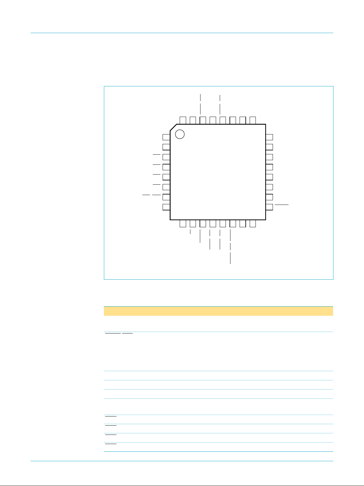
5.2 ISP1122ABD (LQFP32)
5.2.1 Pinning
dth
ISP1122A
USB stand-alone hub
DM3
32
DP3
1
V
2
CC
OC1
3
OC2
4
OC3
5
OC4
6
DM4
7
8
9
DP4
OC5/GOC
Fig 4. Pin configuration LQFP32.
GND
PSW2/GL2
31
30
ISP1122ABD
10
11
SP/BP
HUBGL
reg(3.3)
V
PSW1/GL1
29
28
12
13
PSW3/GL3
PSW4/GL4
DP2
DM2
DP0
27
26
25
14
15
16
MBL165
XTAL1
XTAL2
PSW5/GL5/GPSW
DM0
24
DP1
23
DM1
22
DP5
21
DM5
20
INDV/SDA
19
OPTION/SCL
18
RESET
17
5.2.2 Pin description
Table 3: Pin description for LQFP32
reg(3.3)
CC
[1]
[2]
Pin Type Description
29 - regulated supply voltage (3.3 V ± 10%) from internal
regulator; used to connect pull-up resistor on DP0 line
[3]
30 O modes 4 to 6: power switch control output for downstream
port 2 (open-drain, 6 mA)
modes 0 to 3, 7: GoodLink LED indicator output for
downstream port 2 (open-drain, 6 mA); to connect an LED
use a 330 Ω series resistor
[4]
[4]
2 - supply voltage; connect to USB supply V
hybrid-powered) or to local supply V
© Koninklijke Philips Electronics N.V. 2001. All rights reserved.
DD
(bus-poweredor
BUS
(self-powered)
[5]
)
[5]
)
[5]
)
[5]
)
Symbol
V
PSW2/GL2
GND 31 - ground supply
DM3 32 AI/O downstream port 3 D− connection (analog)
DP3 1 AI/O downstream port 3 D+ connection (analog)
V
OC1 3 AI/I overcurrent sense input for downstream port 1 (analog
OC2 4 AI/I overcurrent sense input for downstream port 2 (analog
OC3 5 AI/I overcurrent sense input for downstream port 3 (analog
OC4 6 AI/I overcurrent sense input for downstream port 4 (analog
9397 750 08958
Product data Rev. 03 — 30 October 2001 6 of 48
Page 7

Philips Semiconductors
ISP1122A
USB stand-alone hub
Table 3: Pin description for LQFP32
Symbol
OC5/GOC
[1]
Pin Type Description
[3]
7 AI/I modes 5, 7: overcurrent sense input for downstream port 5
(analog
modes 0, 1, 3: global overcurrent sense input (analog
DM4 8 AI/O downstream port 4 D− connection (analog)
DP4 9 AI/O downstream port 4 D+ connection (analog)
…continued
[5]
)
[5]
[4]
[4]
SP/BP 10 I selects power mode:
self-powered: connect to V
(local power supply); also use
DD
this mode for hybrid-powered operation
bus-powered:connect to GND; disable downstream port 5 to
meet supply current requirements
[4]
HUBGL 11 O hub GoodLink LED indicator output (open-drain, 6 mA);
to connect an LED use a 330 Ω series resistor; if unused
via a 10 kΩ resistor
CC
PSW3/GL3
connect to V
[3]
12 O modes 4 to 6: power switch control output for downstream
port 3 (open-drain, 6 mA)
modes 0 to 3, 7: GoodLink LED indicator output for
downstream port 3 (open-drain, 6 mA); to connect an LED
use a 330 Ω series resistor
PSW4/GL4
[3]
13 O modes 4 to 6: power switch control output for downstream
port 4 (open-drain, 6 mA)
modes 0 to 3, 7: GoodLink LED indicator output for
downstream port 4 (open-drain, 6 mA); to connect an LED
use a 330 Ω series resistor
PSW5/GL5/
[3]
GPSW
14 O mode 5: power switch control output for downstream port 5
(open-drain, 6 mA)
modes 3, 7: GoodLink LED indicator output for downstream
port 5 (open-drain, 6 mA); to connect an LED use a 330 Ω
series resistor
modes 0 to 2: gang mode power switch control output
(open-drain, 6 mA)
XTAL1 15 I crystal oscillator input (6 MHz)
XTAL2 16 O crystal oscillator output (6 MHz)
RESET
[2]
17 I reset input (Schmitt trigger); a LOW level produces an
asynchronous reset; connect to V
for power-on reset
CC
(internal POR circuit)
2
OPTION/SCL 18 I/O mode selection input; also functions as I
C-bus clock output
(open-drain, 6 mA)
INDV/SDA 19 I/O selects individual (HIGH) or global (LOW) power switching
and overcurrent detection; also functions as bidirectional
2
C-bus data line (open-drain, 6 mA)
I
DM5 20 AI/O downstream port 5 D− connection (analog)
DP5 21 AI/O downstream port 5 D+ connection (analog)
DM1 22 AI/O downstream port 1 D− connection (analog)
DP1 23 AI/O downstream port 1 D+ connection (analog)
[4]
[4]
[6]
[6]
DM0 24 AI/O upstream port D− connection (analog)
DP0 25 AI/O upstream port D+ connection (analog)
)
9397 750 08958
Product data Rev. 03 — 30 October 2001 7 of 48
© Koninklijke Philips Electronics N.V. 2001. All rights reserved.
Page 8

Philips Semiconductors
ISP1122A
USB stand-alone hub
Table 3: Pin description for LQFP32
Symbol
DM2 26 AI/O downstream port 2 D− connection (analog)
DP2 27 AI/O downstream port 2 D+ connection (analog)
PSW1/GL1
[1] Symbol names with an overscore (e.g. NAME) indicate active LOW signals.
[2] The voltage at pin V
[3] See Table 4 “Mode selection”.
[4] To disable a downstream port connect both D+ and D− to VCCvia a 1 MΩ resistor; unused ports must
[5] Analog detection circuit can be switched off using an external EEPROM, see Table 23; in this case,
[6] Downstream ports 1 and 2 cannot be disabled.
[1]
connecting RESET to V
be disabled in reverse order starting from port 5.
the pin functions as a logic input (TTL level).
6. Functional description
The ISP1122A is a stand-alone USB hub with up to 5 downstream ports. The number
of ports can be configured between 2 and 5. The downstream ports can be used to
connect low-speed or full-speed USB peripherals. All standard USB requests from
the host are handled by the hardware without the need for firmware intervention. The
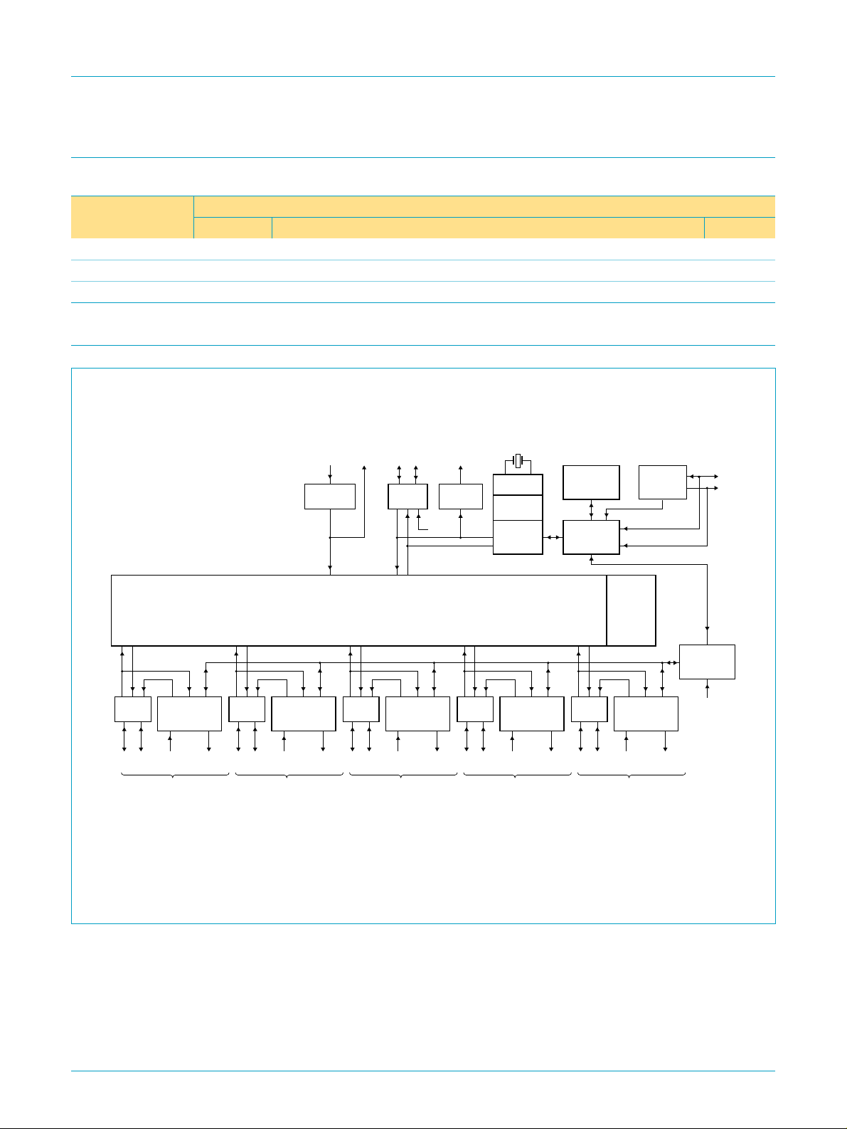
block diagram is shown in Figure 1.
…continued
Pin Type Description
[6]
[6]
[3]
28 O modes 4 to 6: power switch control output for downstream
port 1 (open-drain, 6 mA)
modes 0 to 3, 7: GoodLink LED indicator output for
downstream port 1 (open-drain, 6 mA); to connect an LED
use a 330 Ω series resistor
is gated by the RESET pin. This allows fully self-powered operation by
reg(3.3)
(+5 V USB supply). If V
BUS
is lost upstream port D+ will not be driven.
BUS
The ISP1122A requires only a single supply voltage. An internal 3.3 V regulator
provides the supply voltage for the analog USB data transceivers.
The ISP1122A supports both bus-powered and self-powered hub operation. When
using bus-powered operation a downstream port cannot supply more than 100 mA to
a peripheral. In case of self-powered operation an external supply is used to power
the downstream ports, allowing a current consumption of max. 500 mA per port.
A basic I2C-bus interface is provided for reading vendor ID, product ID and
configuration bits from an external EEPROM upon a reset.
6.1 Analog transceivers
The integrated transceiver interfaces directly to the USB cables through external
termination resistors. They are capable of transmitting and receiving serial data at
both ‘full-speed’ (12 Mbit/s) and ‘low-speed’ (1.5 Mbit/s) data rates. The slew rates
are adjusted according to the speed of the device connected and lie within the range
mentioned in the
USB Specification Rev. 1.1
.
9397 750 08958
Product data Rev. 03 — 30 October 2001 8 of 48
© Koninklijke Philips Electronics N.V. 2001. All rights reserved.
Page 9

Philips Semiconductors
6.2 Philips Serial Interface Engine (SIE)
The Philips SIE implements the full USB protocol layer. It is completely hardwired for
speed and needs no firmware intervention. The functions of this block include:
synchronization pattern recognition, parallel/serial conversion, bit (de-)stuffing, CRC
checking/generation, Packet IDentifier (PID) verification/generation, address
recognition, handshake evaluation/generation.
6.3 Hub repeater
The hub repeater is responsible for managing connectivity on a ‘per packet’ basis. It
implements ‘packet signalling’ and ‘resume’ connectivity. Low-speed devices can be
connected to downstream ports. If a low-speed device is detected the repeater will
not propagate upstream packets to the corresponding port, unless they are preceded
by a PREAMBLE PID.
6.4 End-of-frame timers
This block contains the specified EOF1 and EOF2 timers which are used to detect
‘loss-of-activity’ and ‘babble’ error conditions in the hub repeater. The timers also
maintain the low-speed keep-alive strobe which is sent at the beginning of a frame.
ISP1122A
USB stand-alone hub
6.5 General and individual port controller
The general and individual port controllers together provide status and control of
individual downstream ports. Any port status change will be reported to the host via
the hub status change (interrupt) endpoint.
6.6 GoodLink
Indication of a good USB connection is provided through GoodLink technology. An
LED can be directly connected via an external 330 Ω resistor.
During enumeration the LED blinks on momentarily. After successful configuration of
the ISP1122A, the LED is permanently on. The LED blinks off for 100 ms upon each
successful packet transfer (with ACK). The hub GoodLink indicator blinks when the
hub receives a packet addressed to it. Downstream GoodLink indicators blink upon
an acknowledgment from the associated port. In ‘suspend’ mode the LED is off.
This feature provides a user-friendly indication of the status of the hub, the connected
downstream devices and the USB traffic. It is a useful diagnostics tool to isolate faulty
USB equipment and helps to reduce field support and hotline costs.
6.7 Bit clock recovery
The bit clock recovery circuit recovers the clock from the incoming USB data stream
using a 4× oversampling principle. It is able to track jitter and frequency drift as
specified by the
USB Specification Rev. 1.1
.
6.8 Voltage regulator
A 5 to 3.3 V DC-DC regulator is integrated on-chip to supply the analog transceiver
and internal logic. This can also be used to supply the terminal 1.5 kΩ pull-up resistor
on the D+ line of the upstream connection.
9397 750 08958
Product data Rev. 03 — 30 October 2001 9 of 48
© Koninklijke Philips Electronics N.V. 2001. All rights reserved.
Page 10

Philips Semiconductors
6.9 PLL clock multiplier
A 6 to 48 MHz clock multiplier Phase-Locked Loop (PLL) is integrated on-chip. This
allows for the use of low-cost 6 MHz crystals. The low crystal frequency also
minimizes Electro-Magnetic Interference (EMI). The PLL requires no external
components.
6.10 Overcurrent detection
An overcurrent detection circuit for downstream ports has been integrated on-chip. It
is self-reporting, resets automatically, has a low trip time and requires no external
components. Both individual and global overcurrent detection are supported.
6.11 I2C-bus interface
A basic serial I2C-bus interface (single master, 100 kHz) is provided to read VID, PID
and configuration bits from an external I2C-bus EEPROM (e.g. Philips PCF8582 or
equivalent). At reset the ISP1122A reads 6 bytes of data from the external memory.
The I2C-bus interface timing complies with the standard mode of operation as
described in
The I2C-bus and how to use it
ISP1122A
USB stand-alone hub
, order number 9398 393 40011.
7. Modes of operation
The ISP1122A has several modes of operation, each corresponding with a different
pin configuration. Modes are selected by means of pins INDV, OPTION and SP/BP,
as shown in Table 4.
Table 4: Mode selection
Mode INDV
0000GoodLink ganged power inactive global overcurrent
1001GoodLink ganged power inactive global overcurrent
2010GoodLink ganged power inactive
3011GoodLink
4100individual power inactive individual
5101individual power individual power individual
6110individual power inactive inactive
7111GoodLink
[1] Port power switching: logic 0 = ganged, logic 1 = individual.
[2] Power mode: logic 0 = bus-powered, logic 1 = self-powered (or hybrid-powered).
[3] No overcurrent detection.
[4] No power switching.
[1]
OPTION SP/BP
[2]
PSWn/GLn
(n = 1 to 4)
PSW5/GL5/GPSW OCn
[4]
[4]
GoodLink
GoodLink
[4]
[4]
(n = 1 to 4)
[3]
inactive global overcurrent
overcurrent
overcurrent
[3]
individual
overcurrent
OC5/GOC
inactive
inactive
individual
overcurrent
inactive
individual
overcurrent
[3]
[3]
9397 750 08958
Product data Rev. 03 — 30 October 2001 10 of 48
© Koninklijke Philips Electronics N.V. 2001. All rights reserved.
Page 11

Philips Semiconductors
8. Endpoint descriptions
Each USB device is logically composed of several independent endpoints. An
endpoint acts as a terminus of a communication flow between the host and the
device. At design time each endpoint is assigned a unique number (endpoint
identifier, see Table 5). The combination of the device address (given by the host
during enumeration), the endpoint number and the transfer direction allows each
endpoint to be uniquely referenced.
The ISP1122A has two endpoints, endpoint 0 (control) and endpoint 1 (interrupt).
Table 5: Hub endpoints
Function Ports Endpoint
Hub
[1] IN: input for the USB host; OUT: output from the USB host.
0: upstream
1 to 5: downstream
ISP1122A
USB stand-alone hub
identifier
0 control
1 interrupt IN 1
Transfer
type
Direction
OUT 64
IN 64
[1]
Max. packet
size (bytes)
8.1 Hub endpoint 0 (control)
All USB devices and functions must implement a default control endpoint (ID = 0).
This endpoint is used by the host to configure the device and to perform generic USB
status and control access.
The ISP1122A hub supports the following USB descriptor information through its
control endpoint 0, which can handle transfers of 64 bytes maximum:
Device descriptor
•
Configuration descriptor
•
Interface descriptor
•
Endpoint descriptor
•
Hub descriptor
•
String descriptor.
•
8.2 Hub endpoint 1 (interrupt)
Endpoint 1 is used by the ISP1122A hub to provide status change information to the
host. This endpoint can be accessed only after the hub has been configured by the
host (by sending the Set Configuration command).
Endpoint 1 is an interrupt endpoint: the host polls it once every 255 ms by sending an
IN token. If the hub has detected no change in the port status it returns a NAK (Not
AcKnowledge) response to this request, otherwise it sends the Status Change byte
(see Table 6).
9397 750 08958
Product data Rev. 03 — 30 October 2001 11 of 48
© Koninklijke Philips Electronics N.V. 2001. All rights reserved.
Page 12

Philips Semiconductors
Table 6: Status Change byte: bit allocation
Bit Symbol Description
0 Hub SC a logic 1 indicates a status change on the hub’s upstream port
1 Port 1 SC a logic 1 indicates a status change on downstream port 1
2 Port 2 SC a logic 1 indicates a status change on downstream port 2
3 Port 3 SC a logic 1 indicates a status change on downstream port 3
4 Port 4 SC a logic 1 indicates a status change on downstream port 4
5 Port 5 SC a logic 1 indicates a status change on downstream port 5
6 reserved not used
7 reserved not used
9. Host requests
The ISP1122A handles all standard USB requests from the host via control
endpoint 0. The control endpoint can handle a maximum of 64 bytes per transfer.
Remark: Please note that the USB data transmission order is Least Significant Bit
(LSB) first. In the following tables multi-byte variables are displayed least significant
byte first.
ISP1122A
USB stand-alone hub
9.1 Standard requests
Table 7 shows the supported standard USB requests. Some requests are explicitly
unsupported. All other requests will be responded to with a STALL packet.
Table 7: Standard USB requests
Request name bmRequestType
Address
Set Address X000 0000 05 address
Configuration
Get Configuration 1000 0000 08 00, 00 00, 00 01, 00 configuration
Set Configuration (0) X000 0000 09 00, 00 00, 00 00, 00 none
Set Configuration (1) X000 0000 09 01, 00 00, 00 00, 00 none
Descriptor
Get Configuration
Descriptor
Get Device Descriptor 1000 0000 06 00, 01 00, 00 length
Get String Descriptor (0) 1000 0000 06 03, 00 00, 00 length
Get String Descriptor (1) 1000 0000 06 03, 01 00, 00 length
Get String Descriptor (2) 1000 0000 06 03, 02 00, 00 length
byte 0 [7:0]
(Bin)
1000 0000 06 00, 02 00, 00 length
bRequest
byte 1
(Hex)
wValue
byte 2, 3
(Hex)
wIndex
byte 4, 5
(Hex)
[1]
00, 00 00, 00 none
wLength
byte 6, 7
(Hex)
Data
value = 01H
[2]
[2]
[2]
[2]
[2]
configuration,
interface and
endpoint
descriptors
device
descriptor
language ID
string
manufacturer
string
product string
9397 750 08958
Product data Rev. 03 — 30 October 2001 12 of 48
© Koninklijke Philips Electronics N.V. 2001. All rights reserved.
Page 13

Philips Semiconductors
ISP1122A
USB stand-alone hub
Table 7: Standard USB requests
Request name bmRequestType
byte 0 [7:0]
(Bin)
…continued
bRequest
byte 1
(Hex)
wValue
byte 2, 3
(Hex)
wIndex
byte 4, 5
(Hex)
wLength
byte 6, 7
(Hex)
Data
Feature
Clear Device Feature
X000 0000 01 01, 00 00, 00 00, 00 none
(REMOTE_WAKEUP)
Clear Endpoint (1)
X000 0010 01 00, 00 81, 00 00, 00 none
Feature (HALT/STALL)
Set Device Feature
X000 0000 03 01, 00 00, 00 00, 00 none
(REMOTE_WAKEUP)
Set Endpoint (1)
X000 0010 03 00, 00 81, 00 00, 00 none
Feature (HALT/STALL)
Status
Get Device Status 1000 0000 00 00, 00 00, 00 02, 00 device status
Get Interface Status 1000 0001 00 00, 00 00, 00 02, 00 zero
[3]
Get Endpoint (0) Status 1000 0010 00 00, 00 00/80
, 00 02, 00 endpoint 0
status
Get Endpoint (1) Status 1000 0010 00 00, 00 81, 00 02, 00 endpoint 1
status
Unsupported
Set Descriptor 0000 0000 07 XX, XX XX, XX XX, XX descriptor;
STALL
Get Interface 1000 0001 0A 00, 00 XX, XX 01, 00 STALL
Set Interface X000 0001 0B XX, XX XX, XX 00, 00 STALL
Synch Frame 1000 0010 0C 00, 00 XX, XX 02, 00 STALL
[1] Device address: 0 to 127.
[2] Returned value in bytes.
[3] MSB specifies endpoint direction: 0 = OUT, 1 = IN. The ISP1122A accepts either value.
9.2 Hub specific requests
In Table 8 the supported hub specific requests are listed, as well as some
unsupported requests. Table 9 provides the feature selectors for setting or clearing
port features.
Table 8: Hub specific requests
Request name bmRequestType
byte 0 [7:0]
(Bin)
Descriptor
Get Hub Descriptor 1010 0000 06 00, 00/29
Feature
Clear Hub Feature
X010 0000 01 00, 00 00, 00 00, 00 none
(C_LOCAL_POWER)
Clear Port Feature
X010 0011 01 feature
(feature selectors)
Set Port Feature
X010 0011 03 feature
(feature selectors)
bRequest
byte 1
(Hex)
wValue
byte 2, 3
(Hex)
[1]
[3]
, 00 port
[3]
, 00 port
wIndex
byte 4, 5
(Hex)
00, 00 length
wLength
byte 6, 7
(Hex)
[2]
, 00 hub descriptor
[4]
, 00 00, 00 none
[4]
, 00 00, 00 none
Data
9397 750 08958
Product data Rev. 03 — 30 October 2001 13 of 48
© Koninklijke Philips Electronics N.V. 2001. All rights reserved.
Page 14

Philips Semiconductors
ISP1122A
USB stand-alone hub
Table 8: Hub specific requests
Request name bmRequestType
…continued
byte 0 [7:0]
(Bin)
bRequest
byte 1
(Hex)
wValue
byte 2, 3
(Hex)
wIndex
byte 4, 5
(Hex)
wLength
byte 6, 7
(Hex)
Data
Status
Get Hub Status 1010 0000 00 00, 00 00, 00 04, 00 hubstatus and
status change
field
[4]
Get Port Status 1010 0011 00 00, 00 port
, 00 04, 00 port status
Unsupported
[4]
Get Bus Status 1010 0011 02 00, 00 port
Clear Hub Feature
X010 0000 01 01, 00 00, 00 00, 00 STALL
, 00 01, 00 STALL
(C_OVER_CURRENT)
Set Hub Descriptor 0010 0000 07 XX, XX 00, 00 3E, 00 STALL
Set Hub Feature
X010 0000 03 00, 00 00, 00 00, 00 STALL
(C_LOCAL_POWER)
Set Hub Feature
X010 0000 03 01, 00 00, 00 00, 00 STALL
(C_OVER_CURRENT)
[1]
USB Specification Rev. 1.0
[2] Returned value in bytes.
[3] Feature selector value, see Table 9.
[4] Downstream port identifier: 1 to N with N = number of enabled ports (2 to 5).
uses 00H,
USB Specification Rev. 1.1
specifies 29H.
Table 9: Port feature selectors
Feature selector name Value (Hex) Set feature Clear feature
PORT_CONNECTION 00 not used not used
PORT_ENABLE 01 not used disables a port
PORT_SUSPEND 02 suspends a port resumes a port
PORT_OVERCURRENT 03 not used not used
PORT_RESET 04 resets and enables a
not used
port
PORT_POWER 08 powers on a port powers off a port
PORT_LOW_SPEED 09 not used not used
C_PORT_CONNECTION 10 not used clears port connection
change bit
C_PORT_ENABLE 11 not used clears port enable
change bit
C_PORT_SUSPEND 12 not used clears port suspend
change bit
C_PORT_OVERCURRENT 13 not used clears port overcurrent
change bit
C_PORT_RESET 14 not used clears port reset
change bit
9397 750 08958
Product data Rev. 03 — 30 October 2001 14 of 48
© Koninklijke Philips Electronics N.V. 2001. All rights reserved.
Page 15

Philips Semiconductors
9.3 Descriptors
The ISP1122A hub controller supports the following standard USB descriptors:
•
•
•
•
•
•
Table 10: Device descriptor
Values in square brackets are optional.
Offset
(bytes)
0 bLength 1 12 descriptor length = 18 bytes
1 bDescriptorType 1 01 type = DEVICE
2 bcdUSB 2 10, 01
4 bDeviceClass 1 09 HUB_CLASSCODE
5 bDeviceSubClass 1 00 6 bDeviceProtocol 1 00 7 bMaxPacketSize0 1 40 packet size = 64 bytes
8 idVendor 2 CC, 04 Philips Semiconductors vendor ID
10 idProduct 2 22, 11 ISP1122A product ID; can be
12 bcdDevice 2 01, 01 device release 1.1; silicon revision
14 iManufacturer 1 00 no manufacturer string (default)
15 iProduct 1 00 no product string (default)
16 iSerialNumber 1 00 no serial number string
17 bNumConfigurations 1 01 one configuration
Device
Configuration
Interface
Endpoint
Hub
String.
Field name Size
(bytes)
ISP1122A
USB stand-alone hub
Value
(Hex)
[01] manufacturer string enabled
[02] product string enabled
Comments
USB Specification Rev. 1.1
(04CC); can be customized using an
external EEPROM (see Table 23)
customized using an external
EEPROM (see Table 23)
increments this value
(using an external EEPROM)
(using an external EEPROM)
9397 750 08958
Product data Rev. 03 — 30 October 2001 15 of 48
© Koninklijke Philips Electronics N.V. 2001. All rights reserved.
Page 16

Philips Semiconductors
Table 11: Configuration descriptor
Values in square brackets are optional.
Offset
(bytes)
0 bLength 1 09 descriptor length=9bytes
1 bDescriptorType 1 02 type = CONFIGURATION
2 wTotalLength 2 19, 00 total length of configuration, interface
4 bNumInterfaces 1 01 one interface
5 bConfigurationValue 1 01 configuration value = 1
6 iConfiguration 1 00 no configuration string
7 bmAttributes 1 E0 self-powered with remote wake-up
8 MaxPower
[1] Selected by input SP/BP.
[2] Value in units of 2 mA.
Field name Size
(bytes)
[2]
1 32 100 mA (default)
ISP1122A
USB stand-alone hub
Value
(Hex)
A0 bus-powered with remote wake-up
[00] 0 mA (using an external EEPROM)
[FA] 500 mA (using an external EEPROM)
Comments
and endpoint descriptors (25 bytes)
[1]
[1]
Table 12: Interface descriptor
Offset
(bytes)
Field name Size
(bytes)
Value
(Hex)
Comments
0 bLength 1 09 descriptor length=9bytes
1 bDescriptorType 1 04 type = INTERFACE
2 bInterfaceNumber 1 00 3 bAlternateSetting 1 01 no alternate setting
4 bNumEndpoints 1 01 status change (interrupt) endpoint
5 bInterfaceClass 1 09 HUB_CLASSCODE
6 bInterfaceSubClass 1 00 7 bInterfaceProtocol 1 00 no class-specific protocol
8 bInterface 1 00 no interface string
Table 13: Endpoint descriptor
Offset
(bytes)
Field name Size
(bytes)
Value
(Hex)
Comments
0 bLength 1 07 descriptor length=7bytes
1 bDescriptorType 1 05 type = ENDPOINT
2 bEndpointAddress 1 81 endpoint 1, direction: IN
3 bmAttributes 1 03 interrupt endpoint
4 wMaxPacketSize 2 01, 00 packet size = 1 byte
6 bInterval 1 FF polling interval (255 ms)
9397 750 08958
Product data Rev. 03 — 30 October 2001 16 of 48
© Koninklijke Philips Electronics N.V. 2001. All rights reserved.
Page 17

Philips Semiconductors
Table 14: Hub descriptor
Values in square brackets are optional.
Offset
(bytes)
0 bDescLength 1 09 descriptor length=9bytes
1 bDescriptorType 1 29 type = HUB
2 bNbrPorts 1 05 to 02 number of enabled downstream ports;
3 wHubCharacteristics 2 09, 00 individual power switching
5 bPwrOn2PwrGood
6 bHubContrCurrent 1 64 maximum hub controller current
7 DeviceRemovable 1 00 all devices removable
8 PortPwrCtrlMask 1 FF must be all ones for compatibility with
Field name Size
(bytes)
[3]
1 32 100 ms (default; modes 0, 1, 2, 4, 5, 6)
ISP1122A
USB stand-alone hub
Value
(Hex)
11, 00 individual power switching
00 0 ms (default; modes 3, 7)
[FA] 500 ms (using an external EEPROM;
Comments
selectable by DP/DM strapping
[1]
,
overcurrent protection active
(modes 0, 1, 3, 4, 5, 7)
[1]
, no
overcurrent protection (modes 2, 6)
modes 0, 1, 2, 4, 5, 6); see Table 23
(100 mA)
USB Specification Rev. 1.0
[2]
[1] ISP1122A always reports power management status on an individual basis, even for ganged/global
modes. This is compliant with
[2] Condition with no overcurrent detection is reported to the host.
[3] Value in units of 2 ms.
USB Specification Rev. 1.1
.
Table 15: String descriptors
String descriptors are optional and therefore disabled by default; they can be enabled through
an external EEPROM.
Offset
(bytes)
Field name Size
(bytes)
Value
(Hex)
Comments
String descriptor (0): language ID string
0 bLength 1 04 descriptor length=4bytes
1 bDescriptorType 1 03 type = STRING
2 bString 2 09, 04 LANGID code zero
String descriptor (1): manufacturer string
0 bLength 1 2E descriptor length = 46 bytes
1 bDescriptorType 1 03 type = STRING
[1]
2 bString 44 UC
“Philips Semiconductors”
String descriptor (2): product string
0 bLength 1 10 descriptor length = 16 bytes
1 bDescriptorType 1 03 type = STRING
[1]
2 bString 14 UC
“ISP1122”
[1] Unicode encoded string.
9397 750 08958
Product data Rev. 03 — 30 October 2001 17 of 48
© Koninklijke Philips Electronics N.V. 2001. All rights reserved.
Page 18

Philips Semiconductors
9.4 Hub responses
This section describes the hub responses to requests from the USB host.
9.4.1 Get device status
The hub returns 2 bytes, see Table 16.
Table 16: Get device status response
Bit # Function Value Description
0 self-powered 0 bus-powered
1 remote wake-up 0 no remote wake-up
2 to 15 reserved 0 -
9.4.2 Get configuration
The hub returns 1 byte, see Table 17.
Table 17: Get configuration response
Bit # Function Value Description
0 configuration value 0 device not configured
1 to 7 reserved 0 -
ISP1122A
USB stand-alone hub
1 self-powered
1 remote wake-up enabled
1 device configured
9.4.3 Get interface status
The hub returns 2 bytes, see Table 18.
Table 18: Get interface status response
Bit # Function Value Description
0 to 15 reserved 0 -
9.4.4 Get hub status
The hub returns 4 bytes, see Table 19.
Table 19: Get hub status response
Bit # Function Value Description
0 local power source 0 local power supply good
1 overcurrent indicator 0 no overcurrent condition
2 to 15 reserved 0 16 local power status change 0 no change in local power status
17 overcurrent indicator change 0 no change in overcurrent condition
18 to 31 reserved 0 -
1 local power supply lost
1 hub overcurrent condition detected
1 local power status changed
1 overcurrent condition changed
9397 750 08958
Product data Rev. 03 — 30 October 2001 18 of 48
© Koninklijke Philips Electronics N.V. 2001. All rights reserved.
Page 19

Philips Semiconductors
9.4.5 Get port status
The hub returns 4 bytes. The first 2 bytes contain the port status bits (wPortStatus,
see Table 20). The last 2 bytes hold the port status change bits (wPortChange, see
Table 21).
Table 20: Get port status response (wPortStatus)
Bit # Function Value Description
0 current connect status 0 no device present
1 port enabled/disabled 0 port disabled
2 suspend 0 port not suspended
3 overcurrent indicator 0 no overcurrent condition
4 reset 0 reset not asserted
5 to 7 reserved 0 8 port power 0 port powered off
9 low-speed device attached 0 full-speed device attached
10 to 15 reserved 0 -
ISP1122A
USB stand-alone hub
1 device present on this port
1 port enabled
1 port suspended
1 overcurrent condition detected
1 reset asserted
1 port power on
1 low-speed device attached
Table 21: Get port status response (wPortChange)
Bit # Function Value Description
0 connect status change 0 no change in current connect status
1 current connect status changed
1 port enabled/disabled
change
2 suspend change 0 no change in suspend status
3 overcurrent indicator change 0 no change in overcurrent status
4 reset change 0 no change in reset status
5 to 15 reserved 0 -
0 no port error
1 port disabled by a port error
1 resume complete
1 overcurrent indicator changed
1 reset complete
9397 750 08958
Product data Rev. 03 — 30 October 2001 19 of 48
© Koninklijke Philips Electronics N.V. 2001. All rights reserved.
Page 20

Philips Semiconductors
9.4.6 Get configuration descriptor
The hub returns 25 bytes containing the configuration descriptor (9 bytes, see
Table 11), the interface descriptor (9 bytes, see Table 12) and the endpoint descriptor
(7 bytes, see Table 13).
9.4.7 Get device descriptor
The hub returns 18 bytes containing the device descriptor, see Table 10.
9.4.8 Get hub descriptor
The hub returns 9 bytes containing the hub descriptor, see Table 14.
9.4.9 Get string descriptor (0)
The hub returns 4 bytes containing the language ID, see Table 15.
9.4.10 Get string descriptor (1)
The hub returns 46 bytes containing the manufacturer name, see Table 15.
9.4.11 Get string descriptor (2)
The hub returns 16 bytes containing the product name, see Table 15.
ISP1122A
USB stand-alone hub
10. I2C-bus interface
A simple I2C-bus interface is provided in the ISP1122A to read customized vendor ID,
product ID and some other configuration bits from an external EEPROM. The
interface supports single master operation at a nominal bus speed of 93.75 kHz.
The I2C-bus interface is intended for bidirectional communication between ICs via two
serial bus wires, SDA (data) and SCL (clock). Both lines are driven by open-drain
circuits and must be connected to the positive supply voltage via pull-up resistors.
10.1 Protocol
The I2C-bus protocol defines the following conditions:
•
•
•
•
Each device on the I2C-bus has a unique slave address, which the master uses to
select a device for access.
The master starts a data transfer using a START condition and ends it by generating
a STOP condition. Transfers can only be initiated when the bus is free. The receiver
must acknowledge each byte by means of a LOW level on SDA during the ninth clock
pulse on SCL.
Bus free: both SDA and SCL are HIGH
START: a HIGH-to-LOW transition on SDA, while SCL is HIGH
STOP: a LOW-to-HIGH transition on SDA, while SCL is HIGH
Data valid: after a START condition, data on SDA are stable during the HIGH
period of SCL; data on SDA may only change while SCL is LOW.
For detailed information please consult
9398 393 40011.
9397 750 08958
Product data Rev. 03 — 30 October 2001 20 of 48
The I2C-bus and how to use it
© Koninklijke Philips Electronics N.V. 2001. All rights reserved.
., order number
Page 21
Philips Semiconductors
10.2 Hardware connections
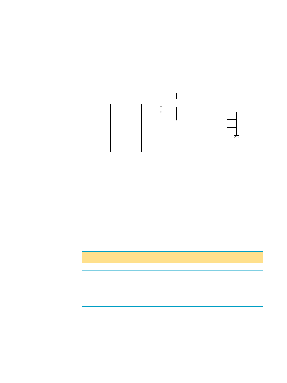
Via the I2C-bus interface the ISP1122A can be connected to an external EEPROM
(PCF8582 or equivalent). The hardware connections are shown in Figure 5.
The SCL and SDA pins are multiplexed with pins OPTION and INDV respectively.
ISP1122A
USB stand-alone hub
dth
Fig 5. EEPROM connection diagram.
The slaveaddress which ISP1122A uses to access the EEPROM is 1010000B. Page
mode addressing is not supported, so pins A0, A1 and A2 of the EEPROM must be
connected to GND (logic 0).
10.3 Data transfer
When the ISP1122A is reset, the I2C-bus interface tries to read 6 bytes of
configuration data from an external EEPROM. If no response is detected, the levels
on inputs SDA and SCL are interpreted as INDV and OPTION to select the operating
mode (see Table 4).
OPTION/SCL
INDV/SDA
ISP1122A
USB HUB
V
DD
R
2
I
P
C-bus
V
DD
R
P
SCL
SDA
PCF8582
EEPROM
equivalent
A0
A1
A2
or
MBL166
The data in the EEPROM memory are organized as shown in Table 22.
Table 22: EEPROM organization
Address
(Hex)
00 CC idVendor
01 04 idVendor
02 22 idProduct
03 11 idProduct
04 - configuration bits C7 to C0; see Table 23
05 AA signature
[1] Vendor ID code in the Device descriptor, seeTable 10.
[2] Product ID code in the Device descriptor, see Table 10.
9397 750 08958
Product data Rev. 03 — 30 October 2001 21 of 48
Default value
(Hex)
Contents
[1]
(lower byte)
[1]
(upper byte)
[2]
(lower byte)
[2]
(upper byte)
© Koninklijke Philips Electronics N.V. 2001. All rights reserved.
Page 22

Philips Semiconductors
Table 23: Configuration bits
Bit Function Value
C0 OPTION see Table 4 “Mode selection”
C1 INDV see Table 4 “Mode selection”
C2 reserved 0
C3 PwrOn2PwrGood
C4 string descriptor enable 0
C5 internal analog overcurrent
C7, C6 MaxPower
detection enable
[3]
ISP1122A
USB stand-alone hub
(Bin)
[1]
[2]
[1]
0
1 500 ms (bPwrOn2PwrGood = FAH)
[1]
1 string descriptors enabled (strings:
0 internal analog overcurrent detection
[1]
1
[1]
00
1X 500 mA (MaxPower= FAH)
01 0 mA (MaxPower= 00H)
Description
must always be programmed to logic 0
100 ms (bPwrOn2PwrGood = 32H)
string descriptors disabled
“Philips Semiconductors”, “ISP1122”)
circuit disabled; overcurrent pins
function as digital inputs (TTL level)
internal analog overcurrent detection
circuit enabled
100 mA (MaxPower= 32H)
OCn
[1] Default value at reset if no external EEPROM is present.
[2] Modifies the Hub Descriptor field ‘bPwrOn2PwrGood’, see Table 14.
[3] Modifies the Hub Descriptor field ‘MaxPower’, seeTable 14.
11. Hub power modes
USB hubs can either be self-powered or bus-powered.
Self-powered — Self-powered hubs have a 5 V local power supply on board which
provide power to the hub and the downstream ports. The
requires that these hubs limit the current to 500 mA per downstream port and report
overcurrent conditions to the host. The hub may optionally draw 100 mA from the
USB supply (V
Bus-powered — Bus-powered hubs obtain all power from the host or an upstream
self-powered hub. The maximum current is 100 mA per downstream port. Current
limiting and reporting of overcurrent conditions are both optional.
Power switching of downstream ports can be done individually or ganged, where all
ports are switched simultaneously with one power switch. The ISP1122A supports
both modes, which can be selected using input INDV (see Table 4).
11.1 Voltage drop requirements
USB Specification Rev. 1.1
) to power the interface functions (hybrid-powered).
BUS
11.1.1 Self-powered hubs
Self-powered hubs are required to provide a minimum of 4.75 V to its output port
connectors at all legal load conditions. To comply with Underwriters Laboratory Inc.
(UL) safety requirements, the power from any port must be limited to 25 W (5 A at
5 V). Overcurrent protection may be implemented on a global or individual basis.
9397 750 08958
Product data Rev. 03 — 30 October 2001 22 of 48
© Koninklijke Philips Electronics N.V. 2001. All rights reserved.
Page 23
Philips Semiconductors
Assuming a 5 V ± 3% power supply the worst case supply voltage is 4.85 V. This only
allows a voltage drop of 100 mV across the hub printed-circuit board (PCB) to each
downstream connector. This includes a voltage drop across:
•
•
•
•
PCB resistance and power supply connector resistance may cause a drop of 25 mV,
leaving only 75 mV as the voltage drop allowed across the power switch and
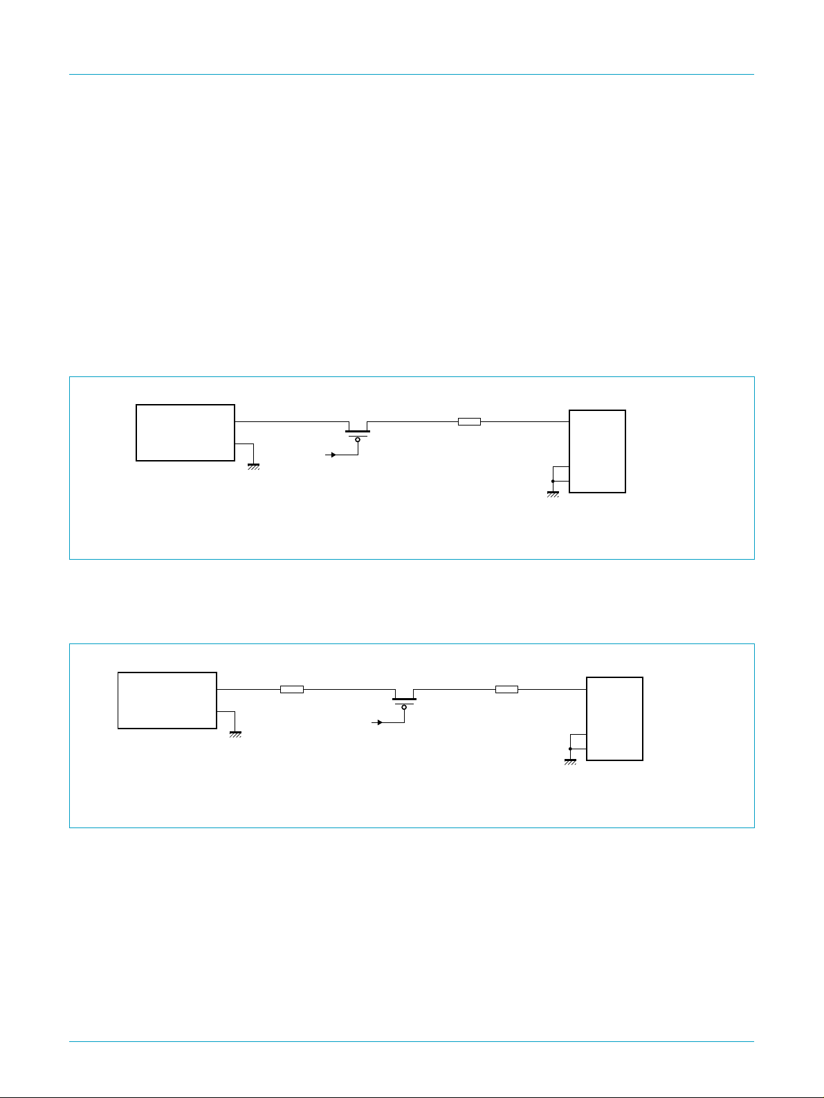
overcurrent sense device. The individual voltage drop components are shown in
Figure 6.
ISP1122A
USB stand-alone hub
Power supply connector
Hub PCB (power and ground traces, ferrite beads)
Power switch (FET on-resistance)
Overcurrent sense device.
voltage drop
25 mV
hub board
resistance
4.75 V(min)
(1)
V
BUS
D+
D−
GND
SHIELD
04aa03
downstream
port
connector
5 V
POWER SUPPLY
± 3% regulated
(1) Includes PCB traces, ferrite beads, etc.
+
−
4.85 V(min)
voltage drop
ISP1122A
power
switch
75 mV
low-ohmic
PMOS switch
Fig 6. Typical voltage drop components in self-powered mode using individual overcurrent detection.
In case of global overcurrent detection an increased voltage drop is needed for the
overcurrent sense device (in this case a low-ohmic resistor). This can be realized by
using a special power supply of 5.1 V ± 3%, as shown in Figure 7.
voltage drop
5.1 V KICK-UP
POWER SUPPLY
± 3% regulated
(1) Includes PCB traces, ferrite beads, etc.
4.95 V(min)
+
−
100 mV
low-ohmic
sense resistor
for overcurrent
detection
voltage drop
ISP1122A
power
switch
75 mV
low-ohmic
PMOS switch
Fig 7. Typical voltage drop components in self-powered mode using global overcurrent detection.
voltage drop
25 mV
hub board
resistance
4.75 V(min)
(1)
V
BUS
D+
D−
GND
SHIELD
04aa05
downstream
port
connector
11.1.2 Bus-powered hubs
Bus-powered hubs are guaranteed to receive a supply voltage of 4.5 V at the
upstream port connector and must provide a minimum of 4.4 V to the downstream
port connectors. The voltage drop of 100 mV across bus-powered hubs includes:
Hub PCB (power and ground traces, ferrite beads)
•
Power switch (FET on-resistance)
•
Overcurrent sense device.
•
9397 750 08958
Product data Rev. 03 — 30 October 2001 23 of 48
© Koninklijke Philips Electronics N.V. 2001. All rights reserved.
Page 24
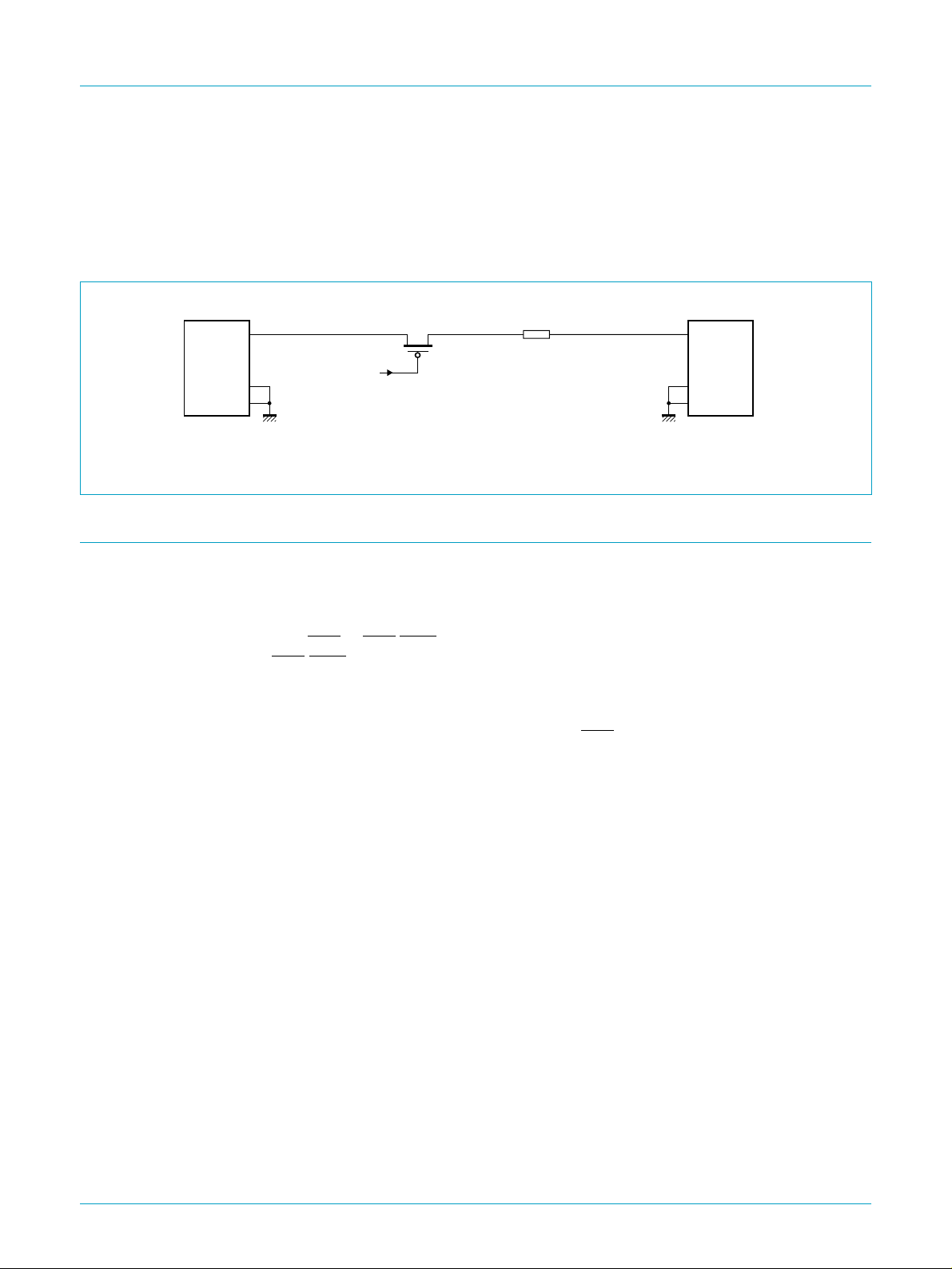
Philips Semiconductors
The PCB resistance may cause a drop of 25 mV, which leaves 75 mV for the power
switch and overcurrent sense device. The voltage drop components are shown in
Figure 8.
For bus-powered hubs overcurrent protection is optional. It may be implemented for
all downstream ports on a global or individual basis.
ISP1122A
USB stand-alone hub
voltage drop
25 mV
hub board
resistance
4.40 V(min)4.50 V(min)
(1)
V
BUS
upstream
port
connector
(1) Includes PCB traces, ferrite beads, etc.
D+
D−
GND
SHIELD
voltage drop
ISP1122A
power
switch
75 mV
low-ohmic
PMOS switch
Fig 8. Typical voltage drop components in bus-powered mode (no overcurrent detection).
12. Overcurrent detection
The ISP1122A has an analog overcurrent detection circuit for monitoring downstream
port lines. This circuit automatically reports an overcurrent condition to the host and
turns off the power to the faulty port. The host must reset the condition flag.
Pins OC1 to OC5/GOC are used for individual port overcurrent detection. Pin
OC5/GOC can also be used for global overcurrent detection. This is controlled by
input INDV (see Table 4).
The overcurrent detection circuit can be switched off using an external EEPROM (see
Table 23). In this case, the overcurrent pins OCn function as logic inputs (TTL level).
V
BUS
D+
D−
GND
SHIELD
04aa06
downstream
port
connector
12.1 Overcurrent circuit description
The integrated overcurrent detection circuit of ISP1122A senses the voltage drop
across the power switch or an extra low-ohmic sense resistor. When the port draws
too much current, the voltage drop across the power switch exceeds the trip voltage
threshold (∆V
switch control signal after a delay of 15 ms (t
). The overcurrent circuit detects this and switches off the power
trip
). This delay acts as a ‘debounce’
trip
period to minimize false tripping, especially during the inrush current produced by ‘hot
plugging’ of a USB device.
12.2 Power switch selection
From the voltage drop analysis given in Figure 6, Figure 7 and Figure 8, the power
switch has a voltage drop budget of 75 mV. For individual self-powered mode, the
current drawn per port can be up to 500 mA. Thus the power switch should have
maximum on-resistance of 150 mΩ.
If the voltage drop due to the hub board resistance can be minimized, the power
switch can have more voltage drop budget and therefore a higher on-resistance.
Power switches with a typical on-resistance of around 100 mΩ fit into this application.
9397 750 08958
Product data Rev. 03 — 30 October 2001 24 of 48
© Koninklijke Philips Electronics N.V. 2001. All rights reserved.
Page 25
Philips Semiconductors
The ISP1122A overcurrent detection circuit has been designed with a nominal trip
voltage (∆V
a power switch with an on-resistance of 100 mΩ1.
12.3 Tuning the overcurrent trip voltage
The ISP1122A trip voltage can optionally be adjusted through external components
to set the desired trip current. This is done by inserting tuning resistors at pins SP/BP
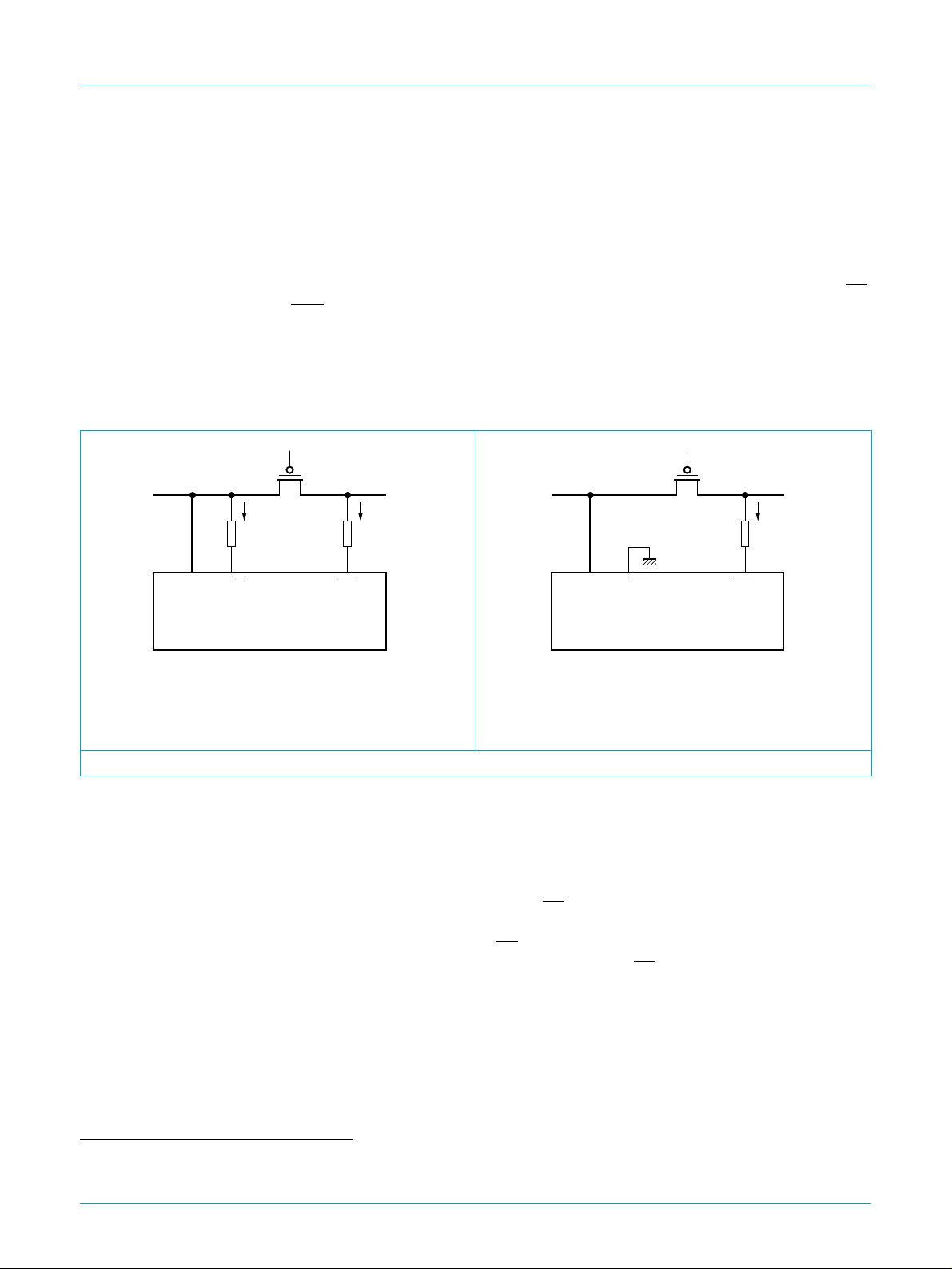
or OCn (see Figure 9). Rtu tunes up the trip voltage ∆V
according to Equation 1.
ISP1122A
USB stand-alone hub
) of 85 mV. This gives a typical trip current of approximately 850 mA for
trip
and Rtd tunes it down
trip
handbook, halfpage
V
CC
I
=5µA
ref(nom)
I
= 0.5 µA
OC(nom)
VCCSP/BP
∆V
with I
I
ref
R
tu
ISP1122A
trip
ref(nom)
low-ohmic
PMOS switch
OCn
∆V
trip intrinsic()IrefRtu
=5µA and I
I
OC
R
td
MBL167
OC(nom)
⋅ IOCRtd⋅–+=
= 0.5 µA.
handbook, halfpage
V
BUS
I
OC(nom)
VCCSP/BP
= 0.5 µA
a. Self-powered mode. b. Bus-powered mode.
Fig 9. Tuning the overcurrent trip voltage.
12.4 Reference circuits
ISP1122A
low-ohmic
PMOS switch
R
OCn
MBL168
(1)
I
OC
td
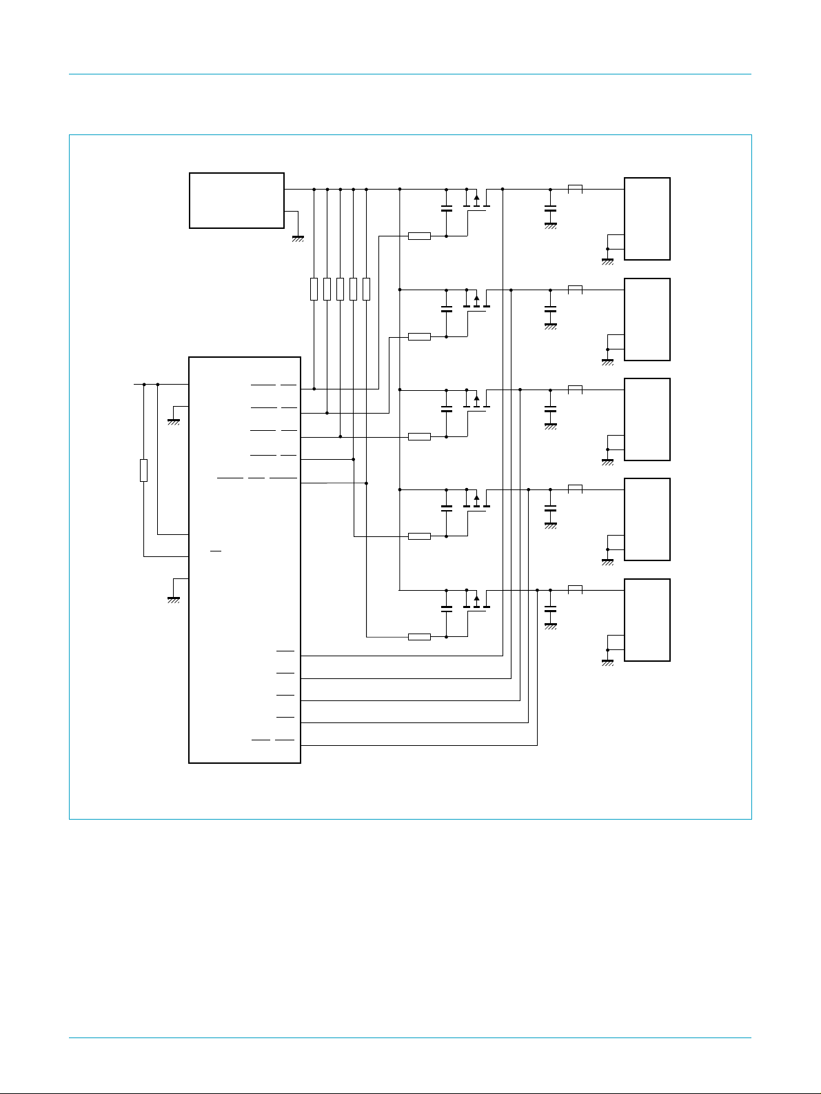
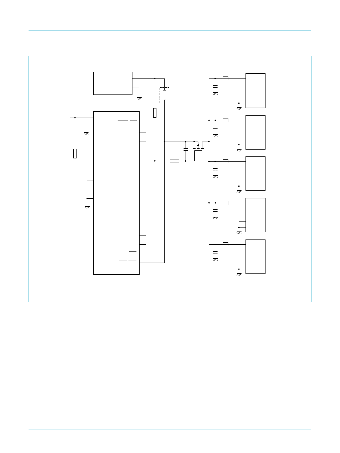
Some typical examples of port power switching and overcurrent detection modes are
given in Figure 10 to Figure 13.
The RC circuit (47 kΩ and 0.1 µF) around the PMOS switch provides for soft turn-on.
The series resistor connecting the SP/BP pin to VCC tunes up the overcurrent trip
voltage slightly (see Figure 9). In the schematic diagram the resistor separates the
net names for pins VCC and SP/BP. This allows an automatic router to use a wide
trace for VCC and a narrow trace to connect pin SP/BP.
1. The following PMOS power switches have been tested to work well with the ISP1122A: Philips PHP109, Vishay Siliconix Si2301DS,
Fairchild FDN338P.
9397 750 08958
Product data Rev. 03 — 30 October 2001 25 of 48
© Koninklijke Philips Electronics N.V. 2001. All rights reserved.
Page 26
Philips Semiconductors
ISP1122A
USB stand-alone hub
handbook, full pagewidth
+4.85 V(min)
100 Ω
to
1 kΩ
5 V
POWER SUPPLY
± 3%
V
CC
GND
INDV
SP/BP
OPTION
PSW1/GL1
PSW2/GL2
PSW3/GL3
PSW4/GL4
PSW5/GL5/GPSW
ISP1122A
OC5/GOC
+4.85 V(min)
+
−
330 kΩ
(5×)
OC1
OC2
OC3
OC4
0.1 µF
47 kΩ
0.1 µF
47 kΩ
0.1 µF
47 kΩ
0.1 µF
47 kΩ
0.1 µF
47 kΩ
low-ohmic
PMOS switch
low-ohmic
PMOS switch
low-ohmic
PMOS switch
low-ohmic
PMOS switch
low-ohmic
PMOS switch
downstream
(min)
(min)
(min)
(min)
(min)
ports
V
BUS
D+
D−
GND
SHIELD
V
BUS
D+
D−
GND
SHIELD
V
BUS
D+
D−
GND
SHIELD
V
BUS
D+
D−
GND
SHIELD
V
BUS
D+
D−
GND
SHIELD
MBL170
1
2
3
4
5
ferrite bead
1
2
3
4
5
+4.75 V
120
µF
ferrite bead
+4.75 V
120
µF
ferrite bead
+4.75 V
120
µF
ferrite bead
+4.75 V
120
µF
ferrite bead
+4.75 V
120
µF
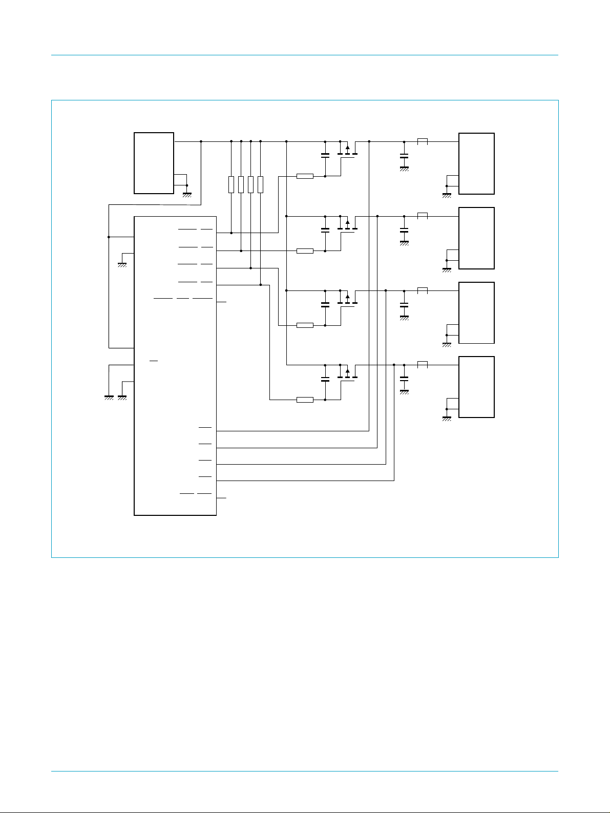
Power switches 1 to 5 are low-ohmic PMOS devices as specified in Section 12.2.
Fig 10. Mode 5: self-powered hub; individual port power switching; individual overcurrent detection.
9397 750 08958
Product data Rev. 03 — 30 October 2001 26 of 48
© Koninklijke Philips Electronics N.V. 2001. All rights reserved.
Page 27
Philips Semiconductors
ISP1122A
USB stand-alone hub
handbook, full pagewidth
+4.95 V(min)
100 Ω
to
1 kΩ
5.1 V KICK-UP
POWER SUPPLY
± 3%
V
CC
GND
INDV
SP/BP
OPTION
PSW1/GL1
PSW2/GL2
PSW3/GL3
PSW4/GL4
PSW5/GL5/GPSW
ISP1122A
OC5/GOC
+4.95 V(min)
+
−
OC1
OC2
OC3
OC4
330
kΩ
low-ohmic
sense resistor
for overcurrent
detection
low-ohmic
PMOS switch
0.1 µF
47 kΩ
ferrite bead
+4.75 V
120
µF
ferrite bead
+4.75 V
120
µF
ferrite bead
+4.75 V
120
µF
ferrite bead
+4.75 V
120
µF
ferrite bead
+4.75 V
120
µF
(min)
(min)
(min)
(min)
(min)
downstream
ports
V
BUS
D+
D−
GND
SHIELD
V
BUS
D+
D−
GND
SHIELD
V
BUS
D+
D−
GND
SHIELD
V
BUS
D+
D−
GND
SHIELD
V
BUS
D+
D−
GND
SHIELD
MBL171
1
2
3
4
5
Power switch is low-ohmic PMOS device as specified in Section 12.2.
Fig 11. Mode 1: self-powered hub; ganged port power switching; global overcurrent detection.
9397 750 08958
Product data Rev. 03 — 30 October 2001 27 of 48
© Koninklijke Philips Electronics N.V. 2001. All rights reserved.
Page 28
Philips Semiconductors
ISP1122A
USB stand-alone hub
handbook, full pagewidth
upstream
port
V
BUS
D+
D−
GND
SHIELD
V
CC
GND
PSW5/GL5/GPSW
INDV
SP/BP
OPTION
ISP1122A
+4.50 V(min)
330 kΩ
PSW1/GL1
PSW2/GL2
PSW3/GL3
PSW4/GL4
OC1
OC2
OC3
OC4
OC5/GOC
(4×)
0.1 µF
47 kΩ
0.1 µF
47 kΩ
0.1 µF
47 kΩ
0.1 µF
47 kΩ
low-ohmic
PMOS switch
low-ohmic
PMOS switch
low-ohmic
PMOS switch
low-ohmic
PMOS switch
downstream
(min)
(min)
(min)
(min)
ports
V
BUS
D+
D−
GND
SHIELD
V
BUS
D+
D−
GND
SHIELD
V
BUS
D+
D−
GND
SHIELD
V
BUS
D+
D−
GND
SHIELD
MBL172
1
2
3
4
ferrite bead
1
2
3
4
+4.40 V
120
µF
ferrite bead
+4.40 V
120
µF
ferrite bead
+4.40 V
120
µF
ferrite bead
+4.40 V
120
µF
Power switches 1 to 4 are low-ohmic PMOS devices as specified in Section 12.2.
Fig 12. Mode 4: bus-powered hub; individual port power switching; individual overcurrent detection.
9397 750 08958
Product data Rev. 03 — 30 October 2001 28 of 48
© Koninklijke Philips Electronics N.V. 2001. All rights reserved.
Page 29
Philips Semiconductors
ISP1122A
USB stand-alone hub
handbook, full pagewidth
upstream
port
V
BUS
D+
D−
GND
SHIELD
V
CC
GND
INDV
SP/BP
OPTION
PSW2/GL2
PSW3/GL3
PSW4/GL4
PSW5/GL5/GPSW
ISP1122A
+4.50 V(min)
PSW1/GL1
OC1
OC2
OC3
OC4
OC5/GOC
330
kΩ
0.1 µF
47 kΩ
low-ohmic
PMOS switch
ferrite bead
+4.40 V
120
µF
ferrite bead
+4.40 V
120
µF
ferrite bead
+4.40 V
120
µF
ferrite bead
+4.40 V
120
µF
(min)
(min)
(min)
(min)
downstream
ports
V
BUS
D+
D−
GND
SHIELD
V
BUS
D+
D−
GND
SHIELD
V
BUS
D+
D−
GND
SHIELD
V
BUS
D+
D−
GND
SHIELD
MBL173
1
2
3
4
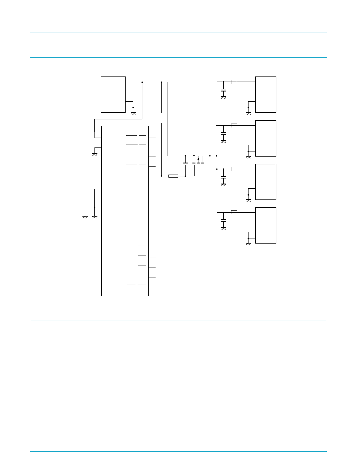
Power switch is low-ohmic PMOS device as specified in Section 12.2.
Fig 13. Mode 0: bus-powered hub; ganged port power switching; global overcurrent detection.
9397 750 08958
Product data Rev. 03 — 30 October 2001 29 of 48
© Koninklijke Philips Electronics N.V. 2001. All rights reserved.
Page 30

Philips Semiconductors
ISP1122A
USB stand-alone hub
13. Limiting values
Table 24: Absolute maximum ratings
In accordance with the Absolute Maximum Rating System (IEC 60134).
Symbol Parameter Conditions Min Max Unit
V
CC
V
I
I
latchup
V
esd
T
stg
P
tot
[1] Equivalent to discharging a 100 pF capacitor via a 1.5 kΩ resistor (Human Body Model).
[2] Values are given for device only; in-circuit V
Table 25: Recommended operating conditions
Symbol Parameter Conditions Min Max Unit
V
CC
V
I
V
I(AI/O)
V
O(od)
T
amb
supply voltage −0.5 +6.0 V
input voltage −0.5 VCC+ 0.5 V
latchup current VI< 0 or VI>V
electrostatic discharge voltage ILI<1µA
CC
- 100 mA
[1][2]
- ±1500 V
storage temperature −60 +150 °C
total power dissipation - 95 mW
= ±8000 V.
esd(max)
supply voltage 4.0 5.5 V
input voltage 0 5.5 V
input voltage on analog I/O pins
0 3.6 V
(D+/D−)
open-drain output pull-up voltage 0 5.5 V
operating ambient temperature −40 +85 °C
9397 750 08958
Product data Rev. 03 — 30 October 2001 30 of 48
© Koninklijke Philips Electronics N.V. 2001. All rights reserved.
Page 31

Philips Semiconductors
ISP1122A
USB stand-alone hub
14. Static characteristics
Table 26: Static characteristics; supply pins
VCC= 4.0 to 5.5 V; V
Symbol Parameter Conditions Min Typ Max Unit
V
reg(3.3)
I
CC
) suspend supply current 1.5 kΩ pull-up on upstream
I
CC(susp
[1] In ‘suspend’ mode the minimum voltage is 2.7 V.
regulated supply voltage 3.0
operating supply current - 18 - mA
Table 27: Static characteristics: digital pins
VCC= 4.0 to 5.5 V; V
Symbol Parameter Conditions Min Typ Max Unit
Input levels
V
IL
V
IH
LOW-level input voltage - - 0.8 V
HIGH-level input voltage 2.0 - - V
Schmitt trigger inputs
V
th(LH)
positive-going threshold
voltage
V
th(HL)
negative-going threshold
voltage
V
hys
hysteresis voltage 0.4 - 0.7 V
Output levels
V
OL
LOW-level output voltage
(open drain outputs)
Leakage current
I
LI
input leakage current - - ±1 µA
Open-drain outputs
I
OZ
OFF-state output current - - ±1 µA
GND
GND
=0V; T
=0V; T
=−40 to+85°C; unless otherwise specified.
amb
port D+ (pin DP0)
no pull-up on upstream port
D+ (pin DP0)
=−40 to+85°C; unless otherwise specified.
amb
IOL= 6 mA - - 0.4 V
=20µA - - 0.1 V
I
OL
[1]
3.3 3.6 V
- - 270 µA
--80µA
1.4 - 1.9 V
0.9 - 1.5 V
Table 28: Static characteristics: overcurrent sense pins
VCC= 4.0 to 5.5 V; V
GND
=0V; T
=−40 to+85°C; unless otherwise specified.
amb
Symbol Parameter Conditions Min Typ Max Unit
∆V
trip
[1] Bus-powered mode.
[2] Self-powered or hybrid-powered mode.
9397 750 08958
Product data Rev. 03 — 30 October 2001 31 of 48
overcurrent detection
trip voltage on
OCn pins
∆V=V
∆V=V
CC
SP/BP
− V
OCn
− V
OCn
[1]
65 85 105 mV
[2]
© Koninklijke Philips Electronics N.V. 2001. All rights reserved.
Page 32

Philips Semiconductors
ISP1122A
USB stand-alone hub
Table 29: Static characteristics: analog I/O pins (D+, D−)
VCC= 4.0 to 5.5 V; V
GND
=0V; T
=−40 to+85°C; unless otherwise specified.
amb
[1]
Symbol Parameter Conditions Min Typ Max Unit
Input levels
V
DI
V
CM
differential input sensitivity |V
differential common mode
− V
I(D+)
| 0.2 - - V
I(D−)
includes VDI range 0.8 - 2.5 V
voltage
V
IL
V
IH
LOW-level input voltage - - 0.8 V
HIGH-level input voltage 2.0 - - V
Output levels
V
OL
V
OH
LOW-level output voltage RL= 1.5 kΩ to +3.6V - - 0.3 V
HIGH-level output voltage RL=15kΩ to GND 2.8 - 3.6 V
Leakage current
I
LZ
OFF-state leakage current - - ±10 µA
Capacitance
C
IN
transceiver capacitance pin to GND - - 20 pF
Resistance
[2]
Z
DRV
Z
INP
driver output impedance steady-state drive 28 - 44 Ω
input impedance 10 - - MΩ
Termination
V
TERM
[3]
termination voltage for
upstream port pull-up (R
PU
)
3.0
[4]
- 3.6 V
[1] D+ is the USB positive data pin (DPn); D− is the USB negative data pin (DMn).
[2] Includes external resistors of 20 Ω±1% on both D+ and D−.
[3] This voltage is available at pin V
[4] In ‘suspend’ mode the minimum voltage is 2.7 V.
reg(3.3)
.
15. Dynamic characteristics
Table 30: Dynamic characteristics
VCC= 4.0 to 5.5 V; V
Symbol Parameter Conditions Min Typ Max Unit
Reset
t
W(RESET)
pulse width on input RESET crystal oscillator running 10 - - µs
Crystal oscillator
f
XTAL
[1] Dependent on the crystal oscillator start-up time.
crystal frequency - 6 - MHz
GND
=0V; T
=−40 to+85°C; unless otherwise specified.
amb
crystal oscillator stopped - 2
[1]
-ms
9397 750 08958
Product data Rev. 03 — 30 October 2001 32 of 48
© Koninklijke Philips Electronics N.V. 2001. All rights reserved.
Page 33

Philips Semiconductors
ISP1122A
USB stand-alone hub
Table 31: Dynamic characteristics: overcurrent sense pins
VCC= 4.0 to 5.5 V; V
Symbol Parameter Conditions Min Typ Max Unit
t
trip
overcurrent trip response time
from
[1] Operating modes 0, 1, 4 and 5; see Table 4.
GND
=0V; T
=−40 to+85°C; unless otherwise specified.
amb
OCn LOW to PSWn HIGH
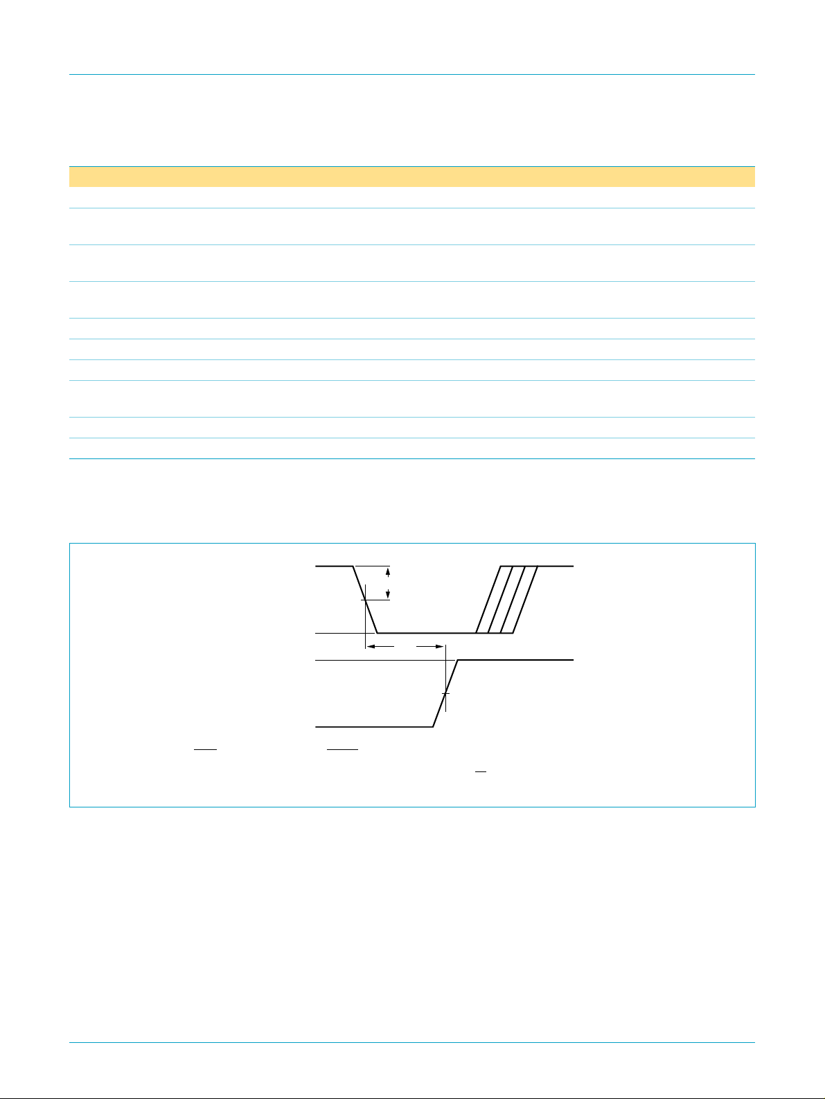
see Figure 14
[1]
--15ms
Table 32: Dynamic characteristics: analog I/O pins (D+, D−); full-speed mode
VCC= 4.0 to 5.5 V; V
GND
=0V;T
=−40 to+85°C; CL= 50 pF; RPU= 1.5 kΩon D+to V
amb
[1]
.; unless otherwise specified.
TERM
Symbol Parameter Conditions Min Typ Max Unit
Driver characteristics
t
FR
t
FF
rise time CL=50pF;
fall time CL=50pF;
FRFM differential rise/fall time
V
CRS
matching (t
output signal crossover voltage
FR/tFF
)
10 to 90% of |V
10 to 90% of |V
OH
OH
− VOL|
− VOL|
4 - 20 ns
4 - 20 ns
[2]
90 - 111.11 %
[2][3]
1.3 - 2.0 V
Data source timing
t
DJ1
source differential jitter for
see Figure 15
[2][3]
−3.5 - +3.5 ns
consecutive transitions
t
DJ2
source differential jitter for
see Figure 15
[2][3]
−4- +4ns
paired transitions
t
FEOPT
t
FDEOP
source EOP width see Figure 16
sourcedifferentialdata-to-EOP
see Figure 16
[3]
160 - 175 ns
[3]
−2- +5ns
transition skew
Receiver timing
t
JR1
receiverdata jitter tolerance for
see Figure 17
[3]
−18.5 - +18.5 ns
consecutive transitions
t
JR2
receiverdata jitter tolerance for
see Figure 17
[3]
−9- +9ns
paired transitions
t
FEOPR
receiver SE0 width accepted as EOP;
[3]
82--ns
see Figure 16
t
FST
width of SE0 during differential
transition
rejected as EOP;
see Figure 18
[3]
--14ns
Hub timing (downstream ports configured as full-speed)
t
FHDD
t
FSOP
hub differential data delay
(without cable)
data bit width distortion after
see Figure 19;
=0pF
C
L
see Figure 19
[3]
--44ns
[3]
−5- +5ns
SOP
t
FEOPD
t
FHESK
hub EOP delay relative to t
HDD
see Figure 20
hub EOP output width skew see Figure 20
[3]
0 - 15 ns
[3]
−15 - +15 ns
[1] Test circuit: see Figure 22.
[2] Excluding the first transition from Idle state.
[3] Characterized only, not tested. Limits guaranteed by design.
9397 750 08958
Product data Rev. 03 — 30 October 2001 33 of 48
© Koninklijke Philips Electronics N.V. 2001. All rights reserved.
Page 34
Philips Semiconductors
ISP1122A
USB stand-alone hub
Table 33: Dynamic characteristics: analog I/O pins (D+, D−); low-speed mode
VCC= 4.0 to 5.5 V; V
GND
=0V;T
=−40 to+85°C; CL= 50 pF; RPU= 1.5 kΩon D−to V
amb
[1]
; unless otherwise specified.
TERM
Symbol Parameter Conditions Min Typ Max Unit
Driver characteristics
t
LR
t
LF
rise time CL= 200 to 600 pF;
fall time CL= 200 to 600 pF;
LRFM differential rise/fall time
V
CRS
matching (t
output signal crossover voltage
LR/tLF
)
10 to 90% of |V
10 to 90% of |V
OH
OH
− VOL|
− VOL|
75 - 300 ns
75 - 300 ns
[2]
80 - 125 %
[2][3]
1.3 - 2.0 V
Hub timing (downstream ports configured as low-speed)
t
LHDD
t
LSOP
hub differential data delay see Figure 19 - - 300 ns
data bit width distortion after
see Figure 19
[3]
−60 - +60 ns
SOP
t
LEOPD
t
LHESK
[1] Test circuit: see Figure 22.
[2] Excluding the first transition from Idle state.
[3] Characterized only, not tested. Limits guaranteed by design.
hub EOP delay relative to t
HDD
see Figure 20
hub EOP output width skew see Figure 20
[3]
0 - 200 ns
[3]
−300 - +300 ns
V
CC
overcurrent
input
0 V
V
CC
power switch
output
0 V
Overcurrent input: OCn; power switch output: PSWn.
Reference voltage for overcurrent sensing: VCC (bus-powered mode) or V
∆V
trip
t
trip
Fig 14. Overcurrent trip response timing.
(self-powered mode).
SP/BP
MBL032
9397 750 08958
Product data Rev. 03 — 30 October 2001 34 of 48
© Koninklijke Philips Electronics N.V. 2001. All rights reserved.
Page 35
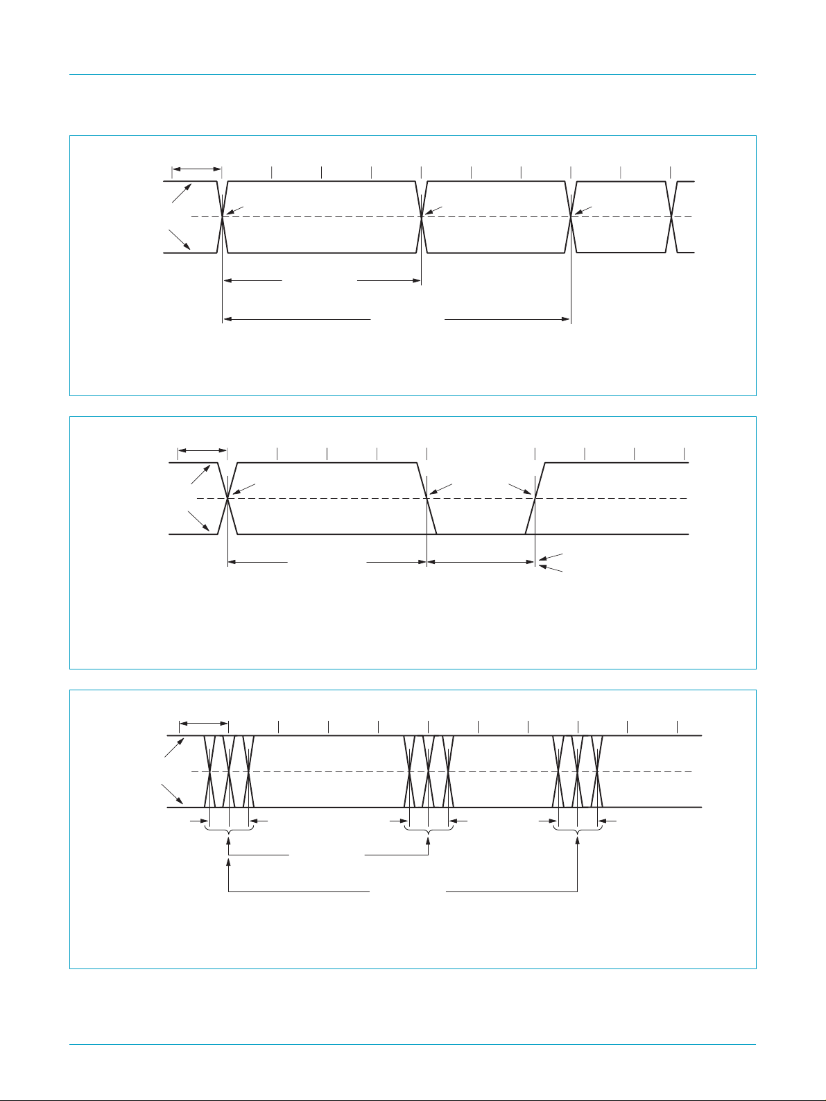
Philips Semiconductors
T
PERIOD
+3.3 V
differential
data lines
crossover point
ISP1122A
USB stand-alone hub
crossover point crossover point
0 V
consecutive
transitions
N × T
T
is the bit duration corresponding with the USB data rate.
PERIOD
PERIOD
+ t
DJ1
N × T
paired
transitions
PERIOD
+ t
DJ2
Fig 15. Source differential data jitter.
T
PERIOD
+3.3 V
differential
data lines
0 V
T
is the bit duration corresponding with the USB data rate.
PERIOD
crossover point
differential data to
SE0/EOP skew
N × T
PERIOD
+ t
DEOP
crossover point
extended
Full-speed timing symbols have a subscript prefix ‘F’, low-speed timings a prefix ‘L’.
Fig 16. Source differential data-to-EOP transition skew and EOP width.
source EOP width: t
receiver EOP width: t
MGR870
EOPT
EOPR
MGR776
T
PERIOD
+3.3 V
differential
data lines
0 V
T
is the bit duration corresponding with the USB data rate.
PERIOD
t
JR
N × T
consecutive
transitions
PERIOD
+ t
JR1
N × T
paired
transitions
PERIOD
+ t
JR2
t
JR1
t
JR2
MGR871
Fig 17. Receiver differential data jitter.
9397 750 08958
Product data Rev. 03 — 30 October 2001 35 of 48
© Koninklijke Philips Electronics N.V. 2001. All rights reserved.
Page 36
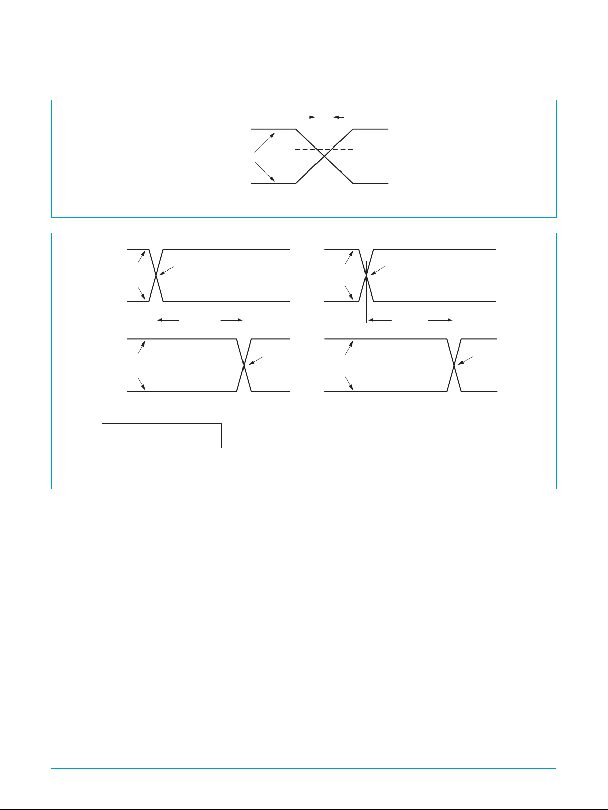
Philips Semiconductors
+3.3 V
t
FST
ISP1122A
USB stand-alone hub
Fig 18. Receiver SE0 width tolerance.
+3.3 V
upstream
differential
data lines
0 V
+3.3 V
downstream
differential
data lines
0 V
SOP distortion:
t
= t
SOP
HDD (next J)
(A) downstream hub delay (B) upstream hub delay
crossover
point
hub delay
downstream
t
HDD
− t
HDD(SOP)
differential
data lines
0 V
crossover
point
downstream
differential
data
upstream
differential
data
V
IH(min)
MGR872
crossover
point
hub delay
upstream
t
HDD
crossover
point
MGR777
Full-speed timing symbols have a subscript prefix ‘F’, low-speed timings a prefix ‘L’.
Fig 19. Hub differential data delay and SOP distortion.
9397 750 08958
© Koninklijke Philips Electronics N.V. 2001. All rights reserved.
Product data Rev. 03 — 30 October 2001 36 of 48
Page 37
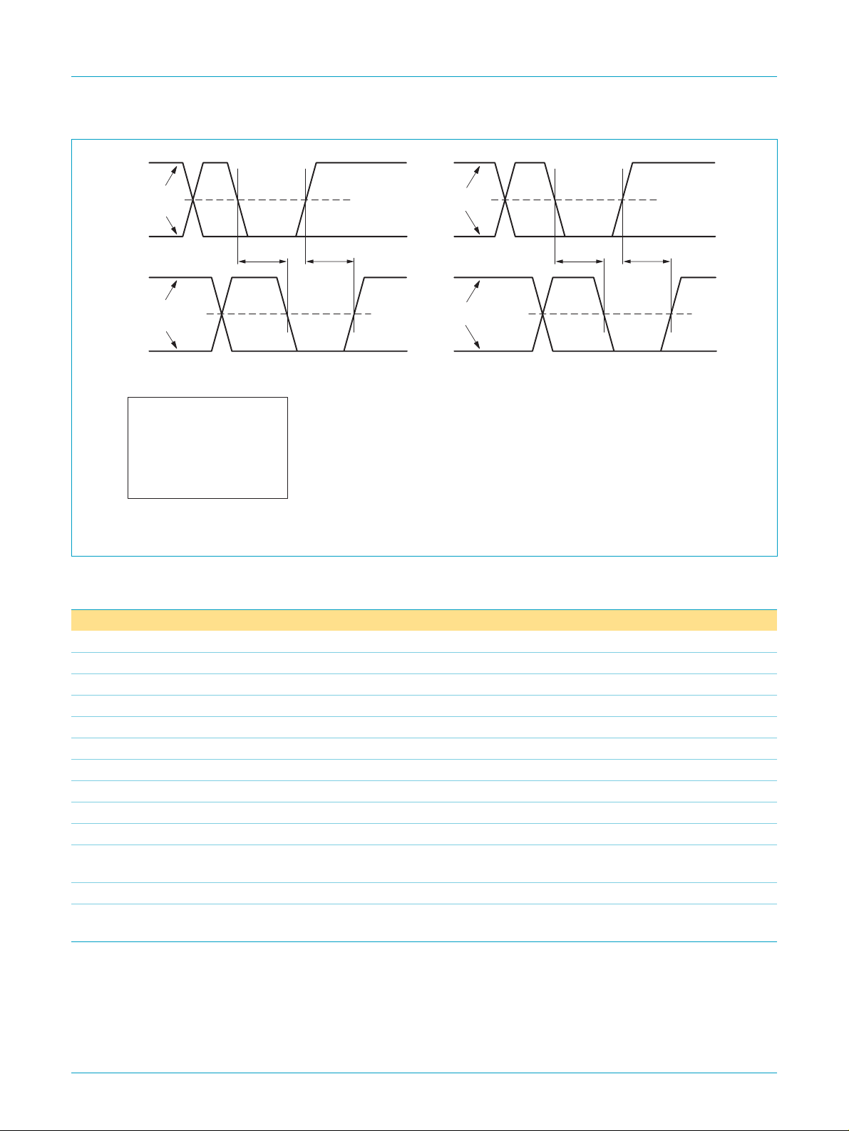
Philips Semiconductors
+3.3 V
ISP1122A
USB stand-alone hub
t
EOP+
crossover
point
extended
crossover
extended
MGR778
point
upstream
differential
data lines
0 V
+3.3 V
downstream
differential
data lines
0 V
EOP delay:
t
= max (t
EOP
EOP delay relative to t
t
= t
EOPD
EOP skew:
t
= t
HESK
crossover
point
extended
t
EOP−
(A) downstream EOP delay (B) upstream EOP delay
, t
HDD
HDD
EOP−
EOP+
:
)
EOP
EOP+
EOP−
− t
− t
t
EOP+
crossover
point
extended
downstream
port
upstream
end of cable
t
EOP−
Full-speed timing symbols have a subscript prefix ‘F’, low-speed timings a prefix ‘L’.
Fig 20. Hub EOP delay and EOP skew.
Table 34: Dynamic characteristics: I2C-bus pins (SDA, SCL)
VCC and T
within recommended operating range; V
amb
=
+5 V; VSS=V
DD
; VIL and VIH between VSS and VDD.
GND
Symbol Parameter Conditions Min Typ Max Unit
f
SCL
t
BUF
t
SU;STA
t
HD;STA
t
LOW
t
HIGH
t
r
t
f
t
SU;DAT
t
HD;DAT
t
VD;DAT
SCL clock frequency f
= 6 MHz 0 93.75
XTAL
bus free time 4.7 - - µs
START condition set-up time 250 - - ns
hold time START condition 4.0 - - µs
SCL LOW time 4.7 - - µs
SCL HIGH time 4.0 - - µs
SCL and SDA rise time
[2]
- - 1000 ns
SCL and SDA fall time - - 300 ns
data set-up time 250 - - ns
data hold time 0 - - µs
SCL LOW to data out valid
- - 0.4 µs
[1]
100 kHz
time
t
SU;STO
C
b
STOP condition set-up time 4.0 - - µs
capacitive load for each bus
- - 400 pF
line
[1] f
SCL
=1⁄64f
XTAL
.
[2] Rise time is determined by Cb and pull-up resistor value Rp (typ. 4.7 kΩ).
9397 750 08958
© Koninklijke Philips Electronics N.V. 2001. All rights reserved.
Product data Rev. 03 — 30 October 2001 37 of 48
Page 38
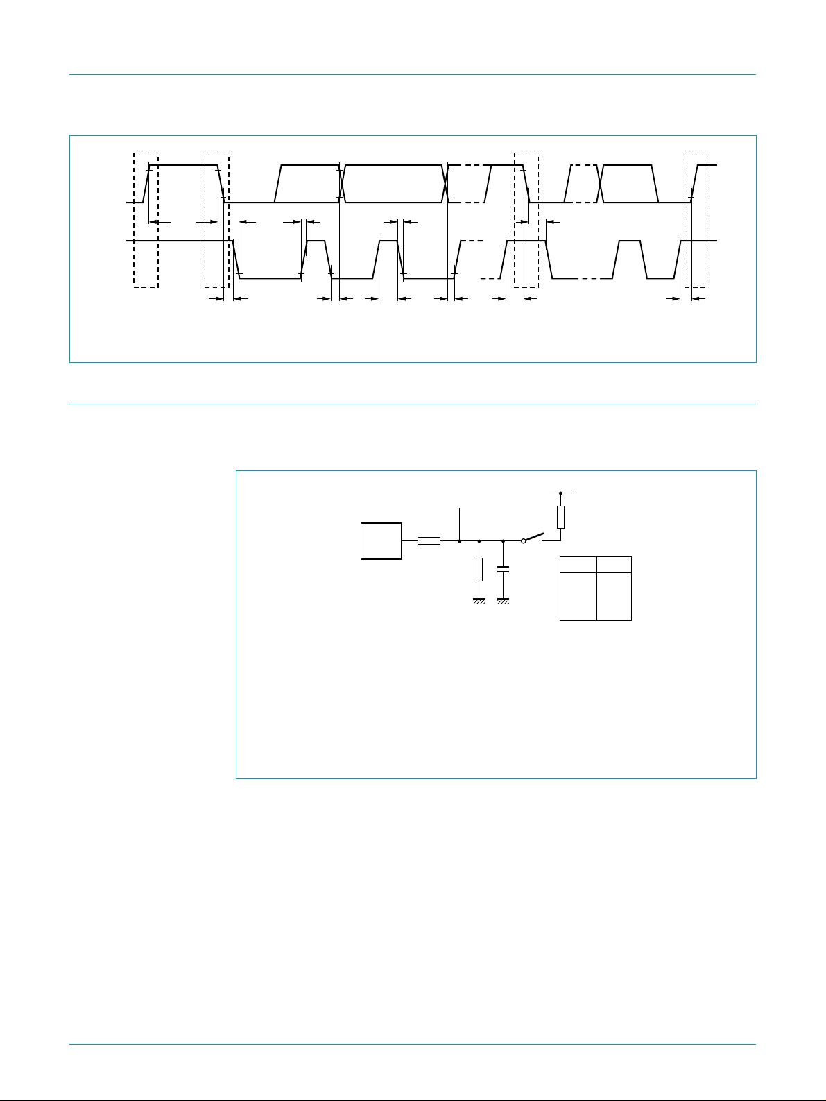
Philips Semiconductors
SDA
ISP1122A
USB stand-alone hub
t
BUF
SCL
P
S S
t
HD;STA
Fig 21. I2C-bus timing.
16. Test information
The dynamic characteristics of the analog I/O ports (D+ and D−) as listed in Table 32
and Table 33, were determined using the circuit shown in Figure 22.
t
LOW
t
r
t
HD;STA
t
HIGH
D.U.T.
t
f
20 Ω
t
SU;DAT
test point
15 kΩ
t
SU;STA
C
t
HD;STA
P
t
SU;STO
MGR779
V
reg(3.3)
R
PU
S1
L
1.5 kΩ
test
D−/LS
D+/LS
D−/FS
D+/FS
S1
closed
open
open
closed
MGR775
Load capacitance:
CL= 50 pF (full-speed mode)
CL= 200 pF or 600 pF (low-speed mode, minimum or maximum timing).
Speed selection:
full-speed mode (FS): 1.5 kΩ pull-up resistor on D+
low-speed mode (LS): 1.5 kΩ pull-up resistor on D−.
Fig 22. Load impedance for D+ and D- pins.
9397 750 08958
Product data Rev. 03 — 30 October 2001 38 of 48
© Koninklijke Philips Electronics N.V. 2001. All rights reserved.
Page 39
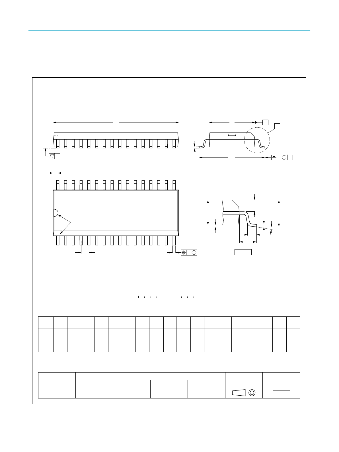
Philips Semiconductors
17. Package outline
ISP1122A
USB stand-alone hub
SO32: plastic small outline package; 32 leads; body width 7.5 mm
D
y
Z
32
pin 1 index
1
e
17
16
w M
b
p
SOT287-1
E
c
H
E
A
2
A
1
detail X
A
X
v M
A
Q
(A )
L
p
L
A
3
θ
0 5 10 mm
scale
DIMENSIONS (inch dimensions are derived from the original mm dimensions)
UNIT
inches
Note
1. Plastic or metal protrusions of 0.15 mm maximum per side are not included.
A
A1A2A3b
max.
0.3
mm
2.65
0.10
OUTLINE
VERSION
SOT287-1 MO-119
0.1
0.012
0.004
2.45
0.25
2.25
0.096
0.01
0.086
IEC JEDEC EIAJ
0.49
0.36
0.02
0.01
p
0.011
0.007
0.27
0.18
(1)E(1)
cD
20.7
20.3
0.81
0.80
REFERENCES
eHELLpQZywv θ
7.6
7.4
0.30
0.29
1.27
0.050
10.65
10.00
0.419
0.394
1.4
0.055
1.1
0.4
0.043
0.016
1.2
1.0
0.047
0.039
0.25 0.1
0.25
0.010.01
EUROPEAN
PROJECTION
0.004
ISSUE DATE
(1)
0.95
0.55
0.037
0.022
97-05-22
99-12-27
o
8
o
0
Fig 23. SO32 package outline.
9397 750 08958
Product data Rev. 03 — 30 October 2001 39 of 48
© Koninklijke Philips Electronics N.V. 2001. All rights reserved.
Page 40
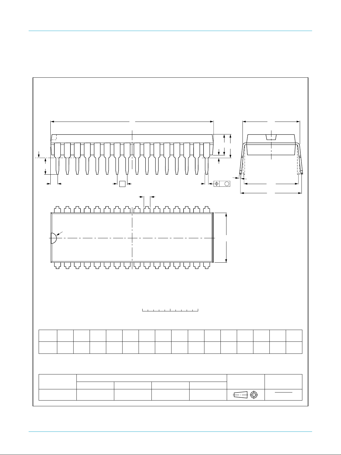
Philips Semiconductors
ISP1122A
USB stand-alone hub
SDIP32: plastic shrink dual in-line package; 32 leads (400 mil)
D
seating plane
L
Z
32
pin 1 index
e
b
SOT232-1
M
E
A
2
A
A
1
w M
b
1
17
E
c
(e )
M
1
H
1
0 5 10 mm
scale
DIMENSIONS (mm are the original dimensions)
A
A
A
UNIT b
Note
1. Plastic or metal protrusions of 0.25 mm maximum per side are not included.
mm
OUTLINE
VERSION
SOT232-1
max.
4.7 0.51 3.8
12
min.
max.
IEC JEDEC EIAJ
1.3
0.8
b
1
0.53
0.40
REFERENCES
0.32
0.23
cEe M
(1) (1)
D
29.4
28.5
9.1
8.7
16
(1)
Z
L
3.2
2.8
EUROPEAN
PROJECTION
M
10.7
10.2
E
12.2
10.5
e
1
H
ISSUE DATE
w
0.181.778 10.16
92-11-17
95-02-04
max.
1.6
Fig 24. SDIP32 package outline.
9397 750 08958
Product data Rev. 03 — 30 October 2001 40 of 48
© Koninklijke Philips Electronics N.V. 2001. All rights reserved.
Page 41
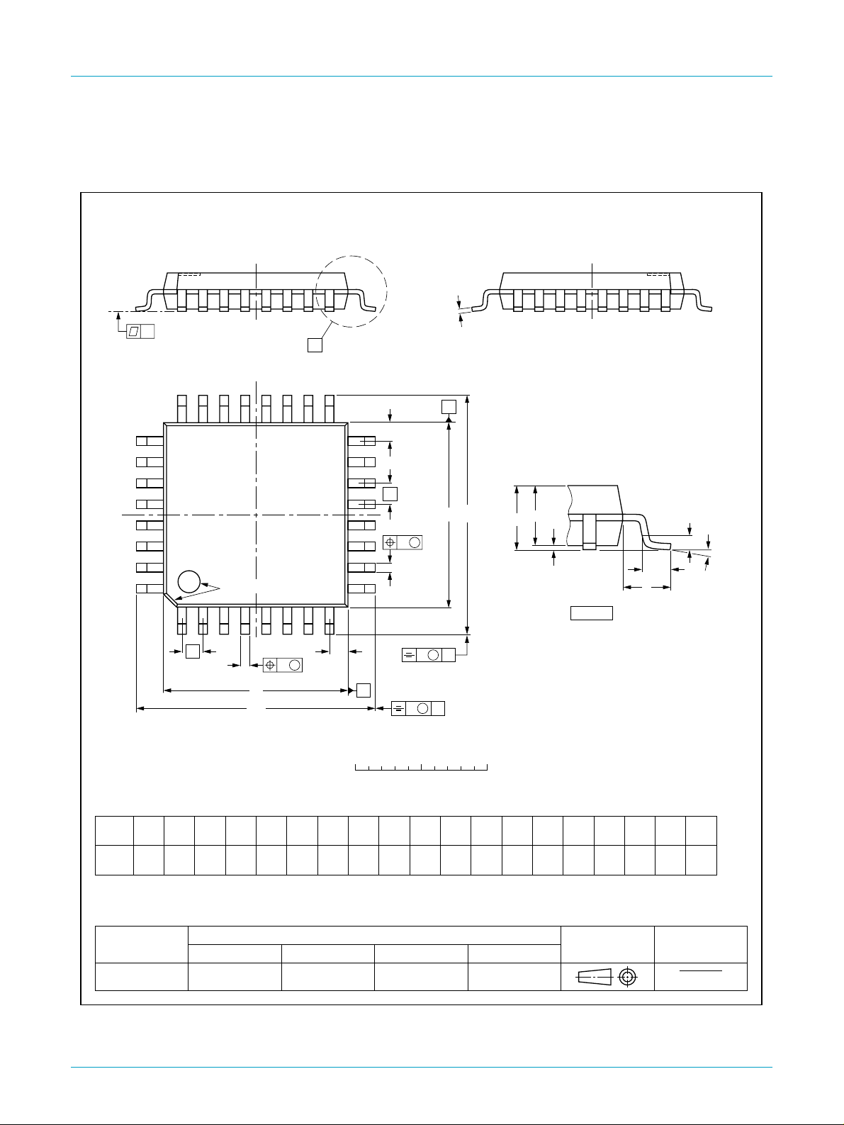
Philips Semiconductors
ISP1122A
USB stand-alone hub
LQFP32: plastic low profile quad flat package; 32 leads; body 7 x 7 x 1.4 mm
c
y
X
24 17
25
pin 1 index
32
1
16
Z
E
e
w M
b
p
9
8
A
H
E
E
A
2
A
SOT358-1
(A )
A
1
L
detail X
3
θ
L
p
e
DIMENSIONS (mm are the original dimensions)
A
UNIT
mm
Note
1. Plastic or metal protrusions of 0.25 mm maximum per side are not included.
OUTLINE
VERSION
SOT358 -1 136E03 MS-026
A1A2A3bpcE
max.
0.20
1.45
1.60
0.05
0.25
1.35
IEC JEDEC EIAJ
w M
b
p
D
H
D
0.4
0.3
Z
D
B
0 2.5 5 mm
(1)
(1) (1)(1)
D
7.1
0.18
0.12
7.1
6.9
6.9
REFERENCES
v M
A
v M
B
scale
eHELL
0.8
H
9.15
8.85
D
9.15
8.85
p
0.75
0.45
0.25 0.11.0 0.2
EUROPEAN
PROJECTION
Z
0.9
0.5
D
Zywv θ
E
0.9
0.5
ISSUE DATE
99-12-27
00-01-19
o
7
o
0
Fig 25. LQFP32 package outline.
9397 750 08958
Product data Rev. 03 — 30 October 2001 41 of 48
© Koninklijke Philips Electronics N.V. 2001. All rights reserved.
Page 42

Philips Semiconductors
18. Soldering
18.1 Introduction
This text gives a very brief insight to a complex technology. A more in-depth account
of soldering ICs can be found in our
Packages
There is no soldering method that is ideal for all IC packages. Wavesoldering is often
preferred when through-hole and surface mount components are mixed on one
printed-circuit board. Wave soldering can still be used for certain surface mount ICs,
but it is not suitable for fine pitch SMDs. In these situations reflow soldering is
recommended.
18.2 Surface mount packages
18.2.1 Reflow soldering
Reflow soldering requires solder paste (a suspension of fine solder particles, flux and
binding agent) to be applied to the printed-circuit board by screen printing, stencilling
or pressure-syringe dispensing before package placement.
ISP1122A
USB stand-alone hub
Data Handbook IC26; Integrated Circuit
(document order number 9398 652 90011).
Several methods exist for reflowing; for example, convection or convection/infrared
heating in a conveyor type oven. Throughput times (preheating, soldering and
cooling) vary between 100 and 200 seconds depending on heating method.
Typical reflow peak temperatures range from 215 to 250 °C. The top-surface
temperature of the packages should preferable be kept below 220 °C for thick/large
packages, and below 235 °C for small/thin packages.
18.2.2 Wave soldering
Conventional single wave soldering is not recommended for surface mount devices
(SMDs) or printed-circuit boards with a high component density, as solder bridging
and non-wetting can present major problems.
To overcome these problems the double-wave soldering method was specifically
developed.
If wave soldering is used the following conditions must be observed for optimal
results:
Use a double-wave soldering method comprising a turbulent wave with high
•
upward pressure followed by a smooth laminar wave.
For packages with leads on two sides and a pitch (e):
•
– larger than or equal to 1.27 mm, the footprint longitudinal axis is preferred to be
parallel to the transport direction of the printed-circuit board;
– smaller than 1.27 mm, the footprint longitudinal axis must be parallel to the
transport direction of the printed-circuit board.
The footprint must incorporate solder thieves at the downstream end.
9397 750 08958
Product data Rev. 03 — 30 October 2001 42 of 48
© Koninklijke Philips Electronics N.V. 2001. All rights reserved.
Page 43

Philips Semiconductors
•
During placement and before soldering, the package must be fixed with a droplet of
adhesive. The adhesive can be applied by screen printing, pin transfer or syringe
dispensing. The package can be soldered after the adhesive is cured.
Typical dwell time is 4 seconds at 250 °C. A mildly-activated flux will eliminate the
need for removal of corrosive residues in most applications.
18.2.3 Manual soldering
Fix the component by first soldering two diagonally-opposite end leads. Use a low
voltage (24 V or less) soldering iron applied to the flat part of the lead. Contact time
must be limited to 10 seconds at up to 300 °C.
When using a dedicated tool, all other leads can be soldered in one operation within
2 to 5 seconds between 270 and 320 °C.
ISP1122A
USB stand-alone hub
For packages with leads on four sides, the footprint must be placed at a 45° angle
to the transport direction of the printed-circuit board. The footprint must
incorporate solder thieves downstream and at the side corners.
18.3 Through-hole mount packages
18.3.1 Soldering by dipping or by solder wave
The maximum permissible temperature of the solder is 260 °C; solder at this
temperature must not be in contact with the joints for more than 5 seconds. The total
contact time of successive solder waves must not exceed 5 seconds.
The device may be mounted up to the seating plane, but the temperature of the
plastic body must not exceed the specified maximum storage temperature (T
If the printed-circuit board has been pre-heated, forced cooling may be necessary
immediately after soldering to keep the temperature within the permissible limit.
18.3.2 Manual soldering
Apply the soldering iron (24 V or less) to the lead(s) of the package, either below the
seating plane or not more than 2 mm aboveit. If the temperature of the soldering iron
bit is less than 300 °C it may remain in contact for up to 10 seconds. If the bit
temperature is between 300 and 400 °C, contact may be up to 5 seconds.
stg(max)
).
9397 750 08958
Product data Rev. 03 — 30 October 2001 43 of 48
© Koninklijke Philips Electronics N.V. 2001. All rights reserved.
Page 44

Philips Semiconductors
18.4 Package related soldering information
Table 35: Suitability of IC packages for wave, reflow and dipping soldering methods
Mounting Package Soldering method
Through-hole
mount
Surface mount BGA, HBGA, LFBGA,
[1] All surface mount (SMD) packages are moisture sensitive. Depending upon the moisture content, the
[2] For SDIP packages, the longitudinal axis must be parallel to the transport direction of the
[3] These packages are not suitable for wave soldering. On versions with the heatsink on the bottom
[4] If wave soldering is considered, then the package must be placed at a 45° angle to the solder wave
[5] Wave soldering is only suitable for LQFP, QFP and TQFP packages with a pitch (e) equal to or larger
[6] Wave soldering is only suitable for SSOP and TSSOP packages with a pitch (e) equal to or larger than
ISP1122A
USB stand-alone hub
Wave Reflow
DBS, DIP, HDIP, SDIP, SIL suitable
[2]
not suitable suitable −
SQFP, TFBGA
HBCC, HLQFP, HSQFP,
not suitable
[3]
HSOP, HTQFP, HTSSOP,
HVQFN, SMS
[4]
PLCC
LQFP, QFP, TQFP not recommended
SSOP, TSSOP, VSO not recommended
maximum temperature (with respect to time) and body size of the package, there is a risk that internal
or external package cracks may occur due to vaporization of the moisture in them (the so called
popcorn effect). For details, refer to the Drypack information in the
Circuit Packages; Section: Packing Methods
printed-circuit board.
side, the solder cannot penetrate between the printed-circuit board and the heatsink. On versions with
the heatsink on the top side, the solder might be deposited on the heatsink surface.
direction. The package footprint must incorporate solder thieves downstream and at the side corners.
than 0.8 mm; it is definitely not suitable for packages with a pitch (e) equal to or smaller than 0.65 mm.
0.65 mm; it is definitely not suitable for packages with a pitch (e) equal to or smaller than 0.5 mm.
, SO, SOJ suitable suitable −
[4][5]
[6]
Data Handbook IC26; Integrated
.
[1]
Dipping
− suitable
suitable −
suitable −
suitable −
9397 750 08958
Product data Rev. 03 — 30 October 2001 44 of 48
© Koninklijke Philips Electronics N.V. 2001. All rights reserved.
Page 45

Philips Semiconductors
ISP1122A
USB stand-alone hub
19. Revision history
Table 36: Revision history
Rev Date CPCN Description
03 20011030 Product data; second version; Supersedes ISP1122A-02 of June 6th, 2000.
(9397 750 07175)
Added new USB basic speed logo to indicate ISP1122A as a USB-IF certified product.
•
Table 24 “Absolute maximum ratings” on page 30:
•
– Changed I
– Changed V
– Removed table note 3.
– Changed I
02 20000606 Product specification; initial version. Supersedes ISP1122A-01 of 27 March 2000
(9397 750 06986).
01 20000327 Preliminary specification; initial version.
latchup
to 1500 V.
esd
to 1 µA.
LI
to 100 mA.
20. Trademarks
ACPI — is an open industry specification for PC power management, co-developed by Intel Corp., Microsoft Corp. and
Toshiba
GoodLink — is a trademark of Koninklijke Philips Electronics N.V.
OnNow — is a trademark of Microsoft Corp.
SMBus — is a bus specification for PC power management, developed by Intel Corp. based on the I
Koninklijke Philips Electronics
SoftConnect — is a trademark of Koninklijke Philips Electronics
2
C-bus from
9397 750 08958
Product data Rev. 03 — 30 October 2001 45 of 48
© Koninklijke Philips Electronics N.V. 2001. All rights reserved.
Page 46

Philips Semiconductors
21. Data sheet status
ISP1122A
USB stand-alone hub
Data sheet status
Objective data Development This data sheet contains data from theobjective specification for product development.Philips Semiconductors
Preliminary data Qualification This data sheet contains data from the preliminary specification. Supplementary data will be published at a
Product data Production This data sheet contains data from the product specification. Philips Semiconductors reserves the right to
[1] Please consult the most recently issued data sheet before initiating or completing a design.
[2] The product status of the device(s) described in this data sheet may have changed since this data sheet was published. The latest information is available on the Internet at
URL http://www.semiconductors.philips.com.
[1]
Product status
[2]
Definition
reserves the right to change the specification in any manner without notice.
later date. Philips Semiconductors reserves the right to change the specification without notice, in order to
improve the design and supply the best possible product.
make changes at any time in order to improve the design, manufacturing and supply. Changes will be
communicated according to the Customer Product/Process Change Notification (CPCN) procedure
SNW-SQ-650A.
22. Definitions
Short-form specification — The data in a short-form specification is extracted from a full data sheet with the same type
number and title. For detailed information see the relevant data sheet or data handbook.
Limiting values definition — Limiting values given are in accordance with the Absolute Maximum Rating System
(IEC 60134). Stress above one or more of the limiting values may cause permanent damage to the device. These are
stress ratings only and operation of the device at these or at any other conditions above those given in the Characteristics
sections of the specification is not implied. Exposure to limiting values for extended periods may affect device reliability.
Application information — Applications that are described herein for any of these products are for illustrative purposes
only. Philips Semiconductors make no representation or warranty that such applications will be suitable for the specified
use without further testing or modification.
23. Disclaimers
Life support — These products are not designed for use in life support appliances, devices, or systems where
malfunction of these products can reasonably be expected to result in personal injury. Philips Semiconductors customers
using or selling these products for use in such applications do so at their own risk and agree to fully indemnify Philips
Semiconductors for any damages resulting from such application.
Right to make changes — Philips Semiconductors reserves the right to make changes, without notice, in the products,
including circuits, standard cells, and/or software, described or contained herein in order to improve design and/or
performance. Philips Semiconductors assumes no responsibility or liability for the use of any of these products, conveys
no licence or title under any patent, copyright, or mask work right to these products, and makes no representations or
warranties that these products are free from patent, copyright, or mask work right infringement, unless otherwise
specified.
24. Licenses
Purchase of Philips I2C components
2
Purchase of Philips I
under the Philips’ I
2
I
C system provided the system conforms to the I2C
specification defined by Philips. This specification can be
ordered using the code 9398 393 40011.
C components conveys a license
2
C patent to use the components in the
9397 750 08958
© Koninklijke Philips Electronics N.V. 2001. All rights reserved.
Product data Rev. 03 — 30 October 2001 46 of 48
Page 47

Philips Semiconductors
ISP1122A
USB stand-alone hub
Contact information
For additional information, please visit http://www.semiconductors.philips.com.
For sales office addresses, send e-mail to: [email protected]. Fax: +31 40 27 24825
9397 750 08958
Product data Rev. 03 — 30 October 2001 47 of 48
© Koninklijke Philips Electronics N.V. 2001. All rights reserved.
Page 48

Philips Semiconductors
Contents
ISP1122A
USB stand-alone hub
1 General description. . . . . . . . . . . . . . . . . . . . . . 2
2 Features . . . . . . . . . . . . . . . . . . . . . . . . . . . . . . . 2
3 Ordering information. . . . . . . . . . . . . . . . . . . . . 3
4 Block diagram . . . . . . . . . . . . . . . . . . . . . . . . . . 3
5 Pinning information. . . . . . . . . . . . . . . . . . . . . . 4
5.1 ISP1122AD (SO32) and ISP1122ANB
(SDIP32) . . . . . . . . . . . . . . . . . . . . . . . . . . . . . 4
5.1.1 Pinning . . . . . . . . . . . . . . . . . . . . . . . . . . . . . . . 4
5.1.2 Pin description . . . . . . . . . . . . . . . . . . . . . . . . . 4
5.2 ISP1122ABD (LQFP32) . . . . . . . . . . . . . . . . . . 7
5.2.1 Pinning . . . . . . . . . . . . . . . . . . . . . . . . . . . . . . . 7
5.2.2 Pin description . . . . . . . . . . . . . . . . . . . . . . . . . 7
6 Functional description . . . . . . . . . . . . . . . . . . . 9
6.1 Analog transceivers . . . . . . . . . . . . . . . . . . . . . 9
6.2 Philips Serial Interface Engine (SIE). . . . . . . . 10
6.3 Hub repeater. . . . . . . . . . . . . . . . . . . . . . . . . . 10
6.4 End-of-frame timers . . . . . . . . . . . . . . . . . . . . 10
6.5 General and individual port controller. . . . . . . 10
6.6 GoodLink . . . . . . . . . . . . . . . . . . . . . . . . . . . . 10
6.7 Bit clock recovery . . . . . . . . . . . . . . . . . . . . . . 10
6.8 Voltage regulator . . . . . . . . . . . . . . . . . . . . . . 10
6.9 PLL clock multiplier. . . . . . . . . . . . . . . . . . . . . 11
6.10 Overcurrent detection . . . . . . . . . . . . . . . . . . . 11
6.11 I
2
C-bus interface. . . . . . . . . . . . . . . . . . . . . . . 11
7 Modes of operation . . . . . . . . . . . . . . . . . . . . . 11
8 Endpoint descriptions. . . . . . . . . . . . . . . . . . . 12
8.1 Hub endpoint 0 (control). . . . . . . . . . . . . . . . . 12
8.2 Hub endpoint 1 (interrupt). . . . . . . . . . . . . . . . 12
9 Host requests. . . . . . . . . . . . . . . . . . . . . . . . . . 13
9.1 Standard requests . . . . . . . . . . . . . . . . . . . . . 13
9.2 Hub specific requests . . . . . . . . . . . . . . . . . . . 14
9.3 Descriptors . . . . . . . . . . . . . . . . . . . . . . . . . . . 16
9.4 Hub responses . . . . . . . . . . . . . . . . . . . . . . . . 19
9.4.1 Get device status . . . . . . . . . . . . . . . . . . . . . . 19
9.4.2 Get configuration . . . . . . . . . . . . . . . . . . . . . . 19
9.4.3 Get interface status. . . . . . . . . . . . . . . . . . . . . 19
9.4.4 Get hub status . . . . . . . . . . . . . . . . . . . . . . . . 19
9.4.5 Get port status . . . . . . . . . . . . . . . . . . . . . . . . 20
9.4.6 Get configuration descriptor . . . . . . . . . . . . . . 21
9.4.7 Get device descriptor . . . . . . . . . . . . . . . . . . . 21
9.4.8 Get hub descriptor . . . . . . . . . . . . . . . . . . . . . 21
9.4.9 Get string descriptor (0) . . . . . . . . . . . . . . . . . 21
9.4.10 Get string descriptor (1) . . . . . . . . . . . . . . . . . 21
9.4.11 Get string descriptor (2) . . . . . . . . . . . . . . . . . 21
10 I
2
C-bus interface . . . . . . . . . . . . . . . . . . . . . . . 21
10.1 Protocol. . . . . . . . . . . . . . . . . . . . . . . . . . . . . . 21
10.2 Hardware connections . . . . . . . . . . . . . . . . . . 22
10.3 Data transfer. . . . . . . . . . . . . . . . . . . . . . . . . . 22
11 Hub power modes . . . . . . . . . . . . . . . . . . . . . . 23
11.1 Voltage drop requirements. . . . . . . . . . . . . . . 23
11.1.1 Self-powered hubs. . . . . . . . . . . . . . . . . . . . . 23
11.1.2 Bus-powered hubs. . . . . . . . . . . . . . . . . . . . . 24
12 Overcurrent detection. . . . . . . . . . . . . . . . . . . 25
12.1 Overcurrent circuit description . . . . . . . . . . . . 25
12.2 Power switch selection. . . . . . . . . . . . . . . . . . 25
12.3 Tuning the overcurrent trip voltage . . . . . . . . 26
12.4 Reference circuits . . . . . . . . . . . . . . . . . . . . . 26
13 Limiting values . . . . . . . . . . . . . . . . . . . . . . . . 31
14 Static characteristics . . . . . . . . . . . . . . . . . . . 32
15 Dynamic characteristics. . . . . . . . . . . . . . . . . 33
16 Test information . . . . . . . . . . . . . . . . . . . . . . . 39
17 Package outline. . . . . . . . . . . . . . . . . . . . . . . . 40
18 Soldering . . . . . . . . . . . . . . . . . . . . . . . . . . . . . 43
18.1 Introduction . . . . . . . . . . . . . . . . . . . . . . . . . . 43
18.2 Surface mount packages . . . . . . . . . . . . . . . . 43
18.2.1 Reflow soldering. . . . . . . . . . . . . . . . . . . . . . . 43
18.2.2 Wave soldering . . . . . . . . . . . . . . . . . . . . . . . 43
18.2.3 Manual soldering . . . . . . . . . . . . . . . . . . . . . . 44
18.3 Through-hole mount packages . . . . . . . . . . . 44
18.3.1 Soldering by dipping or by solder wave . . . . . 44
18.3.2 Manual soldering . . . . . . . . . . . . . . . . . . . . . . 44
18.4 Package related soldering information. . . . . . 45
19 Revision history . . . . . . . . . . . . . . . . . . . . . . . 46
20 Trademarks . . . . . . . . . . . . . . . . . . . . . . . . . . . 46
21 Data sheet status. . . . . . . . . . . . . . . . . . . . . . . 47
22 Definitions . . . . . . . . . . . . . . . . . . . . . . . . . . . . 47
23 Disclaimers . . . . . . . . . . . . . . . . . . . . . . . . . . . 47
24 Licenses. . . . . . . . . . . . . . . . . . . . . . . . . . . . . . 47
© Koninklijke Philips Electronics N.V. 2001.
Printed in The Netherlands
All rights are reserved. Reproduction in whole or in part is prohibited without the prior
written consent of the copyright owner.
The information presented in this document does not form part of any quotation or
contract, is believed to be accurate and reliable and may be changed without notice. No
liability will be accepted by the publisher for any consequence of its use. Publication
thereof does not convey nor imply any license under patent- or other industrial or
intellectual property rights.
Date of release: 30 October 2001 Document order number: 9397 750 08958
 Loading...