

Page 1

ISP1130
Universal Serial Bus compound hub with integrated keyboard
controller
Rev. 01 — 23 March 2000 Objective specification
1. General description
The ISP1130 integrates a Universal Serial Bus (USB) hub with a keyboard controller
into a single chip,whichcomplieswith
the USB
1 to 2 downstream ports and 1 to 3 non-removable embedded functions, one of
which is dedicated to the keyboard operation. The hub controller is fully implemented
in hardware, ensuring a fast response to host requests.
The integrated 5 V to 3.3 V regulator allows direct connection to the USB power
supply V
can interface low-power USB devices such as a joystick or a mouse. ISP1130 uses
SoftConnect™ technology to connect to the USB host upon detection of V
low power consumption in ‘suspend’ mode allows easy design of equipment that is
compliant with the ACPI™, OnNow™ and USB power management requirements.
UniversalSerial Bus Specification Rev. 1.1
Device Class Definition for Human Interface Devices (HID)
. The downstream ports are either bus-powered or hybrid-powered and
BUS
. The hub has
BUS
and
. The
2. Features
The integrated keyboard controller is based on the 80C51 family and has 8 kbytes of
mask ROM and 256 bytes of data RAM. The code memory is protected against
reading by an external device. A built-in watchdog timer resets the device in case of a
microcontroller hang-up. To reduce power consumption, the microcontroller can be
c
c
put in sleep mode or power-down mode.
A serial I2C-bus interface is provided for optional access to an external EEPROM.
This allows the user to program the vendor ID, product ID or activate the built-in
keyboard matrix.
The ISP1130 has built-in overcurrent sense inputs, supporting individual and global
overcurrent protection for downstream ports. All ports (including the hub) have
GoodLink™ indicator outputs for easy visual monitoring of USB traffic. The ISP1130
has a reduced frequency (6 MHz) crystal oscillator to minimize Electro Magnetic
Interference (EMI). These features allow significant cost savings in system design
and easy implementation of advanced USB functionality into PC peripherals.
■ Compound USB hub device with integrated hub repeater, hub controller, Serial
Interface Engine (SIE), data transceivers and 5 V to 3.3 V voltage regulator
■ Complies with
Universal Serial Bus Specification Rev. 1.1
and
Device Class
Definition for Human Interface Devices (HID)
■ Complies with ACPI, OnNow and USB power management requirements
Page 2

Philips Semiconductors
■ Supports bus-powered and hybrid-powered application
■ 1 to 2 downstream ports with automatic speed detection
■ 1 to 3 non-removable embedded functions, 1 dedicated for keyboard operation
■ 8 × 18 scan line matrix for HID compliant keyboard applications
■ Integrated 80C51 microcontroller core with 8 kbytes mask ROM and 256 bytes
■ On-chip watchdog timer for automatic fault recovery
■ Internal power-on reset and low-voltage reset circuit
■ Individual power switching for downstream ports
■ Individual port overcurrent protection with built-in sense circuits
■ 6 MHz crystal oscillator with on-chip PLL for low EMI
■ Reduced power consumption by putting microcontroller in sleep mode or
■ Visual USB traffic monitoring (GoodLink) for hub and downstream ports
■ I2C-bus interface to read vendor ID, product ID and configuration bits from
■ Operation over the extended USB bus voltage range (4.0 to 5.5 V)
■ Operating temperature range −40 to +85 °C
■ Available in 56-pin SDIP and SSOP packages.
ISP1130
USB compound hub with keyboard controller
data RAM
power-down mode
external EEPROM
3. Ordering information
Table 1: Ordering information
Type number Package
Name Description Version
ISP1130DL SSOP56 plastic shrink small outline package; 56 leads; body width 7.5 mm SOT371-1
ISP1130N SDIP56 plastic shrink dual in-line package; 56 leads (600 mil) SOT400-1
9397 750 06895
Objective specification Rev. 01 — 23 March 2000 2 of 68
© Philips Electronics N.V. 2000. All rights reserved.
Page 3
Philips Semiconductors
4. Block diagram
to/from
keyboard
MX0
to MX2
3
18 to 20
MX5
MX3/SCL22MX4/SDA
3
21
23 to 25
to MX7
26 to 28,
MY0
to MY15
MY16/RD45MY17/WR55CAPSLOCK
16
44
31 to 43
SCRLOCK
53
ISP1130
USB compound hub with keyboard controller
NUMLOCK
54
MGS811
andbook, full pagewidth
6 MHz
2
EA, INT
2
ALE, PSEN
4847 49, 5250, 51
SYNCLK
MEMSEL/UPGL
XTAL2
XTAL1
12
WATCH
PROGRAM
to LED to EEPROM
48
MHz
PLL
HUB
MX
KEY
DOG
TIMER
MCU_CLOCK
DIVIDER
BIT CLOCK
RECOVERY
OSCILLATOR
GoodLink
PORTS
MATRIX
INT0
HUB
CONTROLLER
SIE
PHILIPS
MY
INT1
MICRO-
DEVICE
LED
80C51
CONTROLLER
HANDLER
16 BYTES RAM
FRAME
END OF
PORTS
PORT
TIMERS
ISP1130
RAM
256 BYTES
8 kBYTE
MASK ROM
internal
supply
3.3 V
VOLTAGE
REGULATOR
CONTROLLER
5 V
GoodLink
OC DETECT
ANALOG
internal
reset
RESET
POWER-ON
Connect
POWER SW
Tx/Rx
4
GND
36 5, 17, 29, 46, 56
RESET
pu(3.3)
V
30
reg(3.3)
V
CC
V
14 416
PSW2
OC2/DPGL2DN2_DP
1112
DN2_DM
13
PSW1
OC1/DPGL1
downstream port 1 downstream port 2
DN1_DM
DN1_DP
9397 750 06895
UP_DMUP_DP
upstream port
1.5
kΩ
SoftConnect
Tx/Rx
ANALOG
78
3.3 V
HUB
REPEATER
GoodLink
POWER SW
OC DETECT
Tx/Rx
ANALOG
15
9
10
© Philips Electronics N.V. 2000. All rights reserved.
Objective specification Rev. 01 — 23 March 2000 3 of 68
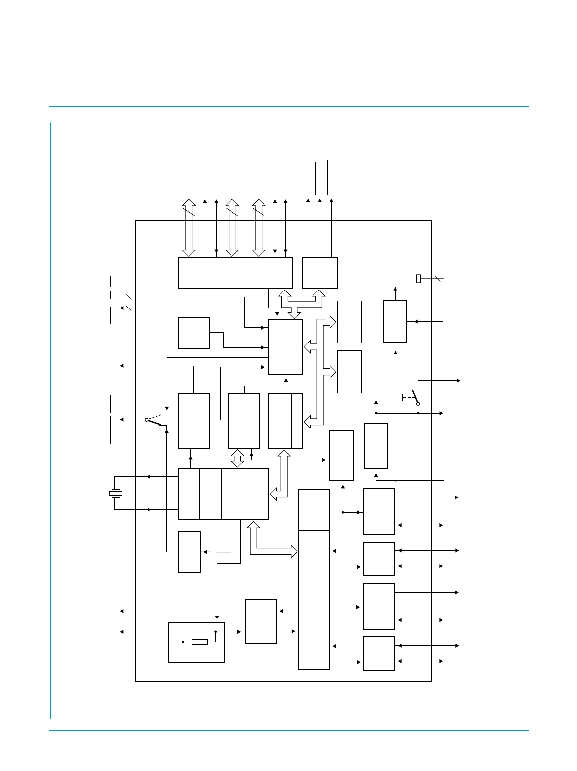
Fig 1. Block diagram of ISP1130.
Page 4
Philips Semiconductors
5. Pinning information
5.1 Pinning
ISP1130
USB compound hub with keyboard controller
handbook, halfpage
V
DN1_DM
DN1_DP
DN2_DM
DN2_DP
OC1/DPGL1
OC2/DPGL2
MX3/SCL
MX4/SDA
XTAL1
XTAL2
RESET
V
CC
GND
pu(3.3)
UP_DM
UP_DP
PSW1
PSW2
GND
MX0
MX1
MX2
MX5
MX6
MX7
MY0
MY1
MY2
1
2
3
4
5
6
7
8
9
10
11
12
13
14
15
16
17
18
19
20
21
22
23
24
25
26
27
28
ISP1130DL
MGS810
56
GND
55
CAPSLOCK
54
NUMLOCK
53
SCRLOCK
52
INT
51
PSEN
50
ALE
49
EA
SYNCLK
48
47
MEMSEL/UPGL
GND
46
45
MY17/WR
MY16/RD
44
MY15
43
MY14
42
MY13
41
MY12
40
MY11
39
MY10
38
MY9
37
MY8
36
MY7
35
MY6
34
MY5
33
MY4
32
MY3
31
V
30
reg(3.3)
GND
29
handbook, halfpage
OC1/DPGL1
OC2/DPGL2
MX4/SDA
XTAL1
XTAL2
RESET
V
CC
GND
V
pu(3.3)
UP_DM
UP_DP
DN1_DM
DN1_DP
DN2_DM
DN2_DP
PSW1
PSW2
GND
MX0
MX1
MX2
MX3/SCL
MX5
MX6
MX7
MY0
MY1
MY2
1
2
3
4
5
6
7
8
9
10
11
12
13
14
15
16
17
18
19
20
21
22
23
24
25
26
27
28
ISP1130N
MGS798
56
GND
55
CAPSLOCK
NUMLOCK
54
53
SCRLOCK
52
INT
PSEN
51
50
ALE
49
EA
SYNCLK
48
47
MEMSEL/UPGL
GND
46
45
MY17/WR
MY16/RD
44
MY15
43
MY14
42
MY13
41
MY12
40
MY11
39
MY10
38
MY9
37
MY8
36
MY7
35
MY6
34
MY5
33
MY4
32
MY3
31
V
30
reg(3.3)
GND
29
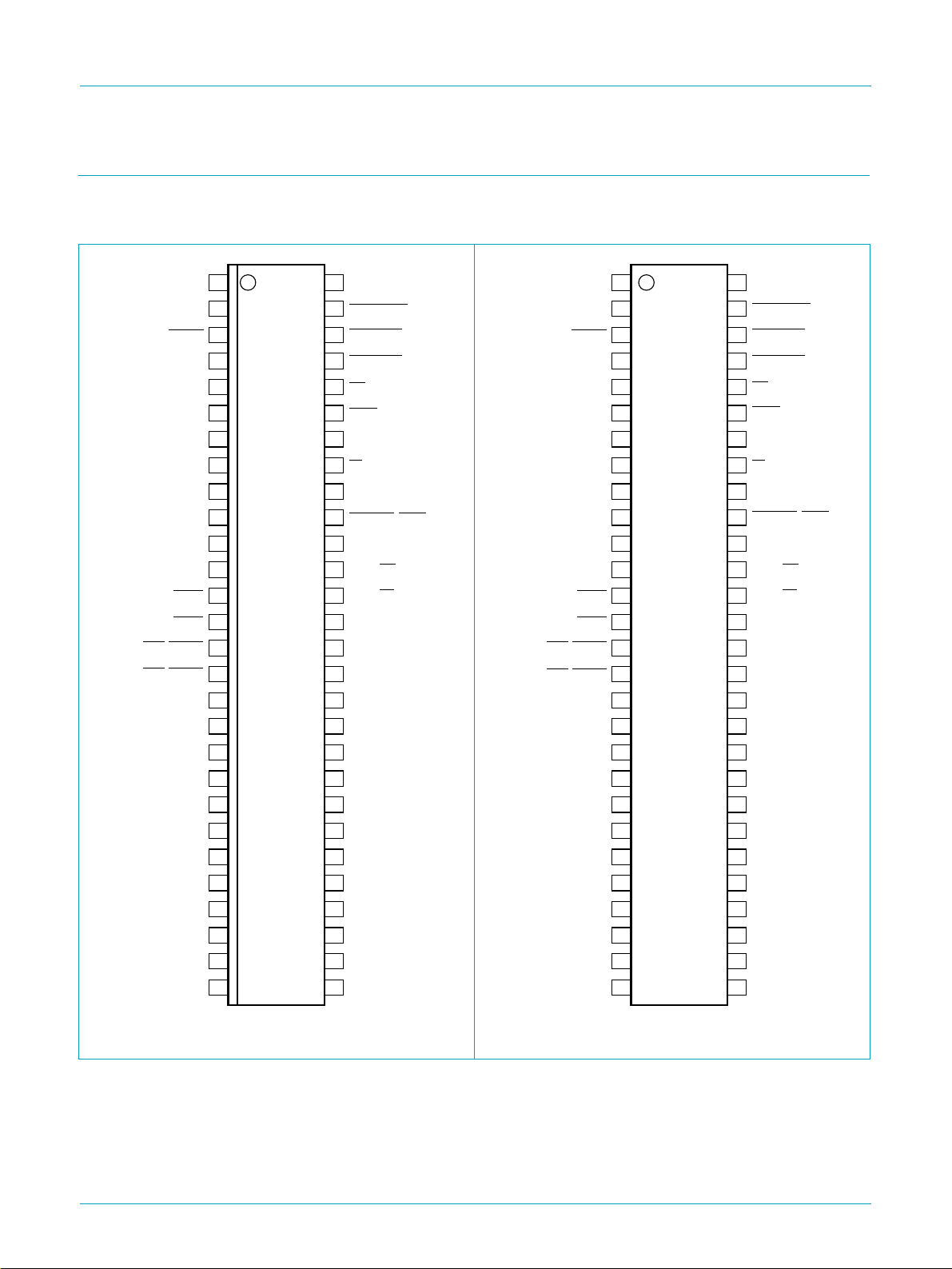
Fig 2. Pin configuration SSOP56. Fig 3. Pin configuration SDIP56.
9397 750 06895
Objective specification Rev. 01 — 23 March 2000 4 of 68
© Philips Electronics N.V. 2000. All rights reserved.
Page 5

Philips Semiconductors
5.2 Pin description
Table 2: Pin description (SSOP56 and SDIP56)
Symbol
XTAL1 1 I crystal oscillator input (6 MHz)
XTAL2 2 O crystal oscillator output (6 MHz)
RESET 3 I reset input (Schmitt trigger); a LOW level produces an
V
CC
GND 5 - ground supply
V
pu(3.3)
UP_DM 7 AI/O upstream port D− connection (analog)
UP_DP 8 AI/O upstream port D+ connection (analog)
DN1_DM 9 AI/O downstream port 1 D− connection (analog)
DN1_DP 10 AI/O downstream port 1 D+ connection (analog)
DN2_DM 11 AI/O downstream port 2 D− connection (analog)
DN2_DP 12 AI/O downstream port 2 D+ connection (analog)
PSW1 13 O power switch control output for downstream port 1
PSW2 14 O power switch control output for downstream port 2
OC1/DPGL1 15 AI/O pin function is controlled via the USBCON register (see
OC2/DPGL2 16 AI/O pin function is controlled via the USBCON register (see
GND 17 - ground supply
MX0 18 I keyboard matrix return line (5 V tolerant, open drain)
MX1 19 I keyboard matrix return line (5 V tolerant, open drain)
[1]
ISP1130
USB compound hub with keyboard controller
Pin Type Description
asynchronous reset; connect to V
(internal POR circuit)
4 - supply voltage; connect to USB supply V
6 - regulated supply voltage (3.3 V ± 10%) from internal
regulator; used to connect pull-up resistor on UP_DP line;
pin function is controlled via the Device Status Register
(see Table 36):
Connect = 0 — V
Connect = 1 — V
floating (high impedance)
pu(3.3)
= 3.3 V
pu(3.3)
(open-drain)
(open-drain)
Table 53):
EnableOverCurrent = 0 — GoodLink LEDindicator output
for downstream port 1 (analog, open-drain); to connect an
LED use a 330 Ω series resistor
EnableOverCurrent = 1 — overcurrent sense input for
downstream port 1 (analog or digital); overcurrent sensing
can be either analog (AnalogOCDisable = 0) or digital
(AnalogOCDisable = 1)
Table 53):
EnableOverCurrent = 0 — GoodLink LEDindicator output
for downstream port 2 (analog, open-drain); to connect an
LED use a 330 Ω series resistor
EnableOverCurrent = 1 — overcurrent sense input for
downstream port 2 (analog or digital); overcurrent sensing
can be either analog (AnalogOCDIsable = 0) or digital
(AnalogOCDisable = 1)
for power-on reset
CC
BUS
[2]
[2]
9397 750 06895
Objective specification Rev. 01 — 23 March 2000 5 of 68
© Philips Electronics N.V. 2000. All rights reserved.
Page 6

Philips Semiconductors
ISP1130
USB compound hub with keyboard controller
Table 2: Pin description (SSOP56 and SDIP56)
Symbol
[1]
Pin Type Description
…continued
MX2 20 I keyboard matrix return line (5 V tolerant, open drain)
MX3/SCL 21 I/O pin function is controlled via the I2C0CON register (see
Table 76):
ENS1 = 0 — keyboard matrix return line (5 V tolerant,
open drain)
[2]
ENS1 = 1 — I2C-bus clock output (5 V tolerant, open
[2]
drain)
MX4/SDA 22 I/O pin function is controlled via the I2C0CON register (see
Table 76):
ENS1 = 0 — keyboard matrix return line (5 V tolerant,
open drain)
[2]
ENS1 = 1 — bidirectional I2C-bus data line (5 V tolerant,
open drain)
MX5 23 I keyboard matrix return line(5 V tolerant, open drain)
[2]
[2]
MX6 24 I keyboard matrix return line (5 V tolerant, open drain)
MX7 25 I keyboard matrix return line (5 V tolerant, open drain)
MY0 26 I/O bidirectional keyboard matrix scan line (5 V tolerant)
MY1 27 I/O bidirectional keyboard matrix scan line (5 V tolerant)
MY2 28 I/O bidirectional keyboard matrix scan line (5 V tolerant)
GND 29 - ground supply
V
reg(3.3)
30 - regulated supply voltage (3.3 V ± 10%) from internal
regulator; used to supply external devices
MY3 31 I/O bidirectional keyboard matrix scan line (5 V tolerant)
MY4 32 I/O bidirectional keyboard matrix scan line (5 V tolerant)
MY5 33 I/O bidirectional keyboard matrix scan line (5 V tolerant)
MY6 34 I/O bidirectional keyboard matrix scan line (5 V tolerant)
MY7 35 I/O bidirectional keyboard matrix scan line (5 V tolerant)
MY8 36 I/O bidirectional keyboard matrix scan line (5 V tolerant)
MY9 37 I/O bidirectional keyboard matrix scan line (5 V tolerant)
MY10 38 I/O bidirectional keyboard matrix scan line (5 V tolerant)
MY11 39 I/O bidirectional keyboard matrix scan line (5 V tolerant)
MY12 40 I/O bidirectional keyboard matrix scan line (5 V tolerant)
MY13 41 I/O bidirectional keyboard matrix scan line (5 V tolerant)
MY14 42 I/O bidirectional keyboard matrix scan line (5 V tolerant)
MY15 43 I/O bidirectional keyboard matrix scan line (5 V tolerant)
MY16/RD 44 I/O bidirectional keyboard matrix scan line (5 V tolerant)
used as read strobe when accessing external memory
WR 45 I/O bidirectional keyboard matrix scan line (5 V tolerant)
MY17/
used as write strobe when accessing external memory
GND 46 - ground supply
[2]
[2]
[2]
[3]
[3]
[3]
[3]
[3]
[3]
[3]
[3]
[3]
[3]
[3]
[3]
[3]
[3]
[3]
[3]
[3]
;
[3]
;
9397 750 06895
Objective specification Rev. 01 — 23 March 2000 6 of 68
© Philips Electronics N.V. 2000. All rights reserved.
Page 7

Philips Semiconductors
ISP1130
USB compound hub with keyboard controller
Table 2: Pin description (SSOP56 and SDIP56)
Symbol
MEMSEL/
UPGL
SYNCLK 48 O embedded microcontroller clock output; used for emulation
EA 49 I External Address enable input (internal pull-up); used to
ALE 50 O Address Latch Enable output; used to demultiplex AD0
PSEN 51 O Program Store ENable output; selects external memory for
INT 52 I external interrupt input (edge-triggered)
SCRLOCK 53 O control output for Scroll Lock LED (open-drain)
NUMLOCK 54 O control output for Num Lock LED (open-drain)
CAPSLOCK 55 O control output for Caps Lock LED (open-drain)
GND 56 - ground supply
[1] Symbol names with an overscore (e.g. NAME) indicate active LOW signals.
[2] MXn pins have an internal 8.2 kΩ pull-up resistor.
[3] MYn pins have an internal 82 kΩ pull-down resistor (keyboard matrix enabled) or an internal 8.2 kΩ
[1]
pull-up resistor (keyboardmatrix disabled).This is controlled by bit DisableKBDMatrix in the USBCON
register, see Table 53.
Pin Type Description
47 O pin function is controlled via the USBCON register (see
Table 53):
GL-MEMSELSelection = 0 — upstream port GoodLink
indicator output (open-drain)
GL-MEMSELSelection = 1 — chip select output for
external serial EEPROM (open-drain)
access external memory
during external memory access
program execution
…continued
6. Functional description
The ISP1130 is a compound USB hub with an integrated keyboard controller.It has 2
bus-powered downstream ports with 3 non-removable embedded functions, the first
of which is dedicated to the keyboard function. The downstream ports can be used to
connect low-speed or full-speed USB peripherals, such as a mouse, printer, another
keyboard or another hub. The block diagram is shown in Figure 1.
The embedded functions have no external hardware connections. They provide USB
endpoints for equipment functions implemented by a microcontroller. Each endpoint
has an associated FIFO buffer in the on-board RAM, which can be accessed by the
integrated microcontroller via memory mapped registers using special commands
(see Section 9).
An optional serial I2C-bus interface (see Section 11) is provided for external
EEPROM access, allowing the user to program the vendor ID, product ID or activate
the built-in keyboard matrix.
9397 750 06895
Objective specification Rev. 01 — 23 March 2000 7 of 68
© Philips Electronics N.V. 2000. All rights reserved.
Page 8

Philips Semiconductors
6.1 80C51 microcontroller
An integrated 80C51 microcontroller serves as a keyboard controller. It has 8 kbytes
of mask ROM and 256 bytes of RAM. The I/O ports have been configured as an
8 × 18 line scan matrix. Three LED control outputs are available for keyboard status
indicators (Caps Lock, Num Lock and Scroll Lock). Interfacingto the USB hub is done
via 3 registers (command, data, status), which are accessible via the external data
memory address space (MOVX instruction).
The keyboard firmware resides in the ROM and enumerates the embedded function
as ‘HID compatible keyboard device’ during hub initialization.
The microcontroller runs on a 12 MHz clock, derived from the PLL oscillator. A
watchdog timer resets the microcontroller in case of a software hang-up.
6.2 Analog transceivers
The integrated transceivers interface directly to the USB cables through external
termination resistors. They are capable of transmitting and receiving serial data at
both ‘full-speed’ (12 Mbit/s) and ‘low-speed’ (1.5 Mbit/s) data rates. The slew rates
are adjusted according to the speed of the device connected and lie within the range
mentioned in the
USB compound hub with keyboard controller
USB Specification Rev. 1.1
ISP1130
.
6.3 Philips Serial Interface Engine (SIE)
The Philips SIE implements the full USB protocol layer. It is completely hardwired for
speed and needs no firmware intervention. The functions of this block include:
synchronization pattern recognition, parallel/serial conversion, bit (de-)stuffing, CRC
checking/generation, Packet IDentifier (PID) verification/generation, address
recognition, handshake evaluation/generation.
6.4 Hub repeater
The hub repeater is responsible for managing connectivity on a ‘per packet’ basis. It
implements ‘packet signalling’ and ‘resume’ connectivity. Low-speed devices can be
connected to downstream ports. If a low-speed device is detected the repeater will
not propagate upstream packetsto the corresponding port, unless they are preceded
by a PREAMBLE PID.
6.5 End-of-frame timers
This block contains the specified EOF1 and EOF2 timers which are used to detect
‘loss-of-activity’ and ‘babble’ error conditions in the hub repeater. The timers also
maintain the low-speed keep-alive strobe which is sent at the beginning of a frame.
6.6 General and individual port controller
The general and individual port controllers together provide status and control of
individual downstream ports. Any port status change will be reported to the host via
the hub status change (interrupt) endpoint.
9397 750 06895
Objective specification Rev. 01 — 23 March 2000 8 of 68
© Philips Electronics N.V. 2000. All rights reserved.
Page 9
Philips Semiconductors
6.7 GoodLink
Indication of a good USB connection is provided through GoodLink technology. An
LED can be directly connected via an external 330 Ω resistor. The ISP1130 supports
GoodLink indication for the hub (upstream port) via output MEMSEL/UPGL and for
the two downstream ports via OCn/DPGLn, controlled via bits GL-MEMSELSelection
and EnableOverCurrent in the USBCON register (see Table 53).
During enumeration the LED blinks on momentarily. After successful configuration of
the ISP1130, the LED is permanently on. The hub GoodLink indicator blinks off for
approximately 128 ms when the hub receives a packet addressed to it. Downstream
GoodLink indicators blink upon an acknowledgment from the associated port. In
‘suspend’ mode the LED is off.
This feature provides a user-friendly indication of the status of the hub, the connected
downstream devices and the USB traffic. It is a useful diagnostics tool to isolate faulty
USB equipment and helps to reduce field support and hotline costs.
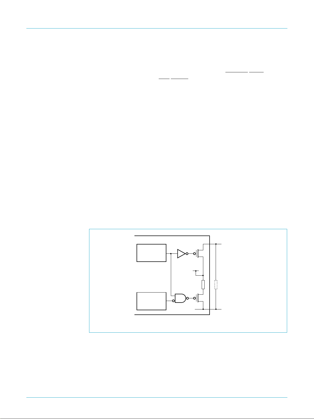
6.8 SoftConnect
The connection to the USB is accomplished by bringing D+ (for full-speed USB
devices) HIGH through a 1.5 kΩ pull-up resistor. In the ISP1130, the 1.5 kΩ pull-up
resistor is integrated on-chip and by default is disconnected from the +3.3 V supply.
ISP1130
USB compound hub with keyboard controller
The integrated microcontroller controls the connection of the internal resistor on D+ to
V
the Device Status register switches on V
via bit SoftConnect_N in the USBCON register (see Table 53). Bit Connect in
pu(3.3)
(defaultis off) to an alternative external
pu(3.3)
pull-up resistor. A functional schematic diagram is given in Figure 4.
dth
Connect
(Device Status
Register)
SoftConnect_N
(Configuration
Register)
Fig 4. SoftConnect control logic.
ISP1130
3.3 V
supply
1.5 kΩ
(internal
pull-up)
MGL920
V
pu(3.3)
1.5 kΩ
(external
pull-up)
UP_DP
This mechanism allows the microcontroller to complete its initialization sequence
before deciding to establish connection to the USB. Re-initialization of the USB
connection can also be performed without disconnecting the cable.
It should be noted that the tolerance of the internal resistors is higher (30%) than is
specified by the USB specification (5%). However, the overall VSE voltage
specification for the connection can still be met with good margin (see Table 92). The
decision to use this feature lies with the USB equipment designer.
9397 750 06895
Objective specification Rev. 01 — 23 March 2000 9 of 68
© Philips Electronics N.V. 2000. All rights reserved.
Page 10

Philips Semiconductors
6.9 Bit clock recovery
The bit clock recovery circuit recovers the clock from the incoming USB data stream
using a 4× oversampling principle. It is able to track jitter and frequency drift as
specified by the
6.10 Voltage regulator
A 5 to 3.3 V DC-DC regulator is integrated on-chip to supply the analog transceiver
and internal logic. This can also be used to supply the terminal 1.5 kΩ pull-up resistor
on the D+ line of the upstream connection.
6.11 PLL clock multiplier
A 6 to 48 MHz clock multiplier Phase-Locked Loop (PLL) is integrated on-chip. This
allows for the use of low-cost 6 MHz crystals. The low crystal frequency also
minimizes Electro-Magnetic Interference (EMI). The PLL requires no external
components.
6.12 Overcurrent detection
USB compound hub with keyboard controller
USB Specification Rev. 1.1
ISP1130
.
An overcurrent detection circuit for downstream ports has been integrated on-chip. It
is self-reporting, resets automatically, has a low trip time and requires no external
components. The ISP1130 supports individual overcurrent detection.
6.13 Power-on reset
The ISP1130 has an internal power-on reset circuit, which generates a reset pulse
when the supply voltage is switched on and when the supply voltage drops below a
predetermined threshold value (see Table 89).
6.14 I2C-bus interface
A serial I2C-bus interface (single master or slave, bit rate up to 400 kHz) is provided
to read vendor ID,product ID and other configuration data from an external EEPROM
(e.g., Philips PCF8582 or equivalent). For more information, see Section 11.
The I2C-bus interface timing is programmable and complies with the standard mode
and the Fast mode of operation as described in
number 9398 393 40011.
The I2C-bus and how to use it
, order
9397 750 06895
Objective specification Rev. 01 — 23 March 2000 10 of 68
© Philips Electronics N.V. 2000. All rights reserved.
Page 11

Philips Semiconductors
7. Endpoint descriptions
Each USB device is logically composed of several independent endpoints. An
endpoint acts as a terminus of a communication flow between the host and the
device. At design time each endpoint is assigned a unique number (endpoint
identifier, see Table 3). The combination of the device address (given by the host
during enumeration), the endpoint number and the transfer direction allows each
endpoint to be uniquely referenced.
7.1 Endpoint configuration
The ISP1130 hub has 1 to 2 downstream ports and 1 to 3 embedded functions. The
upstream and downstream ports are fully handled by hardware and require no
firmware intervention. Downstream port 2 can be disabled by connecting both D+ and
D− to VCC.
The number of embedded functions can be configured from 1 to 3 via the USBCONA
register. These embedded functions give access to the keyboardcontroller and other
optional software functions. The functions are assigned as follows:
ISP1130
USB compound hub with keyboard controller
Embedded function 1: standard keyboard
•
Embedded function 2:
•
– multimedia functions (e.g. volume control)
– ACPI system control
– application launch keys
Embedded function 3: user-defined functions.
•
Each embedded function has two endpoint types: endpoint 0 (control) and endpoint 1
(generic: bulk and/or interrupt). The embedded function endpoints can handle a
maximum of 8 bytes per transfer.
Table 3: Endpoint allocation
Function Ports Endpoint
0: upstream
Hub
Embedded
Function 1
Embedded
Function 2
[4]
1, 2
:
downstream
3 (or 2
4 (or 3
identifier
0 control -
1 interrupt -
[5]
) 0 control 0 OUT 8
1 generic
[5]
) 0 control 4 OUT 8
1 generic
Transfer
type
Endpoint
index
[2]
[2]
-
[2]
1IN8
[3]
2 OUT 8
3IN8
5IN8
[3]
6 OUT 8
7IN8
Direction
OUT 64
IN 64
IN 1
[1]
Max. packet
size (bytes)
9397 750 06895
Objective specification Rev. 01 — 23 March 2000 11 of 68
© Philips Electronics N.V. 2000. All rights reserved.
Page 12

Philips Semiconductors
ISP1130
USB compound hub with keyboard controller
Table 3: Endpoint allocation
Function Ports Endpoint
Embedded
Function 3
[1] IN: input for the USB host; OUT: output from the USB host.
[2] Hub endpoints are not indexed.
[3] Generic endpoint can be used as bulk or interrupt endpoint.
[4] Port 2 can be disabled by connecting both D+ and D− to VCC.
[5] The port number is reduced by 1 when downstream port 2 is disabled.
5 (or 4
[5]
) 0 control 8 OUT 8
…continued
identifier
1 generic
Transfer
type
Endpoint
index
9IN8
[3]
10 OUT 8
11 IN 8
Direction
[1]
7.2 Hub endpoint 0 (control)
All USB devices and functions must implement a default control endpoint (ID = 0).
This endpoint is used by the host to configure the device and to perform generic USB
status and control access.
The ISP1130 hub supports the following USB descriptor information through its
control endpoint 0, which can handle transfers of 64 bytes maximum:
Device descriptor
•
Configuration descriptor
•
Interface descriptor
•
Endpoint descriptor
•
Hub descriptor
•
String descriptor.
•
Max. packet
size (bytes)
7.3 Hub endpoint 1 (interrupt)
Endpoint 1 is used by the ISP1130 hub to provide port status change information to
the host. This endpoint can be accessed only after the hub has been configured by
the host (by sending the Set Configuration command).
Endpoint 1 is an interrupt endpoint: the host polls it once every 255 ms by sending an
IN token. If the hub has detected no change in the port status it returns a NAK (Not
AcKnowledge) response to this request, otherwise it sends the Status Change byte
(see Table 4).
Table 4: Status Change byte: bit allocation
Bit Symbol Description
0 Hub SC a logic 1 indicates a status change on the hub’s upstream port
1 Port 1 SC a logic 1 indicates a status change on downstream port 1
2 Port 2 SC a logic 1 indicates a status change on downstream port 2 or on
embedded function 1 (downstream port 2 disabled)
3 Port 3 SC a logic 1 indicates a status change on embedded function 1 or on
embedded function 2 (downstream port 2 disabled)
9397 750 06895
Objective specification Rev. 01 — 23 March 2000 12 of 68
© Philips Electronics N.V. 2000. All rights reserved.
Page 13

Philips Semiconductors
ISP1130
USB compound hub with keyboard controller
8. Host requests
8.1 Standard requests
Table 4: Status Change byte: bit allocation
Bit Symbol Description
4 Port 4 SC a logic 1 indicates a status change on embedded function 2 or on
embedded function 3 (downstream port 2 disabled)
5 Port 5 SC a logic 1 indicates a status change on embedded function 3; not used
if downstream port 2 is disabled
6 reserved not used
7 reserved not used
…continued
The ISP1130 handles all standard USB requests from the host via control endpoint 0.
The control endpoint can handle a maximum of 64 bytes per transfer.
Remark: Please note that the USB data transmission order is Least Significant Bit
(LSB) first. In the following tables multi-byte variables are displayed least significant
byte first.
Table 5 shows the supported standard USB requests. Some requests are explicitly
unsupported. All other requests will be responded with a STALL packet.
Table 5: Standard USB requests
Request name bmRequestType
Address
Set Address X000 0000 05 address
Configuration
Get Configuration 1000 0000 08 00, 00 00, 00 01, 00 configuration
Set Configuration (0) X000 0000 09 00, 00 00, 00 00, 00 none
Set Configuration (1) X000 0000 09 01, 00 00, 00 00, 00 none
Descriptor
Get Configuration
Descriptor
Get Device Descriptor 1000 0000 06 00, 01 00, 00 length
Get String Descriptor (0) 1000 0000 06 00, 03 00, 00 length
Get String Descriptor (1) 1000 0000 06 01, 03 09, 04 length
Get String Descriptor (2) 1000 0000 06 02, 03 09, 04 length
byte 0 [7:0]
(Bin)
1000 0000 06 00, 02 00, 00 length
bRequest
byte 1
(Hex)
wValue
byte 2, 3
(Hex)
wIndex
byte 4, 5
(Hex)
[1]
00, 00 00, 00 none
wLength
byte 6, 7
(Hex)
Data
value = 01H
[2]
[2]
[2]
[2]
[2]
configuration,
interface and
endpoint
descriptors
device
descriptor
language ID
string
manufacturer
string
product string
9397 750 06895
Objective specification Rev. 01 — 23 March 2000 13 of 68
© Philips Electronics N.V. 2000. All rights reserved.
Page 14

Philips Semiconductors
ISP1130
USB compound hub with keyboard controller
Table 5: Standard USB requests
Request name bmRequestType
byte 0 [7:0]
(Bin)
…continued
bRequest
byte 1
(Hex)
wValue
byte 2, 3
(Hex)
wIndex
byte 4, 5
(Hex)
wLength
byte 6, 7
(Hex)
Data
Feature
Clear Device Feature
X000 0000 01 01, 00 00, 00 00, 00 none
(REMOTE_WAKEUP)
Clear Endpoint (1)
X000 0010 01 00, 00 81, 00 00, 00 none
Feature (HALT/STALL)
Set Device Feature
X000 0000 03 01, 00 00, 00 00, 00 none
(REMOTE_WAKEUP)
Set Endpoint (1)
X000 0010 03 00, 00 81, 00 00, 00 none
Feature (HALT/STALL)
Status
Get Device Status 1000 0000 00 00, 00 00, 00 02, 00 device status
Get Interface Status 1000 0001 00 00, 00 00, 00 02, 00 zero
Get Endpoint (0) Status 1000 0010 00 00, 00 00/80
[3]
, 00 02, 00 endpoint 0
status
Get Endpoint (1) Status 1000 0010 00 00, 00 81, 00 02, 00 endpoint 1
status
Unsupported
Set Descriptor 0000 0000 07 XX, XX XX, XX XX, XX descriptor;
STALL
Get Interface 1000 0001 0A 00, 00 XX, XX 01, 00 STALL
Set Interface X000 0001 0B XX, XX XX, XX 00, 00 STALL
Synch Frame 1000 0010 0C 00, 00 XX, XX 02, 00 STALL
[1] Device address: 0 to 127.
[2] Returned value in bytes.
[3] MSB specifies endpoint direction: 0 = OUT, 1= IN. The ISP1130 accepts either value.
8.2 Hub specific requests
In Table 6 the supported hub specific requests are listed, as well as some
unsupported requests. Table 7 provides the feature selectors for setting or clearing
port features.
Table 6: Hub specific requests
Request name bmRequestType
byte 0 [7:0]
(Bin)
Descriptor
Get Hub Descriptor 1010 0000 06 00, 00/29
Feature
Clear Hub Feature
X010 0000 01 00, 00 00, 00 00, 00 none
(C_LOCAL_POWER)
Clear Port Feature
X010 0011 01 feature
(feature selectors)
Set Port Feature
X010 0011 03 feature
(feature selectors)
bRequest
byte 1
(Hex)
wValue
byte 2, 3
(Hex)
wIndex
byte 4, 5
(Hex)
[1]
00, 00 length
[3]
, 00 port
[3]
, 00 port
wLength
byte 6, 7
(Hex)
[2]
, 00 hub descriptor
[4]
, 00 00, 00 none
[4]
, 00 00, 00 none
Data
9397 750 06895
Objective specification Rev. 01 — 23 March 2000 14 of 68
© Philips Electronics N.V. 2000. All rights reserved.
Page 15

Philips Semiconductors
ISP1130
USB compound hub with keyboard controller
Table 6: Hub specific requests
Request name bmRequestType
…continued
byte 0 [7:0]
(Bin)
bRequest
byte 1
(Hex)
wValue
byte 2, 3
(Hex)
wIndex
byte 4, 5
(Hex)
wLength
byte 6, 7
(Hex)
Data
Status
Get Hub Status 1010 0000 00 00, 00 00, 00 04, 00 hubstatusand
status change
field
[4]
Get Port Status 1010 0011 00 00, 00 port
, 00 04, 00 port status
Unsupported
[4]
Get Bus Status 1010 0011 02 00, 00 port
Clear Hub Feature
X010 0000 01 01, 00 00, 00 00, 00 STALL
, 00 01, 00 STALL
(C_OVER_CURRENT)
Set Hub Descriptor X010 0000 07 XX, XX 00, 00 3E, 00 STALL
Set Hub Feature
X010 0000 03 00, 00 00, 00 00, 00 STALL
(C_LOCAL_POWER)
Set Hub Feature
X010 0000 03 01, 00 00, 00 00, 00 STALL
(C_OVER_CURRENT)
[1]
USB Specification Rev. 1.0
[2] Returned value in bytes.
[3] Feature selector value, see Table 7.
[4] Downstream port identifier: 1 to 5 (1, 2: downstream ports, 3 to 5: embedded functions 1 to 3). If downstream port 2 is disabled, the port
identifiers are 1 to 4 (1: downstream port, 2 to 4: embedded functions 1 to 3).
uses 00H,
USB Specification Rev. 1.1
specifies 29H.
Table 7: Port feature selectors
Feature selector name Value (Hex) Set feature Clear feature
PORT_CONNECTION 00 not used not used
PORT_ENABLE 01 not used disables a port
PORT_SUSPEND 02 suspends a port resumes a port
PORT_OVERCURRENT 03 not used not used
PORT_RESET 04 resets and enables
not used
a port
PORT_POWER 08 powers on a port powers off a port
PORT_LOW_SPEED 09 not used not used
C_PORT_CONNECTION 10 not used clears port connection
change bit
C_PORT_ENABLE 11 not used clears port enable
change bit
C_PORT_SUSPEND 12 not used clears port suspend
change bit
C_PORT_OVERCURRENT 13 not used clears port overcurrent
change bit
C_PORT_RESET 14 not used clears port reset
change bit
9397 750 06895
Objective specification Rev. 01 — 23 March 2000 15 of 68
© Philips Electronics N.V. 2000. All rights reserved.
Page 16

Philips Semiconductors
8.3 Descriptors
The ISP1130 hub controller supports the following standard USB descriptors:
•
•
•
•
•
•
Table 8: Device descriptor
Values in square brackets are optional.
Offset
(bytes)
0 bLength 1 12 descriptor length = 18 bytes
1 bDescriptorType 1 01 type = DEVICE
2 bcdUSB 2 10, 01
4 bDeviceClass 1 09 HUB_CLASSCODE
5 bDeviceSubClass 1 00 6 bDeviceProtocol 1 00 7 bMaxPacketSize0 1 40 packet size = 64 bytes
8 idVendor 2 VID vendor ID; programmable via the Set
10 idProduct 2 PID product ID; programmable via the Set
12 bcdDevice 2 00,
14 iManufacturer 1 00 no manufacturer string (default)
15 iProduct 1 00 no product string (default)
16 iSerialNumber 1 00 no serial number string
17 bNumConfigurations 1 01 one configuration
Device
Configuration
Interface
Endpoint
Hub
String.
Field name Size
ISP1130
USB compound hub with keyboard controller
(bytes)
Value
(Hex)
XX
[01] manufacturer string enabled
[02] product string enabled
Comments
USB Specification Rev. 1.1
VID/PID command (see Table 43)
VID/PID command (see Table 43)
device release 1.0 (XX = 01H); silicon
[1]
revision increments this value
[2]
[2]
[1] XX represents the hardware setting DEVREV, which indicates the 8-bit device release number. This
value is incremented upon silicon revision.
[2] Controlled via bit StringDescriptorEnable in the Set Mode command (see Table 25).
Table 9: Configuration descriptor
Values in square brackets are optional.
Offset
(bytes)
0 bLength 1 09 descriptor length=9bytes
1 bDescriptorType 1 02 type = CONFIGURATION
2 wTotalLength 2 19, 00 total length of configuration, interface
4 bNumInterfaces 1 01 one interface
9397 750 06895
Objective specification Rev. 01 — 23 March 2000 16 of 68
Field name Size
(bytes)
Value
(Hex)
Comments
and endpoint descriptors (25 bytes)
© Philips Electronics N.V. 2000. All rights reserved.
Page 17

Philips Semiconductors
ISP1130
USB compound hub with keyboard controller
Table 9: Configuration descriptor
…continued
Values in square brackets are optional.
Offset
(bytes)
Field name Size
(bytes)
Value
(Hex)
Comments
5 bConfigurationValue 1 01 configuration value = 1
6 iConfiguration 1 00 no configuration string
7 bmAttributes 1 A0 bus-powered with remote wake-up
(default)
[E0] hybrid-powered with remote wake-up;
configured via bit 7 in the USBCON
register (see Table 53)
8 MaxPower
[1] Value in units of 2 mA.
[1]
1 32 100 mA
Table 10: Interface descriptor
Offset
(bytes)
Field name Size
(bytes)
Value
(Hex)
Comments
0 bLength 1 09 descriptor length=9bytes
1 bDescriptorType 1 04 type = INTERFACE
2 bInterfaceNumber 1 00 3 bAlternateSetting 1 00 no alternate setting
4 bNumEndpoints 1 01 status change (interrupt) endpoint
5 bInterfaceClass 1 09 HUB_CLASSCODE
6 bInterfaceSubClass 1 00 7 bInterfaceProtocol 1 00 no class-specific protocol
8 bInterface 1 00 no interface string
Table 11: Endpoint descriptor
Offset
(bytes)
Field name Size
(bytes)
Value
(Hex)
Comments
0 bLength 1 07 descriptor length=7bytes
1 bDescriptorType 1 05 type = ENDPOINT
2 bEndpointAddress 1 81 endpoint 1, direction: IN
3 bmAttributes 1 03 interrupt endpoint
4 wMaxPacketSize 2 01, 00 packet size = 1 byte
6 bInterval 1 FF polling interval (255 ms)
Table 12: Hub descriptor
Offset
(bytes)
Field name Size
(bytes)
Value
(Hex)
Comments
0 bDescLength 1 09 descriptor length=9bytes
1 bDescriptorType 1 29 type = HUB
[2]
2 bNbrPorts 1 03
number of downstream ports (1 or 2;
default = 2) + number of embedded
functions (1 to 3; default = 1)
9397 750 06895
Objective specification Rev. 01 — 23 March 2000 17 of 68
© Philips Electronics N.V. 2000. All rights reserved.
Page 18

Philips Semiconductors
ISP1130
USB compound hub with keyboard controller
Table 12: Hub descriptor
Offset
Field name Size
(bytes)
…continued
(bytes)
Value
(Hex)
Comments
3 wHubCharacteristics 2 0D, 00 individual power switching,
individual overcurrent protection
15, 00 individual power switching,
no overcurrent protection
[1]
5 bPwrOn2PwrGood
1 32 100 ms
6 bHubContrCurrent 1 64 maximum hub controller current
(100 mA)
[3]
7 DeviceRemovable 1 08
downstream ports removable;
embedded functions non-removable
8 PortPwrCtrlMask 1 FF must be all ones for compatibility with
USB Specification Rev. 1.0
[1] Value in units of 2 ms.
[2] Depending on the number of embedded functions configured, the value ranges from 03H to 05H or
from 02H to 04H (downstream port 2 disabled).
Remark: Downstream port 2 can be disabled by connecting both D+ and D− to VCC. Embedded
functions are configured via the USBCONA register (see Table 55).
[3] Default value (08H): ports 1 and 2 removable, port 3 non-removable. The value can be 08H, 18H or
38H depending on the configured number of embedded functions (1, 2 or 3). When downstream
port 2 is disabled, the possible values are 4CH, 0CH or 1CH (1, 2 or 3 embedded functions).
Table 13: String descriptors
String descriptors are optional and therefore disabled by default; they can be enabled via the
Set Mode command (see Table 25).
Offset
(bytes)
Field name Size
(bytes)
Value
(Hex)
Comments
String descriptor (0): language ID string
0 bLength 1 04 descriptor length=4bytes
1 bDescriptorType 1 03 type = STRING
2 bString 2 09, 04 LANGID code zero
String descriptor (1): manufacturer string
0 bLength 1 2E descriptor length = 46 bytes
1 bDescriptorType 1 03 type = STRING
[1]
2 bString 44 UC
“Philips Semiconductors”
String descriptor (2): product string
0 bLength 1 10 descriptor length = 16 bytes
1 bDescriptorType 1 03 type = STRING
[1]
2 bString 14 UC
[1] Unicode encoded string.
[2] X represents the hardware setting DEVNAME (4 bits), which specifies the final digit (X) in the device
name string “ISP113X”. The Unicode representation of this digit is “0000.0000.0011.DEVNAME”.
“ISP113X”
[2]
; X = 0H for the ISP1130
9397 750 06895
Objective specification Rev. 01 — 23 March 2000 18 of 68
© Philips Electronics N.V. 2000. All rights reserved.
Page 19

Philips Semiconductors
8.4 Hub responses
This section describes the hub responses to requests from the USB host.
8.4.1 Get device status
The hub returns 2 bytes, see Table 14.
Table 14: Get device status response
Bit # Function Value Description
0 self-powered 0 bus-powered
1 remote wake-up 0 no remote wake-up
2 to 15 reserved 0 -
8.4.2 Get configuration
The hub returns 1 byte, see Table 15.
Table 15: Get configuration response
Bit # Function Value Description
0 configuration value 0 device not configured
1 to 7 reserved 0 -
ISP1130
USB compound hub with keyboard controller
1 hybrid-powered
1 remote wake-up enabled
1 device configured
8.4.3 Get interface status
The hub returns 2 bytes, see Table 16.
Table 16: Get interface status response
Bit # Function Value Description
0 to 15 reserved 0 -
8.4.4 Get hub status
The hub returns 4 bytes, see Table 17.
Table 17: Get hub status response
Bit # Function Value Description
0 local power source 0 local power supply good
1 overcurrent indicator 0 no overcurrent condition
2 to 15 reserved 0 16 local power status change 0 no change in local power status
17 overcurrent indicator change 0 no change in overcurrent condition
18 to 31 reserved 0 -
1 hub overcurrent condition detected
1 overcurrent condition changed
9397 750 06895
Objective specification Rev. 01 — 23 March 2000 19 of 68
© Philips Electronics N.V. 2000. All rights reserved.
Page 20

Philips Semiconductors
8.4.5 Get port status
The hub returns 4 bytes. The first 2 bytes contain the port status bits (wPortStatus,
see Table 18). The last 2 bytes hold the port status change bits (wPortChange, see
Table 19).
Table 18: Get port status response (wPortStatus)
Bit # Function Value Description
0 current connect status 0 no device present
1 port enabled/disabled 0 port disabled
2 suspend 0 port not suspended
3 overcurrent indicator 0 no overcurrent condition
4 reset 0 reset not asserted
5 to 7 reserved 0 8 port power 0 port powered off
9 low-speed device attached 0 full-speed device attached
10 to 15 reserved 0 -
ISP1130
USB compound hub with keyboard controller
1 device present on this port
1 port enabled
1 port suspended
1 overcurrent condition detected
1 reset asserted
1 port power on
1 low-speed device attached
Table 19: Get port status response (wPortChange)
Bit # Function Value Description
0 connect status change 0 no change in current connect status
1 port enabled/disabled
change
2 suspend change 0 no change in suspend status
3 overcurrent indicator change 0 no change in overcurrent status
4 reset change 0 no change in reset status
5 to 15 reserved 0 -
8.4.6 Get configuration descriptor
The hub returns 25 bytes containing the configuration descriptor (9 bytes, see
Table 9), the interface descriptor (9 bytes, see Table 10) and the endpoint descriptor
(7 bytes, see Table 11).
8.4.7 Get device descriptor
The hub returns 18 bytes containing the device descriptor, see Table 8.
1 current connect status changed
0 no port error
1 port disabled by a port error
1 resume complete
1 overcurrent indicator changed
1 reset complete
9397 750 06895
Objective specification Rev. 01 — 23 March 2000 20 of 68
© Philips Electronics N.V. 2000. All rights reserved.
Page 21

Philips Semiconductors
8.4.8 Get hub descriptor
The hub returns 9 bytes containing the hub descriptor, see Table 12.
8.4.9 Get string descriptor (0)
The hub returns 4 bytes containing the language ID, see Table 13.
8.4.10 Get string descriptor (1)
The hub returns 46 bytes containing the manufacturer name, see Table 13.
8.4.11 Get string descriptor (2)
The hub returns 16 bytes containing the product name, see Table 13.
ISP1130
USB compound hub with keyboard controller
9397 750 06895
Objective specification Rev. 01 — 23 March 2000 21 of 68
© Philips Electronics N.V. 2000. All rights reserved.
Page 22

Philips Semiconductors
9. Commands
There are three basic types of commands: Initialization, Data and General
commands. Respectively, these are used to initialize the hub and the embedded
functions; for data flow between the hub, embedded functions and the host; for
controlling individual downstream ports; and general hub operation.
The embedded microcontroller has access to the hub functions via 3 dedicated
control registers (Command, Data, Status), which are mapped to the external data
memory address space of the 80C51. See Section 10.4 “Hub control registers”.
A summary of the available commands is given in Table 20. Some commands have
the same command code (e.g., Read Buffer and Write Buffer). In these cases, the
direction of the transaction (read or write) indicates which command is executed.
To executea command, the specified code must be written to the Command register.
Any following transaction data can then be read or written via the Data register.
Table 20: Command summary
Name Destination Code (Hex) Transaction
Initialization commands
Set Address/Enable embedded function 1 D0 write 1 byte
Set Endpoint Enable device D8 write 1 byte
Set Mode device F3 write 2 bytes
Data flow commands
Read Interrupt Register device F4 read 2 bytes
Select Endpoint function 1 control OUT 00 read 1 byte (optional)
Read Buffer selected endpoint F0 read n bytes
Write Buffer selected endpoint F0 write n bytes
ISP1130
USB compound hub with keyboard controller
embedded function 2 D1 write 1 byte
embedded function 3 D2 write 1 byte
function 1 control IN 01 read 1 byte (optional)
function 1 endpoint OUT 02 read 1 byte (optional)
function 1 endpoint IN 03 read 1 byte (optional)
function 2 control OUT 04 read 1 byte (optional)
function 2 control IN 05 read 1 byte (optional)
function 2 endpoint OUT 06 read 1 byte (optional)
function 2 endpoint IN 07 read 1 byte (optional)
function 3 control OUT 08 read 1 byte (optional)
function 3 control IN 09 read 1 byte (optional)
function 3 endpoint OUT 0A read 1 byte (optional)
function 3 endpoint IN 0B read 1 byte (optional)
9397 750 06895
Objective specification Rev. 01 — 23 March 2000 22 of 68
© Philips Electronics N.V. 2000. All rights reserved.
Page 23

Philips Semiconductors
ISP1130
USB compound hub with keyboard controller
Table 20: Command summary
Name Destination Code (Hex) Transaction
Select Endpoint/
Clear Interrupt
Set Endpoint Status function 1 control OUT 40 write 1 byte
Clear Buffer selected endpoint F2 read 1 byte
Validate Buffer selected endpoint FA none
General commands
Read Device Status device FE read 1 byte
Set Device Status device FE write 1 byte
Read Current Frame
Number
Read Embedded Port
Status
Write Embedded Port
Status
Set VID/PID device FB write 4 bytes
Read Chip ID device FD read 2 bytes
Get Last Error device FF read 1 byte
…continued
function 1 control OUT 40 read 1 byte
function 1 control IN 41 read 1 byte
function 1 endpoint OUT 42 read 1 byte
function 1 endpoint IN 43 read 1 byte
function 2 control OUT 44 read 1 byte
function 2 control IN 45 read 1 byte
function 2 endpoint OUT 46 read 1 byte
function 2 endpoint IN 47 read 1 byte
function 3 control OUT 48 read 1 byte
function 3 control IN 49 read 1 byte
function 3 endpoint OUT 4A read 1 byte
function 3 endpoint IN 4B read 1 byte
function 1 control IN 41 write 1 byte
function 1 endpoint OUT 42 write 1 byte
function 1 endpoint IN 43 write 1 byte
function 2 control OUT 44 write 1 byte
function 2 control IN 45 write 1 byte
function 2 endpoint OUT 46 write 1 byte
function 2 endpoint IN 47 write 1 byte
function 3 control OUT 48 write 1 byte
function 3 control IN 49 write 1 byte
function 3 endpoint OUT 4A write 1 byte
function 3 endpoint IN 4B write 1 byte
device F5 read 1 or 2 bytes
embedded function 1 E0 read 1 byte
embedded function 2 E1 read 1 byte
embedded function 3 E2 read 1 byte
embedded function 1 E0 write 1 byte
embedded function 2 E1 write 1 byte
embedded function 3 E2 write 1 byte
9397 750 06895
Objective specification Rev. 01 — 23 March 2000 23 of 68
© Philips Electronics N.V. 2000. All rights reserved.
Page 24

Philips Semiconductors
ISP1130
USB compound hub with keyboard controller
9.1 Initialization commands
Initialization commands are used during the enumeration process of the USB
network. These commands are used to enable the hub and embedded function
endpoints. They are also used to set the USB assigned address.
9.1.1 Set Address/Enable command
Sets the USB assigned address and enables the embedded function. This also
enables the associated control endpoint. Embedded functions each must have a
unique USB address.
Code (Hex) — D0 to D2 (embedded functions 1 to 3)
Transaction — write 1 byte.
Table 21: Set Address/Enable command: bit allocation
Bit 7 6 5 4 3 2 1 0
Symbol DevEnable DevAddress
Reset 00000000
Access WWWWWWWW
Table 22: Set Address/Enable command: bit description
Bit Symbol Description
7 DevEnable A logic 1 enables the embedded function
6 to 0 DevAddress USB assigned address of the embedded function
9.1.2 Set Endpoint Enable command
Enables the specified endpoints of the hub and/or the embedded functions. The
corresponding function must first be enabled via the Set Address/Enable command.
Code (Hex) — D8
Transaction — write 1 byte.
Table 23: Set Endpoint Enable command: bit allocation
Bit 7 6 5 4 3 2 1 0
Func3
Symbol -----
Reset XXXXX000
Access WWWWWWWW
Table 24: Set Endpoint Enable command: bit description
Bit Symbol Description
7 to 3 - reserved
2 Func3GenEndpEnable A logic1 enables the generic endpoint of embedded function 3
1 Func2GenEndpEnable A logic1 enables the generic endpoint of embedded function 2
0 Func1GenEndpEnable A logic1 enables the generic endpoint of embedded function 1
GenEndp
Enable
Func2
GenEndp
Enable
Func1
GenEndp
Enable
9397 750 06895
Objective specification Rev. 01 — 23 March 2000 24 of 68
© Philips Electronics N.V. 2000. All rights reserved.
Page 25

Philips Semiconductors
ISP1130
USB compound hub with keyboard controller
9.1.3 Set Mode command
Selects the operating mode and (de)activates features. The command is followed by
one data write, containing the Configuration byte.
Code (Hex) — F3
Transaction — write 1 byte (Configuration).
Table 25: Set Mode command, Configuration byte: bit allocation
Bit 7 6 5 4 3 2 1 0
Symbol -
Reset X0000001
Access WWWWWWWW
Table 26: Set Mode command, Configuration byte: bit description
Bit Symbol Description
7 - reserved
6 ClockRestart A logic 1 will cause a clock restart for 2 ms upon a bus transition, when the device
5 StringDescriptorEnable A logic 1 enables the string descriptor. The default string will be sent to the host
4 RemoteWakeUpEnable A logic 1 enables remote wake-up by key press (embedded function 1).
3 AlwaysPLLClock A logic 1 indicates that the internal clocks and PLL are always running, even in
2 UseIntDnResistor A logic 1 causes the downstream pull-down resistors to be connected.
1 - reserved; must always be logic0
0 InterruptOnNAK A logic 1 will generate an interrupt upon sending a NAK. A logic 0 will only report
Clock
Restart
String
Descriptor
Enable
is in ‘suspend’ mode. This allows the device to wake up without resume signaling.
upon request.
‘suspend’ mode. A logic 0 stops the internal clock, crystal oscillator and PLL.
successful transactions.
Remote
WakeUp
Enable
Always
PLL
Clock
Use
IntDn
Resistor
-
Interrupt
OnNAK
9.2 Data flow commands
Data flow commands are used to manage the data transmission between the USB
endpoints and the embedded microcontroller. Much of the data flow is initiated via an
interrupt to the microcontroller. The data flow commands are used to access the
endpoints and determine whether the endpoint FIFOs contain valid data.
Remark: The IN bufferof an endpoint contains inputdata for the host, the OUT buffer
receives output data from the host.
9.2.1 Read Interrupt Register command
Shows the source(s) of an interrupt to the microcontroller. After writing the command,
two bytes are read which hold the interrupt register contents. Byte 1 contains the
least significant bits (7 to 0), byte 2 the most significant bits (15 to 8).
Code (Hex) — F4
Transaction — read 2 bytes.
9397 750 06895
Objective specification Rev. 01 — 23 March 2000 25 of 68
© Philips Electronics N.V. 2000. All rights reserved.
Page 26

Philips Semiconductors
ISP1130
USB compound hub with keyboard controller
Remark: All hub endpoints are handled internally by the ISP1130 hardware without
the need of microcontroller intervention.
Table 27: Interrupt Register: bit configuration
Bit 15 14 13 12 11 10 9 8
Device
Symbol
Reset 00000000
Access RRRRRRRR
Bit 7 6 5 4 3 2 1 0
Symbol
Reset 00000000
Access RRRRRRRR
Table 28: Interrupt Register: bit description
Bit Symbol Description
Byte 2
15 DeviceStatusRegChange Status register change on hub device
14 Port5StatusRegChange Status register change on embedded function 3
13 Port4StatusRegChange Status register change on embedded function 2
12 Port3StatusRegChange Status register change on embedded function 1
11 Func3Endp1In Endpoint 1 IN of embedded function 3
10 Func3Endp1Out Endpoint 1 OUT of embedded function 3
9 Func3ContlInEndp Control endpoint IN of embedded function 3
8 Func3ContlOutEndp Control endpoint OUT of embedded function 3
Byte 1
7 Func2Endp1In Endpoint 1 IN of embedded function 2
6 Func2Endp1Out Endpoint 1 OUT of embedded function 2
5 Func2ContlInEndp Control endpoint IN of embedded function 2
4 Func2ContlOutEndp Control endpoint OUT of embedded function 2
3 Func1Endp1In Endpoint 1 IN of embedded function 1
2 Func1Endp1Out Endpoint 1 OUT of embedded function 1
1 Func1ContlInEndp Control endpoint IN of embedded function 1
0 Func1ContlOutEndp Control endpoint OUT of embedded function 1
StatusReg
Change
Func2
Endp1
In
Port5
StatusReg
Change
Func2
Endp1
Out
Port4
StatusReg
Change
Func2
ContlIn
Endp
Port3
StatusReg
Change
Func2
ContlOut
Endp
Func3
Endp1
In
Func1
Endp1
In
Func3
Endp1
Out
Func1
Endp1
Out
Func3
ContlIn
Endp
Func1
ContlIn
Endp
Func3
ContlOut
Endp
Func1
ContlOut
Endp
The interrupt register bits are cleared as follows:
Reading the Device Status register resets the DeviceStatusRegChange bit
•
Reading the Embedded Port Status register of a port resets the associated
•
PortStatusRegChange bit
The Select Endpoint/Clear Interrupt command clears the endpoint interrupt bits of
•
the selected endpoint.
9397 750 06895
Objective specification Rev. 01 — 23 March 2000 26 of 68
© Philips Electronics N.V. 2000. All rights reserved.
Page 27

Philips Semiconductors
ISP1130
USB compound hub with keyboard controller
9.2.2 Select Endpoint command
Selects an endpoint and initializes an internal pointer to the start of the associated
RAM buffer. Optionally, this command can be followed by a data read, which returns
the status of the endpoint buffer (see Table 29).
Code (Hex) — 00 to 0B (endpoint index 0 to 11)
Transaction — read 1 byte (optional).
Table 29: Endpoint Buffer Status byte: bit allocation
Bit 7 6 5 4 3 2 1 0
Symbol ---
Reset XXX00000
Access RRRRRRRR
Table 30: Endpoint Buffer Status byte: bit description
Bit Symbol Description
7 to 5 - reserved
4 SentNAK
3 PacketOverwritten A logic 1 indicates that the previous packet was overwritten by a Setup packet.
2 SetupPacket
1 StallStatus A logic 1 indicates that the endpoint is in stalled state.
0 FullEmptyStatus A logic 1 indicates that the buffer is full, a logic 0 indicates that it is empty.
[1]
[2]
A logic 1 indicates that the device has sent a NAK. This bit is reset when the
device returns an acknowledge (ACK) after receiving an OUT packet, or when it
gets an ACK after sending an IN packet.
This bit is reset by a Select Endpoint/Clear Interrupt command on this endpoint.
A logic 1 indicates that the last successfully received packet had a SETUP token.
This bit is reset by a Select Endpoint/Clear Interrupt command on this endpoint.
Sent
NAK
Packet
Overwritten
Setup
Packet
Stall
Status
Full
Empty
Status
[1] This bit is only defined for control endpoints; it is active only when the InterruptOnNAK feature has been enabled via the Set Mode
command (see Table 25).
[2] This bit will be logic 0 for IN buffers (host packets are received via the OUT buffer).
9.2.3 Read Buffer command
Returns the data buffer contents of the selected endpoint. Following the command, a
maximum of (N + 2) bytes can be read, N representing the size of the endpoint buffer
(see Table 3). After each byte the internal buffer pointer is automatically incremented
by 1. To reset the buffer pointer to the start of the buffer, use the Select Endpoint
command.
Code (Hex) — F0
Transaction — read multiple bytes (max. N + 2, N = buffer size).
Reading a buffer may be interrupted by any other command (except for Select
Endpoint). The data in the buffer are organized as shown in Table 31.
9397 750 06895
Objective specification Rev. 01 — 23 March 2000 27 of 68
© Philips Electronics N.V. 2000. All rights reserved.
Page 28

Philips Semiconductors
Table 31: Endpoint buffer organization
Byte # Bit 7 Bit 6 Bit 5 Bit 4 Bit 3 Bit 2 Bit 1 Bit 7
0 0/1
1 X N (number of data bytes in the buffer)
2 data byte 0
... ...
N + 2 data byte N − 1
[1] A logic 1 indicates that the packet was successfully received via the USB bus.
[2] A logic 1 indicates that the packet in the buffer has a SETUP token.
9.2.4 Write Buffer command
Fills the data buffer of the selected endpoint. Following the command, a maximum of
(N + 2) bytes may be written, N representing the size of the endpoint buffer (see
Table 3). After each byte the internal buffer pointer is automatically incremented by 1.
To reset the buffer pointer to the start of the buffer, use the Select Endpoint
command.
Code (Hex) — F0
ISP1130
USB compound hub with keyboard controller
[1]
0/1
[2]
XXXXXX
Transaction — write multiple bytes (max. N + 2, N = buffer size).
Writing a buffer may be interrupted by any other command (except for Select
Endpoint). The data must be organized in the same way as shown in Table 31. Upon
writing, the value of byte 0 must be zero.
Remark: There is no protection against writing or reading past a buffer’s boundary,
against writing into an OUT buffer or reading from an IN buffer. Any of these actions
could cause an incorrect operation. Data residing in an OUT buffer are only
meaningful after a successful transaction.
9.2.5 Select Endpoint/Clear Interrupt
Selects the endpoint and clears the associated interrupt. In case of a Control
endpoint, it also clears the SetupPacket and PacketOverwritten status bits. A data
read following the command returns the endpoint buffer status (see Table 29 and
Table 30).
Code (Hex) — 40 to 4B (endpoint index 0 to 11)
Transaction — read 1 byte.
9.2.6 Clear Buffer command
Unlocks the bufferof the selected endpoint, allowingthe reception of new packets. An
optional data read may follow the command, returning the packet status (see
Table 32).
Code (Hex) — F2
Transaction — read 1 byte (optional).
When a packet has been received successfully, an internal Buffer Full flag is set. Any
subsequent packets will be refused by returning a NAK. After reading all data, the
microcontroller must free the buffer using the Clear Buffer command.
9397 750 06895
Objective specification Rev. 01 — 23 March 2000 28 of 68
© Philips Electronics N.V. 2000. All rights reserved.
Page 29

Philips Semiconductors
ISP1130
USB compound hub with keyboard controller
Table 32: Packet Status byte: bit allocation
Bit 7 6 5 4 3 2 1 0
Symbol -------Packet
Overwritten
Reset XXXXXXX0
Access RRRRRRRR
Table 33: Packet Status byte: bit description
Bit Symbol Description
7 to 1 - reserved
0 PacketOverwritten A logic 1 indicates that the previous packet was overwritten by a Setup Packet. In
that case the buffer is not cleared.
9.2.7 Validate Buffer command
Indicates the presence of valid data for transmission to the USB host.
Code (Hex) — FA
Transaction — none.
After writing data into an endpoint’s IN buffer, the microcontroller must set the Buffer
Full flag by means of the Validate Buffer command. This indicates that the data in the
buffer are valid and can be sent to the host when the next IN token is received.
Remark: A control IN buffer cannot be validated when the Packet Overwritten bit of
the corresponding OUT buffer is set.
9.2.8 Set Endpoint Status command
Stalls or unstalls the indicated endpoint.
Code (Hex) — 40 to 4B (endpoint index 0 to 11)
Transaction — write 1 byte.
A stalled control endpoint is automatically unstalled when it receives a SETUP token,
regardless of the content of the packet. If the endpoint should stay in its stalled state,
the microcontroller can re-stall it with the Set Endpoint Status command.
When a stalled endpoint is unstalled (either by the Set Endpoint Status command or
by receiving a SETUP token), it is also re-initialized.This flushes the buffer: in and if it
is an OUT buffer it waits for a DATA 0 PID, if it is an IN buffer it writes a DATA 0 PID.
Remark: A Set Endpoint Status command with a STALLED bit of logic 0 will always
initialize the endpoint, even when it was not stalled.
Table 34: Set Endpoint Status command: bit allocation
Bit 7 6 5 4 3 2 1 0
Symbol Conditional
Stall
Reset 000XXXX0
Access WWWWWWWW
9397 750 06895
Objective specification Rev. 01 — 23 March 2000 29 of 68
Rate
Feedback
Mode
Disable ----Stalled
© Philips Electronics N.V. 2000. All rights reserved.
Page 30

Philips Semiconductors
ISP1130
USB compound hub with keyboard controller
Table 35: Set Endpoint Status command: bit description
Bit Symbol Description
7 ConditionalStall A logic 1 stalls both endpoints of a Control endpoint (Endpoint identifier = 0),
unless the Setup Packet bit is set. In that case the entire command is ignored.
6 RateFeedbackMode A logic 1 switches an interrupt endpoint to ‘rate feedback mode’, a logic 0 enables
‘toggle’ mode.
5 Disable A logic 1 disables the selected endpoint, a logic 0 enables it again. A bus reset
(re-)enables all endpoints.
4 to 1 - reserved
0 Stalled A logic 1 stalls the selected endpoint. A logic 0 unstalls the endpoint and
(re-)initializes it, whether it was stalled or not.
[1] A ConditionalStall does not work if the PacketOverwritten status bit is set.
9.3 General commands
9.3.1 Read Device Status
Returns the Device Status register contents, see Table 36 and Table 37. When the
SuspendChange, ConnectChange or BusReset bit is logic 1, the corresponding bit in
the Interrupt register is set and a microcontroller interrupt is generated.
Code (Hex) — FE
Transaction — read 1 byte.
9.3.2 Set Device Status
Changes the Device Status register. The contents of read-only bits are ignored.
Code (Hex) — FE
Transaction — write 1 byte.
Table 36: Device Status register: bit allocation
Bit 7 6 5 4 3 2 1 0
Symbol ---Bus
Reset
Reset XXXXXXX0
Access W W W R R R/W R R/W
Table 37: Device Status register: bit description
Bit Symbol Description
7 to 5 - reserved
4 BusReset A logic 1 signals that the devicereceived a bus reset. Upon a bus reset the device
will automatically enter its default state (unconfigured and responding to
address 0). This bit is cleared when it is read.
3 SuspendChange A logic 1 signals that the value of the Suspend bit has changed. The Suspend bit
changes when the device enters ‘suspend’ mode or when it receives a ‘resume’
signal on its upstream port. This bit is cleared when it is read.
Suspend
Change
Suspend Connect
Change
Connect
9397 750 06895
Objective specification Rev. 01 — 23 March 2000 30 of 68
© Philips Electronics N.V. 2000. All rights reserved.
Page 31

Philips Semiconductors
ISP1130
USB compound hub with keyboard controller
Table 37: Device Status register: bit description
Bit Symbol Description
2 Suspend Upon reading this bit indicates the current ‘suspend’ status: A logic1 indicates
that no activity occurred on the upstream port for more than 3 ms. Any activity on
the upstream port will reset this bit to logic 0.
Writing a logic 0 into this bit will generate a remote wake-up, if the device is
suspended (Suspend = 1). Otherwise, writing a logic 0 has no effect.
Remark: Writing a logic 1 never has any effect.
1 ConnectChange A logic 1 signals that the value of the Connect bit has changed. This bit is cleared
when it is read.
0 Connect Writing a logic 1 causes the device to connect its pull-up resistor to the upstream
port, a logic 0 disconnects the pull-up resistor. Upon reading this bit indicates the
current ‘connect’ status.
…continued
9.3.3 Read Current Frame Number
Reports the frame number (11 bits) of the last successfully received Start Of Frame
(SOF). It is followed by one or two data reads containing the frame number. Byte 1
contains the least significant bits of the frame number (bits 7 to 0), byte 2 holds the
most significant bits (bits 10 to 8) padded with zeroes (see Table 38).
Code (Hex) — F5
Transaction — read 1 or 2 bytes.
Table 38: Frame number: bit allocation
Bit 15 14 13 12 11 10 9 8
Symbol ----- frame[10:8]
Reset 00000000
Access RRRRRRRR
Bit 7 6 5 4 3 2 1 0
Symbol frame[7:0]
Reset 00000000
Access RRRRRRRR
9.3.4 Read Embedded Port Status
Returns the Embedded Port Status register contents, see Table 39 and Table 40.
When the SuspendChange or BusReset bit is logic 1, the corresponding bit in the
Interrupt register is set (see Table 27 and Table 28) and a microcontroller interrupt is
generated. This command resets the SuspendChange, ConnectChange and
BusReset bits.
Code (Hex) — E0 to E2 (embedded function 1 to 3)
Transaction — read 1 byte.
9.3.5 Write Embedded Port Status
Changes the Embedded Port Status register. Contents of read-only bits are ignored.
Code (Hex) — E0 to E2 (embedded function 1 to 3)
Transaction — write 1 byte.
9397 750 06895
Objective specification Rev. 01 — 23 March 2000 31 of 68
© Philips Electronics N.V. 2000. All rights reserved.
Page 32

Philips Semiconductors
ISP1130
USB compound hub with keyboard controller
Table 39: Embedded Port Status register: bit allocation
Bit 7 6 5 4 3 2 1 0
Symbol ---Port
Reset
Reset XXX00000
Access W W W R R R/W R R/W
Table 40: Embedded Port Status register: bit description
Bit Symbol Description
7 to 5 - reserved
4 PortReset A logic 1 signals that a Set Port Feature (PORT_RESET) request was receivedby
the embedded port. If this bit is logic 1, reading it will clear the bit, enable the
embedded port and report the end of the reset to the host.
3 SuspendChange A logic 1 signals that the value of the Suspend bit has changed. The Suspend bit
changes when the device enters ‘suspend’ mode or when it receives a ‘resume’
signal on its upstream port. This bit is cleared when it is read.
2 Suspend Upon reading this bit indicates the current ‘suspend’ status: A logic1 indicates
that the embedded port is suspended.
Writing a logic 0 into this bit will generate a remote wake-up,if the embedded port
is suspended (Suspend = 1). Otherwise, writing a logic 0 has no effect.
Remark: Writing a logic 1 never has any effect.
1 ConnectChange A logic 1 signals that the value of the Connect bit has changed. This bit is cleared
when it is read.
0 Connect Writing a logic 1 causes the embedded port to be connected, a logic 0
disconnects the embedded port. Upon reading this bit indicates the current
‘connect’ status.
Suspend
Change
Suspend Connect
Change
Connect
9.3.6 Read Chip ID
Reports the chip identification code (12 bits), comprising the device release number
DEVREV (see Table 8 “Device descriptor”) and the last digit of the device name
DEVNAME (see Table 13 “String descriptors”). Byte 1 contains the least significant
bits of the chip identification code, byte 2 the most significant bits (see Table 41 and
Table 42).
Code (Hex) — FD
Transaction — read 2 bytes.
Table 41: Chip identification code: bit allocation
Bit 15 14 13 12 11 10 9 8
Symbol ---- DEVNAME[3:0]
Reset 00000001
Access RRRRRRRR
Bit 7 6 5 4 3 2 1 0
Symbol DEVREV[7:0]
Reset 00000000
Access RRRRRRRR
9397 750 06895
Objective specification Rev. 01 — 23 March 2000 32 of 68
© Philips Electronics N.V. 2000. All rights reserved.
Page 33

Philips Semiconductors
ISP1130
USB compound hub with keyboard controller
Table 42: Chip identification code: bit description
Bit Symbol Description
15 to 12 - reserved
11 to 8 DEVNAME[3:0] DEVNAME specifies the final digit (X) in the device name string “ISP113X”.
The Unicode representation of this digit is “0000.0000.0011.DEVNAME”.
For ISP1130 the value of X is 0H.
7 to 0 DEVREV[7:0] DEVREV represents the 8-bit device release number (01H = release 1.0).
This value is incremented upon silicon revision.
9.3.7 Set VID/PID
Modifies the vendor ID and the product ID codes, which are reported in the Device
descriptor (see Table 8).
Code (Hex) — FB
Transaction — write 4 bytes.
Table 43: Set VID/PID command: data byte allocation
Byte Description
0 vendor ID (lower byte)
1 vendor ID (upper byte)
2 product ID (lower byte)
3 product ID (upper byte)
9.3.8 Get Last Error
Reports the 4-bit error code of the last generated error. The bit ‘ErrorOccurred’ is
refreshed upon each new packet transfer.
Code (Hex) — FF
Transaction — read 1 byte.
Table 44: Last error byte: bit allocation
Bit 7 6 5 4 3 2 1 0
Symbol - - - Error
Occurred
Reset XXX00000
Access RRRRRRRR
Table 45: Register bits description
Bit Symbol Description
7 to 5 - reserved
4 ErrorOccurred A logic 1 indicates that the last packet generated an error.
3 to 0 ErrorCode[3:0] error code; for error interpretation see Table 46 “Transaction error codes”
ErrorCode[3:0]
9397 750 06895
Objective specification Rev. 01 — 23 March 2000 33 of 68
© Philips Electronics N.V. 2000. All rights reserved.
Page 34

Philips Semiconductors
Table 46: Transaction error codes
Error code
(Binary)
0000 no error
0001 PID encoding error; bits 7 to 4 are not the inverse of bits 3 to 0
0010 PID unknown; encoding is valid, but PID does not exist
0011 unexpected packet; packet is not of the expected type (token, data, or
0100 token CRC error
0101 data CRC error
0110 time-out error
0111 babble error
1000 unexpected end-of-packet
1001 sent or received NAK (Not AcKnowledge)
1010 sent Stall; a token was received, but the endpoint was stalled
1011 overflow; the received packet was larger than the available buffer space
1100 sent empty packet (ISO only)
1101 bit stuffing error
1110 sync error
1111 wrong (unexpected) toggle bit in DATA PID; data was ignored
ISP1130
USB compound hub with keyboard controller
Description
acknowledge), or is a SETUP token to a non-control endpoint
10. Keyboard controller
10.1 Microcontroller core
The integrated 80C51 microcontroller has 8 kbytes of mask ROM and 256 bytes of
RAM. The I/O ports have been configured as an 8 × 18 line keyboard scan matrix.
Interfacing to the USB hub is done via 3 registers (Command, Data, Status), which
are accessible via the external data memory address space (MOVX instruction).
The keyboard firmware resides in the ROM and enumerates the embedded function
as ‘HID compatible keyboard device’ during hub initialization.
The microcontroller runs on a 12 MHz clock (f
oscillator. A watchdog timer resets the microcontroller in case of a software hang-up.
10.2 Memory map
10.2.1 Data memory
The internal data memory of ISP1130 is divided into two physically separate areas:
256 bytes RAM and 128 bytes of Special Function Registers (SFRs). Addressing is
done as follows (see Figure 5):
RAM (00H to 7FH): direct andindirect addressing; for indirect addressing registers
•
R0 and R1 of the selected register bank are used as address pointers
RAM (80H to FFH): indirect addressing, using registers R0 and R1 of the selected
•
register bank as address pointers
MCU_CLOCK
), derived from the PLL
9397 750 06895
Objective specification Rev. 01 — 23 March 2000 34 of 68
© Philips Electronics N.V. 2000. All rights reserved.
Page 35
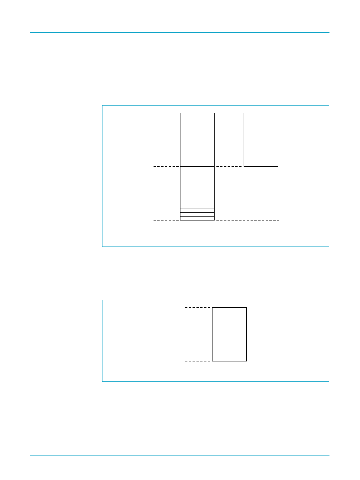
Philips Semiconductors
•
•
•
ISP1130
USB compound hub with keyboard controller
SFRs (80H to FFH): direct addressing
4 register banks (00H to 1FH): direct addressing; only 1 register bank may be
enabled at any time
Bit-addressable locations (20H to 2FH): direct addressing; these 16 bytes can
be used as 128 bit-addressable locations.
idth
Fig 5. Data memory organization.
10.2.2 Program memory
The ISP1130 has 8 kbytes of masked ROM for storing the 80C51 operating software.
In order to protect the ROM against illegal copying, execution of a MOVC instruction
from external code memory has been blocked. Instead of reading the program
memory, it accesses the on-chip data memory.
FFH
80H
7FH
20H
00H
INDIRECT
ADDRESSING
DIRECT &
INDIRECT
ADDRESSING
Data Memory Space
SFRs
DIRECT
ADDRESSING
ONLY
4 BANKS OF R0 to R7
MGS799
handbook, halfpage
1FFFH
8 kbytes
ON-CHIP
USER ROM
0000H
MGS800
Fig 6. Program memory organization.
10.3 Special function registers (SFRs)
The SFRs of the 80C51 can only be directly addressed. The memory map is given in
Table 47.
9397 750 06895
Objective specification Rev. 01 — 23 March 2000 35 of 68
© Philips Electronics N.V. 2000. All rights reserved.
Page 36

Philips Semiconductors
ISP1130
USB compound hub with keyboard controller
Table 47: SFR memory map
Address
range
(Hex)
F8 to FF WDTKEY WDT
F0 to F7 B
E8 to EF
E0 to E7 ACC
D8 to DF I2C0CON I2C0STA I2C0DAT I2C0ADR
D0 to D7 PSW
C8 to CF
C0 to C7 USBCON USBCONA
B8 to BF IP
B0 to B7 P3
A8 to AF IE
A0 to A7 P2
98 to 9F
90 to 97 P1
88 to 8F TCON TMOD TL0 TL1 TH0 TH1
80 to 87 P0 SP DPL DPH PCON
0 1 2 3 4 5 6 7
Offset
10.3.1 Program Status Word register (PSW)
The PSW register of the 80C51 is bit-addressable. The names and functions of the
bits are shown in Table 48 and Table 49.
Table 48: PSW register: bit allocation
7 6 5 4 3 2 1 0
CY AC F0 RS1 RS0 OV - P
Table 49: PSW register: bit description
[1]
Bit
PSW.7 CY carry flag; receives carry out from bit 7 of ALU operands
PSW.6 AC auxiliary carry flag; receives carry out from bit 3 of addition
PSW.5 F0 flag 0; general purpose status flag
PSW.4 RS1 register bank selector bit 1; see Table 50
PSW.3 RS0 register bank selector bit 0; see Table 50
PSW.2 OV overflow flag; set by arithmetic operations
PSW.1 - user-definable general purpose flag
PSW.0 P parity flag, indicating the number of ‘1’ bits in the accumulator
Symbol Description
operands
(logic 0 = even, logic 1 = odd); refreshed by hardware upon each
instruction cycle
[1] All bits are individually addressable.
9397 750 06895
Objective specification Rev. 01 — 23 March 2000 36 of 68
© Philips Electronics N.V. 2000. All rights reserved.
Page 37

Philips Semiconductors
ISP1130
USB compound hub with keyboard controller
Table 50: Register bank selection
RS1 RS0 Register bank Address range (Hex)
00 0 00to07
0 1 1 08 to 0F
10 2 10to17
11 3 18to1F
10.3.2 Power Control register (PCON)
Table 51: PCON register: bit allocation
Bit 7 6 5 4 3 2 1 0
Symbol - - - WLE GF1 GF0 PD IDL
Reset 000 0 0000
Access R/W R/W R/W R/W R/W R/W R/W R/W
Table 52: PCON register: bit description
Bit Symbol Description
7 to 5 - reserved
4 WLE Watchdog Load Enable. Writing a logic 1 enables writing to the
watchdog timer register and starts the watchdog timer for the first
time. A logic 0 disables writing to the watchdog timer register.
The watchdog timer can be stopped by writing 55H to the
WDTKEY register (see Table 70) or by a hardware reset.
3 GF1 General purpose flag set or reset by software.
2 GF0 General purpose flag set or reset by software.
1 PD Writing a logic 1 activates Power-down mode and switches off the
clock. When the microcontroller wakes up from Power-down mode
this bit is cleared to logic 0.
0 IDL Writinga logic 1 activatesIdle mode, switching off the normal clock
and turning on the sleep clock. A reset or interrupt returns the
microcontroller from Idle to normal mode and clears this bit to
logic 0.
10.3.3 USB Control register (USBCON)
Table 53: USBCON register: bit allocation
Bit 7 6 5 4 3 2 1 0
Symbol Self
Powered
Reset 011 1 1110
Access WWW W WWWW
9397 750 06895
Objective specification Rev. 01 — 23 March 2000 37 of 68
Enable
SYNCLK
Disable
KBDMatrix
GL-MEMSEL
Selection
Enable
OverCurrent
AnalogOC
Disable
Soft
Connect_N
© Philips Electronics N.V. 2000. All rights reserved.
Suspend
Clock
Page 38

Philips Semiconductors
Table 54: USBCON register: bit description
Bit Symbol Description
7 Self
6 Enable
5 Disable
4 GL-
3 Enable
2 AnalogOC
1 Soft
0 Suspend
Powered
SYNCLK
KBDMatrix
MEMSEL
Selection
Over
Current
Disable
Connect_N
Clock
ISP1130
USB compound hub with keyboard controller
A logic 0 selects bus-powered operation. A logic 1 enables(hybrid)
self-powered operation.
A logic 1 enables a 12 MHz clock signal on output SYNCLK, used
during external emulation of the microcontroller. A logic 0 disables
the clock signal on SYNCLK.
A logic 0 selects internal 82 kΩ pull-down resistors on the MYn
lines (keyboard matrix enabled). A logic 1 selects internal 8.2 kΩ
pull-up resistors on the MYn lines (keyboard matrix disabled).
A logic 0 enables upstream GoodLink indication, using output
MEMSEL/UPGL to drive the LED. A logic 1 configures pin
MEMSEL/UPGL as a chip select output for accessing an external
serial EEPROM via the I
A logic 1 configures pins
inputs. A logic 0 configures pins
GoodLink indicator outputs.
A logic 0 enables internal analog overcurrent sensing on pins
OCn/DPGLn (if enabled via bit EnableOverCurrent). A logic 1
selects digital overcurrent sensing.
A logic 0 connects an internal 1.5 kΩ pull-up resistor to the
upstream USB port (pin UP_DP). A logic 1 disables the pull-up
resistor.
A logic 1 switches off the clock after 2 ms following a ‘suspend’
interrupt. A logic 0 causes the clock to remain active during
‘suspend’ state. A change from logic 0 to logic 1 in the ‘suspend’
interrupt service routine switches off the clock after 1 ms.
2
C-bus interface.
OCn/DPGLn as overcurrent detection
OCn/DPGLn as downstream port
10.3.4 USB Control A register (USBCONA)
Table 55: USBCONA register: bit allocation
Bit 7 6 5 4 3 2 1 0
Symbol reserved PortCount1 PortCount0
Reset 00000001
Access WWWWWWWW
Table 56: USBCONA register: bit description
Bit Symbol Description
7 to 2 - reserved
1, 0 PortCount[1:0] number of enabled embedded functions:
00 — undefined
01 — 1 embedded function (default)
10 — 2 embedded functions
11 — 3 embedded functions
9397 750 06895
Objective specification Rev. 01 — 23 March 2000 38 of 68
© Philips Electronics N.V. 2000. All rights reserved.
Page 39

Philips Semiconductors
10.4 Hub control registers
The hub control registers (Command and Data) are mapped to the external data
memory space of the 80C51 as shown in Table 57. To access these registers use a
MOVX instruction.
Table 57: Hub control registers: address mapping
Register Access Address (Hex)
Command write FFFE
Data read/write FFFF
10.5 Interrupt structure
The ISP1130 implements a 6-source interrupt structure with 2 priority levels. The
interrupt vector addresses and polling sequence is given in Table 58. The interrupt
priority levels are set via the Interrupt Polarity (IP) register (see Table 61) and the
interrupts can be enabled or disabled via the Interrupt Enable (IE) register (see
Table 59).
Table 58: Interrupt vectors and polling sequence
Source Description Vector address
EX0 external 0 interrupt (USB) 0003H
ET0 timer 0 interrupt 000BH
EX1 external 1 interrupt (keyboard) 0013H
ET1 timer 1 interrupt 001BH
I2C I
IN2 external 2 interrupt (input
USB compound hub with keyboard controller
2
C-bus interrupt 0023H
INT) 002BH
ISP1130
External interrupt 0 (EX0) is generated by the USB core when an activity occurs for
any of the three embedded functions. Interrupt EX0 is level-triggered and sets bit IE0
in the TCON register. IE0 is cleared by hardware when the service routine is entered.
External interrupt 1 (EX1) is generated by a key press in the matrix. Interrupt EX1 is
level-triggered and sets bit IE1 in the TCON register. IE1 is cleared by hardware
when the service routine is entered. When the device is in ‘suspend’ state (the
microcontroller clock is disabled), interrupt EX1 is registered and an internal Remote
Wakeupis generated to restart the PLL and the clocks. When the device resumes its
function and the clock to microcontroller core has been restored, the firmware
branches to the interrupt service routine for EX1.
External interrupt 2 (IN2) is generated by input pin INT, which is edge-triggered
(HIGH-to-LOW transition).
Timer 0 and Timer 1 interrupts are generated by a timer register overflow (except for
Timer 0 in Mode 3), signalled by bits TF0 and TF1 in the TCON register. The bit that
generated the interrupt is cleared by hardware, when the service routine is entered.
9397 750 06895
Objective specification Rev. 01 — 23 March 2000 39 of 68
© Philips Electronics N.V. 2000. All rights reserved.
Page 40

Philips Semiconductors
ISP1130
USB compound hub with keyboard controller
Table 59: IE register: bit allocation
Bit 7 6 5 4 3 2 1 0
Symbol EA - IN2 I2C ET1 EX1 ET0 EX0
Reset 000 0 0000
Access R/W R/W R/W R/W R/W R/W R/W R/W
Table 60: IE register: bit description
[1]
Bit
IE.7 EA enable all interrupts; a logic 0 disables all interrupts, a logic 1
IE.6 - reserved
IE.5 IN2 A logic 1 enables external interrupt 2 (input
IE.4 I2C A logic 1 enables I
IE.3 ET1 A logic 1 enables Timer 1 overflow interrupt
IE.2 EX1 A logic 1 enables external interrupt 1 (keyboard)
IE.1 ET0 A logic 1 enables Timer 0 overflow interrupt
IE.0 EX0 A logic 1 enables external interrupt 0 (USB)
Symbol Description
allows all interrupt sources to be individually enabled or disabled
2
C interrupt
INT)
[1] All bits are individually addressable.
Table 61: IP register: bit allocation
Bit 7 6 5 4 3 2 1 0
Symbol - - IN2 I2C ET1 EX1 ET0 EX0
Reset XX0 0 0000
Access R/W R/W R/W R/W R/W R/W R/W R/W
Table 62: IP register: bit description
Bit
[1]
Symbol Description
[2]
IP.7 - reserved
IP.6 - reserved
IP.5 IN2 priority of external interrupt 2 (input
2
IP.5 I2C priority of I
C interrupt
INT)
IP.3 ET1 priority of Timer 1 interrupt
IP.2 EX1 priority of external interrupt 1 (keyboard)
IP.1 ET0 priority of Timer 0 interrupt
IP.0 EX0 priority of external 0 (USB) interrupt
[1] All bits are individually addressable.
[2] A logic 0 indicates a LOW priority, a logic 1 indicates a HIGH priority.
10.6 Timers/counters
The ISP1130 contains two 16-bit timer/counters (Timer 0 and Timer 1), which are
used for generating interrupt requests. Each timer has a control bit C/T in the Timer
Control register (TCON, see Table 67), which selects the timer or counter function. In
the ISP1130 this bit must always be 0 for timer operation.
9397 750 06895
Objective specification Rev. 01 — 23 March 2000 40 of 68
© Philips Electronics N.V. 2000. All rights reserved.
Page 41

Philips Semiconductors
Both timers can be programmed independently to operate in 4 different modes via the
Timer Mode register (TMOD, see Table 63). When Timer 0 is in mode 3, Timer 1 can
be programmed to modes 0, 1 or 2 but it cannot set an interrupt request flag or
generate an interrupt.
Table 63: TMOD register: bit allocation
Timer 1: bits 7 to 4; Timer 0: bits 3 to 0
Table 64: TMOD register: bit description
Bit Symbol Description
7 GATE Timer 1 counter gate control; must always be 0
6C/
5 M1 Timer 1 mode selector bit 1; see Table 63
4 M0 Timer 1 mode selector bit 0; see Table 63
3 GATE Timer 0 counter gate control; must always be 0
2C/
1 M1 Timer 0 mode selector bit 1; see Table 63
0 M0 Timer 0 mode selector bit 0; see Table 63
ISP1130
USB compound hub with keyboard controller
7 6 5 4 3 2 1 0
GATE C/
TM1M0GATEC/TM1M0
T Timer 1 counter/timer select; must always be 0
T Timer 0 counter/timer select; must always be 0
Table 65: Timer mode selection
M1, M0 Mode Description
00 0 13-bit timer
01 1 16-bit timer
10 2 8-bit auto-reload timer
11 3 Timer 0:TL0 is an 8-bit timer controlled by Timer 0 control bits;
TH0 is an 8-bit timer controlled by Timer 1 control bits
Timer 1: stopped
Each timer consists of two 8-bit registers in the SFR memory space: TLn and THn
(see Table 66). The timer registers are incremented every machine cycle of the
80C51 core. Since one machine cycle consists of 6 clock periods, the timer counts at
a rate of1⁄6× f
MCU_CLOCK
. This corresponds with 2 MHz for the default microcontroller
clock frequency of 12 MHz.
Table 66: Timer register addresses
Register SFR address Description
TL0 8AH Timer0: lower byte
TH0 8CH Timer 0: upper byte
TL1 8BH Timer1: lower byte
TH1 8DH Timer 1: upper byte
The timers are started and stopped under software control via the SFR TCON (see
Table 67). Each timer sets its interrupt request flag when the timer register overflows
from all 1’sto all 0’s (normal timer) or to the reload value (auto-reload timer). When a
timer interrupt is generated, the corresponding interrupt request flag is cleared by the
hardware upon entering the interrupt service routine.
9397 750 06895
Objective specification Rev. 01 — 23 March 2000 41 of 68
© Philips Electronics N.V. 2000. All rights reserved.
Page 42

Philips Semiconductors
ISP1130
USB compound hub with keyboard controller
Table 67: TCON register: bit allocation
Bit 7 6 5 4 3 2 1 0
Symbol TF1 TR1 TF0 TR0 IE1 IT1 IE0 IT0
Reset 000 0 0 000
Access R R/W R R/W R R/W R R/W
Table 68: TCON register: bit description
[1]
Bit
TCON.7 TF1 Timer 1 overflow flag; set by hardware upon Timer 1 overflow;
TCON.6 TR1 Timer 1 run control bit; 0 = timer OFF, 1 = timer ON
TCON.5 TF0 Timer 0 overflow flag; set by hardware upon Timer 0 overflow;
TCON.4 TR0 Timer 0 run control bit; 0 = timer OFF, 1 = timer ON
TCON.3 IE1 external interrupt 1 flag; set by hardware when a keyboard
TCON.2 IT1 triggering mode for external interrupt 1, set by software;
TCON.1 IE0 external interrupt 0 flag; set by hardware when a USB core
TCON.0 IT0 triggering mode for external interrupt 0, set by software;
Symbol Description
cleared by hardware upon entering the interrupt service routine
cleared by hardware upon entering the interrupt service routine
interrupt is detected; cleared by hardware upon entering the
interrupt service routine
must always be logic 0 (= HIGH-to-LOW transition)
interrupt is detected; cleared by hardware upon entering the
interrupt service routine
must always be 0 (= HIGH-to-LOW transition)
[1] All bits are individually addressable.
10.7 Watchdog timer
The Watchdog timer is a counter that resets the microcontroller upon overflow. This
allows recovery from erroneous processor states (e.g. caused by electrical noise or
RF-interference). To prevent the Watchdog timer from overflowing, the software must
reload the counter within a predefined (programmable) time.
The Watchdog timer is a 19-bit counter,consisting of an 11-bit prescaler and an 8-bit
SFR (WDT). The counter is clocked in state 2 of every CPU cycle (= 6 clocks) and
generates a reset when register WDT overflows. For a 12 MHz clock frequency, the
interval between overflowscan be programmed between 1.024 ms (WDT = FFH) and
262.144 ms (WDT = 00H). After a reset the WDT register contains all zeroes.
Toenable loading of the Watchdogtimer, bit WLE in the PCON register must be set to
logic 1 (see Table 51). When this is done for the first time, it also starts the timer. The
Watchdog timer can be disabled by writing 55H to the WDTKEY register, or by a
hardware reset.
Table 69: Watchdog timer registers: address mapping
Register Access Address (Hex)
WDTKEY write FE
WDT write FF
9397 750 06895
Objective specification Rev. 01 — 23 March 2000 42 of 68
© Philips Electronics N.V. 2000. All rights reserved.
Page 43

Philips Semiconductors
ISP1130
USB compound hub with keyboard controller
Table 70: WDTKEY register: bit allocation
Bit 7 6 5 4 3 2 1 0
Symbol WDK[7:0]
Reset 01010101
Access WWWWWWWW
Table 71: WDTKEY register: bit description
Bit Symbol Description
7 to 0 WDK[7:0] Watchdog Key: a value of 55H disables the Watchdog timer and
inhibits the setting of bit PD in the PCON register. Any other value
than 55H will (re)enable the Watchdog timer.
Table 72: WDT register: bit allocation
Bit 7 6 5 4 3 2 1 0
Symbol WDL[7:0]
Reset 00000000
Access WWWWWWWW
Table 73: WDT register: bit description
Bit Symbol Description
7 to 0 WDL[7:0] Watchdog Load value. The Watchdog timer interval is given by
(256 − WDL) in units of 1.024 ms (12 MHz clock frequency).
[1] This register can only be written if bit WLE in the PCON register is set to logic 1.
10.7.1 Watchdog timer software example
The following example shows how the Watchdog timer operation might be handled in
a user program.
;at program start
WDT EQU 0FFH ;address of watchdog timer SFR
PCON EQU 087H ;address of power-control SFR
WDT_INT EQU 156 ;WDT internal 100 * prescaler overflow
;call to subroutine which reloads the WDT
LCALL WATCHDOG
;watchdog subroutine
WATCHDOG: ORL PCON,#10H ;set WLE bit in PCON
MOV WDT,#WDT_INT ;load watchdog timer with interval
RET
9397 750 06895
Objective specification Rev. 01 — 23 March 2000 43 of 68
© Philips Electronics N.V. 2000. All rights reserved.
Page 44

Philips Semiconductors
10.8 I/O description
The following groups of I/O lines are available for interfacing a keyboard matrix to the
ISP1130:
MX0 to MX7 — return lines for keyboard matrix; inputs with internal 8.2 kΩ pull-up
resistors, 5 V tolerant. Inputs MX3 and MX4 are multiplexed with the SCL and SDA
lines respectively. This allows the ISP1130 firmware to read configuration data from
an external EEPROM via SDA and SCL, e.g. upon a hardware or a USB bus reset.
MY0 to MY17 — scan lines for keyboardmatrix; bidirectional lines with internal 82 kΩ
pull-down resistors and 8.2 kΩ pull-up resistors. The pull-down resistors are selected
by setting bit DisableKBDMatrix in the USBCON register.In Idle mode these lines are
inputs, which are OR-ed together to generate an interrupt when a key is pressed.
CAPSLOCK / NUMLOCK / SCRLOCK — open drain outputs for driving Caps Lock,
Num Lock and Scroll Lock indicator LEDs (max. 8 mA).
Remark: When accessing external functions or devices via the ISP1130 bus lines, it
is recommended to isolate the MYn lines by means of analog switches,controlled via
output MEMSEL/UPGL. This prevents bus conflicts during keyboard scanning.
ISP1130
USB compound hub with keyboard controller
10.9 I/O port mapping
Table 74 provides the mapping of standard 80C51 input/output ports with respect to
their use in ISP1130.
Table 74: Mapping of I/O ports between ISP1130 and 80C51
ISP1130 ports 80C51 ports Description
MY0 to MY7 P0.0 to P0.7 keyboard scan lines
MY8 to MY15 P2.0to P2.7 keyboard scan lines
MY16 P1.0 keyboard scan lines
MY17 P1.1 keyboard scan lines
MEMSEL/UPGL P1.2 chip select output for an external EEPROM;
upstream port GoodLink indicator output
CAPSLOCK P1.3 control output for Caps Lock LED indicator
NUMLOCK P1.4 control output for Num Lock LED indicator
SCRLOCK P1.5 control output for Scroll Lock LED indicator
n.c. P1.6 not used
n.c. P1.7 not used
MX0 to MX7 P3.0 to P3.7 keyboard return lines
10.10 Keyboard matrix implementation
The ISP1130 can support a maximum key matrix size of 18 × 8, totalling 144 keys. A
typical implementation of the keyboard matrix is shown in Figure 7.
9397 750 06895
Objective specification Rev. 01 — 23 March 2000 44 of 68
© Philips Electronics N.V. 2000. All rights reserved.
Page 45
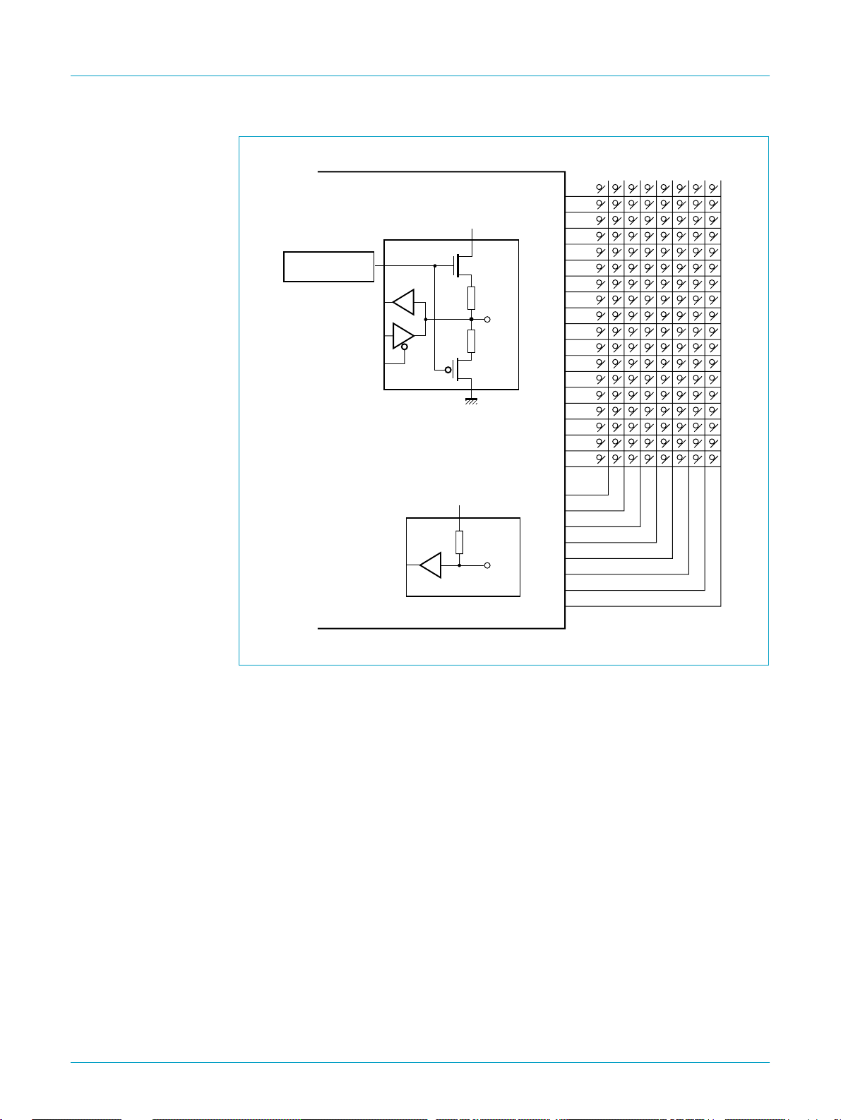
Philips Semiconductors
ISP1130
USB compound hub with keyboard controller
idth
DisableKBDMatrix
(USBCON register)
internal circuit
ISP1130
internal circuit
V
V
CC
CC
8.2 kΩ
82 kΩ
8.2 kΩ
MYn
MXn
MY0
MY1
MY2
MY3
MY4
MY5
MY6
MY7
MY8
MY9
MY10
MY11
MY12
MY13
MY14
MY15
MY16
MY17
MX0
MX1
MX2
MX3
MX4
MX5
MX6
MX7
Keyboard matrix
MGS801
Fig 7. Typical keyboard matrix implementation.
The keyboard scanning algorithm is as follows:
1. When no key press is detected within a predefined time interval, the
microcontroller switches the MYn scan lines to ‘input’ and enters Idle mode.
2. Pressing any key will result in the HIGH level of an MXn line to be transferred to
an MYn input. Such a HIGH level (4.45 V typ.) exceeds VIH and generates an
interrupt, since all MYn lines are OR-ed together.
3. Upon a keyboard interrupt the microcontroller exits Idle mode and resumes
standard keyboard matrix scanning to determine which key was pressed.
This algorithm helps to reduce EMI and power consumption.
10.11 Suspend and resume
10.11.1 Suspend
When there is no activity on the USB bus for more than 3 ms, the device generates
an interrupt to the microcontroller to enter ‘suspend’ state.
The microcontroller can respond to a ‘suspend’ interrupt in three ways,depending on
the value of bit SuspendClock in the USBCON register when servicing the interrupt:
9397 750 06895
Objective specification Rev. 01 — 23 March 2000 45 of 68
© Philips Electronics N.V. 2000. All rights reserved.
Page 46

Philips Semiconductors
•
•
•
Remark: After a resume operation, the microcontroller has to clear bit SuspendClock
to logic 0 to enable further suspend operations.
10.11.2 Resume
The ISP1130 can resume operation from ‘suspend’ state in three ways, depending on
whether the operating clocks are active or not:
•
•
ISP1130
USB compound hub with keyboard controller
SuspendClock = 0: The operating clocks of the USB core and the microcontroller
remain on during ‘suspend’ state. The device’s power consumption is not reduced
and therefore this state does not guarantee ‘suspend’ current requirements.
SuspendClock = 1: The internal clocks are automatically switched off after 2 ms.
This allows the microcontroller adequate time to process the ‘suspend’ interrupt
and enter Power-down mode. Power consumption is reduced to its minimum to
meet the ‘suspend’ current requirements of
SuspendClock is changed from 0 to 1: The clocks are switched off after 1 ms.
This option can be used if the microcontroller requires more time than 2 ms to
prepare for ‘suspend’ mode.
Operating clock on: Clearing the Suspend bit of the Device Status Register to
logic 0 will generate a remote wake-up signal.
Operating clock off: The following events will generate a remote wake-up signal:
– Key press (activity on the MYn lines)
– USB bus activity.
Upon a remote wake-upsignal, the USB core first enables the PLL and the clocks.
When the clocks have stabilized, an interrupt wakes up the microcontroller from
Power-down mode. The microcontroller resumes program execution from where it
left off. A ‘resume’ signal is then generated on the upstream port.
USB Specification Rev. 1.1
.
11. I2C-bus interface
A simple I2C-bus interface is provided in the ISP1130 to read configuration data from
an external EEPROM upon a (power-on) reset or a bus reset from the USB host. The
interface hardwaresupports both single master and slaveoperation at bus speeds up
to 400 kHz.
For this application the user must configure the I2C-bus interface as single master via
software. After reading the EEPROM configuration data, the I2C-bus driver software
module and the EEPROM must be disabled, since the SCL and SDA lines are
multiplexed with keyboard matrix scan lines (MX3 and MX4 respectively). Output
MEMSEL/UPGL is available for (de)selecting the EEPROM.
The I2C-bus interfaceis intended for bidirectional communication between ICs via two
serial bus wires, SDA (data) and SCL (clock). Both lines are driven by open-drain
circuits and must be connected to the positive supply voltage via pull-up resistors. In
the ISP1130 8.2 kΩ pull-up resistors are integrated on pins MX3/SCL and MX4/SDA.
9397 750 06895
Objective specification Rev. 01 — 23 March 2000 46 of 68
© Philips Electronics N.V. 2000. All rights reserved.
Page 47
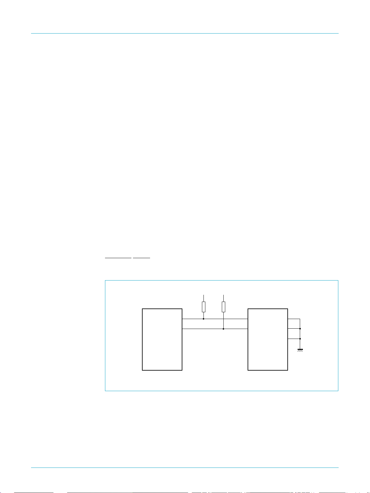
Philips Semiconductors
11.1 Protocol
The I2C-bus protocol defines the following conditions:
•
•
•
•
Each device on the I2C-bus has a unique slave address, which the master uses to
select a device for access.
The master starts a data transfer using a START condition and ends it by generating
a STOP condition. Transfers can only be initiated when the bus is free. The receiver
must acknowledge each byte by means of a LOW levelon SDAduring the ninth clock
pulse on SCL.
ISP1130
USB compound hub with keyboard controller
Bus free: both SDA and SCL are HIGH
START: a HIGH-to-LOW transition on SDA, while SCL is HIGH
STOP: a LOW-to-HIGH transition on SDA, while SCL is HIGH
Data valid: after a START condition, data on SDA are stable during the HIGH
period of SCL; data on SDA may only change while SCL is LOW.
For detailed information please consult
9398 393 40011.
11.2 Hardware connections
Via the I2C-bus interface the ISP1130 can be connected to an external EEPROM
(PCF8582 or equivalent). The hardware connections are shown in Figure 8.
The SCL and SDA pins are multiplexed with pins MX3 and MX4 respectively. Pin
MEMSEL/UPGL can be used as a chip select output to select external devices, such
as smart card readers, UARTs, etc.
dth
MX3/SCL
MX4/SDA
ISP1130
USB HUB
The I2C-bus and how to use it
DD
R
2
I
C-bus
V
DD
R
P
P
SCL
SDA
PCF8582
EEPROM
equivalent
V
., order number
A0
A1
A2
or
MGS808
Fig 8. EEPROM connection diagram.
The slave address which ISP1130 uses to access the EEPROM is 1010000B. Page
mode addressing is not supported, so pins A0, A1 and A2 of the EEPROM must be
connected to GND (logic 0).
9397 750 06895
Objective specification Rev. 01 — 23 March 2000 47 of 68
© Philips Electronics N.V. 2000. All rights reserved.
Page 48

Philips Semiconductors
ISP1130
USB compound hub with keyboard controller
11.3 Data transfer
The I2C-bus interface can be used to read configuration data from an external
EEPROM, e.g. upon a hardware or USB bus reset. The EEPROM must be enabled
and disabled using output pin MEMSEL/UPGL. To select the I2C-bus function of pins
MX3/SCL and MX4/SDA, bit ENS1 in the I2C0CON register must be set to logic 1.
The number and the organization of the data bytes read from the EEPROM can be
determined by the firmware designer.
The I2C-bus interface is accessed via a number of SFRs, shown in Table 75.
Table 75: I2C register addresses
Register SFR address Description
2
I2C0CON D8H I
I2C0STA D9H I
I2C0DAT DAH I
I2C0ADR DBH I
Table 76: I2C0CON register: bit allocation
Bit 7 6 5 4 3 2 1 0
Symbol CR2 ENS1 STA STO SI AA CR1 CR0
Reset 000 0 0 000
Access R/W R/W R/W R/W R/W R/W R/W R/W
C-bus control register
2
C-bus status register
2
C-bus data register
2
C-bus address register
Table 77: I2C0CON register: bit description
[1]
Bit
I2C0CON.7 CR2 selects I
I2C0CON.6 ENS1 Enable Serial I/O. A logic 1 enables the I
Symbol Description
2
C-bus bit frequency in Master mode, see Table 78
2
C-bus interface
and sets pins MX3/SCL and MX4/SDA to logic 1. A logic 0
2
disables the I
C-bus interface and clears bit STO to logic 0,
allowing MX3/SCL and MX4/SDA to be used as open drain
I/O pins.
I2C0CON.5 STA START flag. In Slave mode a logic1 generates a START
condition as soon as the bus is free. In Master mode a
logic 1 generates a repeated START condition.
I2C0CON.4 STO STOP flag. In maSter mode a logic 1 generates a STOP
condition. This bit is cleared by hardware if a STOP
condition is detected on the bus. In Slavemode a logic 1can
be used to recover from an error: it causes SDAand SCL to
be released and the device to be unaddressed.
I2C0CON.3 SI Serial Interrupt flag. A logic 1 signals a validstatus change
(see Table 83), causing the SCL LOW period to be stretched
and the transfer to be suspended. This bit must be cleared
by software when servicing the interrupt.
9397 750 06895
Objective specification Rev. 01 — 23 March 2000 48 of 68
© Philips Electronics N.V. 2000. All rights reserved.
Page 49

Philips Semiconductors
ISP1130
USB compound hub with keyboard controller
Table 77: I2C0CON register: bit description
[1]
Bit
I2C0CON.2 AA Assert Acknowledge. A logic 1 indicates that an ACK (low
I2C0CON.1 CR1 selects I
I2C0CON.0 CR0 selects I
[1] All bits are individually addressable.
Table 78: I
CR2 CR1 CR0 I2C-bus bit frequency (12 MHz oscillator)
0 0 0 200 kHz
0 0 1 7.5 kHz
0 1 0 300 kHz
0 1 1 400 kHz
1 0 0 50 kHz
1 0 1 3.75 kHz
1 1 0 75 kHz
1 1 1 100 kHz
Symbol Description
levelon SDA during acknowledge pulse on SCL) is returned
for one of the following conditions:
own slave address received
•
General Call address received, if bit GC = 1 (I2C0CON)
•
data byte received when in master receive mode
•
data byte received when addressed in slave receiver
•
mode.
2
C-bus bit frequency (Master mode)
…continued
2
C-bus bit frequency in Master mode, see Table 78
2
C-bus bit frequency in Master mode, see Table 78
Table 79: I2C0DAT register: bit allocation
Bit 7 6 5 4 3 2 1 0
Symbol SD[7:0]
Reset 00000000
Access R/W R/W R/W R/W R/W R/W R/W R/W
Table 80: I2C0DAT register: bit description
Bit Symbol Description
[1]
7 to 0 SD[7:0]
[1] Bits are transmitted or received MSB (SD7) first.
Table 81: I2C0STA register: bit allocation
Bit 7 6 5 4 3 2 1 0
Symbol SC[4:0] - - -
Reset 11111000
Access RRRRRRRR
9397 750 06895
Objective specification Rev. 01 — 23 March 2000 49 of 68
DATA byte (just received or to be transmitted); a logic 0 value
corresponds with a LOW level on SDA, a logic 1 with a HIGH
level
© Philips Electronics N.V. 2000. All rights reserved.
Page 50

Philips Semiconductors
Table 82: I2C0STA register: bit description
Bit Symbol Description
7 to 3 SC[4:0] status code, see Table 83
2 to 0 - reserved, always zero
Table 83: I
Status byte SC[4:0] Description (see Table 84)
Master transmit mode
08H 00001 START condition has been transmitted
10H 00010 repeated START condition has been transmitted
18H 00011 SLA and W have been transmitted, ACK was received
20H 00100 SLA and W have been transmitted,
28H 00101 DATA byte has been transmitted, ACK was received
30H 00110 DATA byte has been transmitted,
38H 00111 arbitration was lost in SLA, R/W or DATA byte
Master receive mode
08H 00001 START condition has been transmitted
10H 00010 repeated START condition has been transmitted
38H 00111 arbitration was lost while returning
40H 01000 SLA and R have been transmitted, ACK was received
48H 01001 SLA and R have been transmitted,
50H 01010 DATA byte has been received, ACK was returned
58H 01011 DATA byte has been received,
Slave receive mode
60H 01100 own SLA and W have been received, ACK was returned
68H 01101 arbitration was lost in SLA, R/W as master; own SLA and W
70H 01110 General Call has been received, ACK was returned
78H 01111 arbitration was lost in SLA, R/W as master; General Call has
80H 10000 previously addressed with own SLA; DATA byte has been
88H 10001 previously addressed with own SLA; DATA byte has been
90H 10010 previously addressed with General Call; DATA byte has been
98H 10011 previously addressed with General Call; DATA byte has been
A0H 10100 STOP or repeated START condition has been received, while
2
C-bus status codes
USB compound hub with keyboard controller
ACK was received
ACK was received
ACK
ACK was received
ACK was returned
have been received, ACK was returned
been received
received, ACK was returned
received,
received, ACK was returned
received,
still addressed as slave receiver or transmitter
ACK was returned
ACK was returned
ISP1130
9397 750 06895
Objective specification Rev. 01 — 23 March 2000 50 of 68
© Philips Electronics N.V. 2000. All rights reserved.
Page 51

Philips Semiconductors
ISP1130
USB compound hub with keyboard controller
Table 83: I
2
C-bus status codes
…continued
Status byte SC[4:0] Description (see Table 84)
Slave transmit mode
A8 10101 own SLA and R have been received, ACK was returned
B0 10110 arbitration was lost in SLA, R/W as master; own SLA and R
have been received, ACK was returned
B8 10111 DATA byte has been transmitted, ACK was received
C0 11000 DATA byte has been transmitted,
ACK was received
C8 11001 last DATA byte has been transmitted (AA = 0 in I2C0CON),
ACK was received
Miscellaneous
00H 00000 bus error in master or addressed slave mode, caused by
erroneous START or STOP condition
F8H 11111 no relevant status information is available; bit SI in the
I2C0CON register is cleared to logic 0
2
Table 84: Symbols used in I
C-bus
Symbol Description
SLA slave address (7 bits)
R read bit (logic 1)
W write bit (logic 0)
ACK acknowledgment (logic 0)
ACK no acknowledgment (logic 1)
2
DATA data byte to or from I
C-bus
Table 85: I2C0ADR register: bit allocation
Bit 7 6 5 4 3 2 1 0
Symbol SA[6:0] GC
Reset 00000000
Access R/W R/W R/W R/W R/W R/W R/W R/W
Table 86: I2C0ADR register: bit description
Bit Symbol Description
7 to 1 SA[6:0] own slave address of the microcontroller; only used in Slave
mode, ignored in Master mode
0 GC A logic 1 causes the device to respond to a General Call
address (00H). A logic 0 lets the device ignore address 00H.
9397 750 06895
Objective specification Rev. 01 — 23 March 2000 51 of 68
© Philips Electronics N.V. 2000. All rights reserved.
Page 52
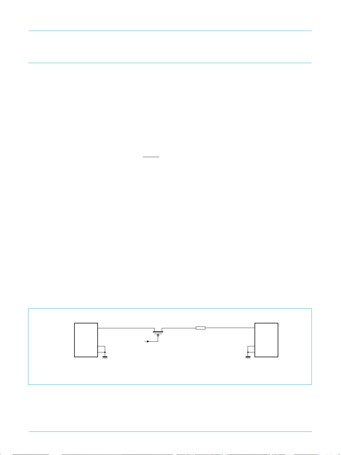
Philips Semiconductors
12. Hub power modes
USB hubs can either be self-powered or bus-powered.
Self-powered — Self-powered hubs have a 5 V local power supply on board which
provide power to the hub and the downstream ports. The
requires that these hubs limit the current to 500 mA per downstream port and report
overcurrent conditions to the host. The hub may optionally draw 100 mA from the
USB supply (V
Bus-powered — Bus-powered hubs obtain all power from the host or an upstream
self-powered hub. The maximum current is 100 mA per downstream port. Current
limiting and reporting of overcurrent conditions are both optional.
The ISP1130 has bus-powered downstream ports and supports individual power
switching via pins PSWn.
12.1 Voltage drop requirements
12.1.1 Bus-powered hubs
Bus-powered hubs are guaranteed to receive a supply voltage of 4.5 V at the
upstream port connector and must provide a minimum of 4.4 V to the downstream
port connectors. The voltage drop of 100 mV across bus-powered hubs includes:
USB compound hub with keyboard controller
USB Specification Rev. 1.1
) to power the interface functions (hybrid-powered).
BUS
ISP1130
Hub PCB (power and ground traces, ferrite beads)
•
Power switch (FET on-resistance)
•
Overcurrent sense device.
•
The PCB resistance may cause a drop of 25 mV, which leaves 75 mV for the power
switch and overcurrent sense device. The voltage drop components are shown in
Figure 9.
For bus-powered hubs overcurrent protection is optional. It may be implemented for
all downstream ports on a global or individual basis. The ISP1130 has individual
overcurrent protection for its downstream ports.
handbook, full pagewidth
V
BUS
upstream
port
connector
(1) Includes PCB traces, ferrite beads, etc.
D+
D−
GND
SHIELD
voltage drop
ISP1122
power
switch
75 mV
low-ohmic
PMOS switch
Fig 9. Typical voltage drop components in bus-powered mode (no overcurrent detection).
voltage drop
25 mV
hub board
resistance
4.40 V(min)4.50 V(min)
(1)
V
BUS
D+
D−
GND
SHIELD
MGR783
downstream
port
connector
9397 750 06895
Objective specification Rev. 01 — 23 March 2000 52 of 68
© Philips Electronics N.V. 2000. All rights reserved.
Page 53

Philips Semiconductors
13. Overcurrent detection
The ISP1130 has an analog overcurrent detection circuit for monitoring downstream
port lines. This circuit automatically reports an overcurrent condition to the host and
turns off the power to the faulty port. The host must reset the condition flag.
Pins OC1/DPGL1 and OC2/DPGL2 can be used for individual port overcurrent
detection or GoodLink indication. The pin functionality is selected via bit
EnableOverCurrent in the USBCON register, see Table 53.
13.1 Overcurrent circuit description
The integrated overcurrent detection circuit of ISP1130 senses the voltage drop
across the power switch or an extra low-ohmic sense resistor. When the port draws
too much current, the voltage drop across the power switch exceeds the trip voltage
threshold (∆V
switch control signal after a delay of 15 ms (t
period to minimize false tripping, especially during the inrush current produced by ‘hot
plugging’ of a USB device.
ISP1130
USB compound hub with keyboard controller
). The overcurrent circuit detects this and switches off the power
trip
). This delay acts as a ‘debounce’
trip
13.2 Power switch selection
Fromthe voltagedrop analysis given in Figure 9, the power switchhas a voltage drop
budget of 75 mV. For individual self-powered mode,the current drawnper port can be
up to 500 mA. Thus the power switch should have maximum on-resistance of
150 mΩ.
If the voltage drop due to the hub board resistance can be minimized, the power
switch can have more voltage drop budget and therefore a higher on-resistance.
Power switches with a typical on-resistance of around 100 mΩ fit into this application.
The ISP1130 overcurrent detection circuit has been designed with a nominal trip
voltage (∆V
) of 85 mV. This gives a typical trip current of approximately 850 mA for
trip
a power switch with an on-resistance of 100 mΩ1.
13.3 Tuning the overcurrent trip voltage
The ISP1130 trip voltage can optionally be adjusted through external components to
set the desired trip current. This is done by inserting tuning series resistors at pins
OCn/DPGLn (see Figure 10). Rtd tunes down the trip voltage ∆V
Equation 1.
∆V
with I
trip
OC(nom)
∆V
trip intrinsic()
= 0.5 µA.
I
⋅–=
OCRtd
according to
trip
(1)
1. The following PMOS power switches have been tested to work well with the ISP1130: Philips PHP109, Vishay Siliconix Si2301DS,
Fairchild FDN338P.
9397 750 06895
Objective specification Rev. 01 — 23 March 2000 53 of 68
© Philips Electronics N.V. 2000. All rights reserved.
Page 54
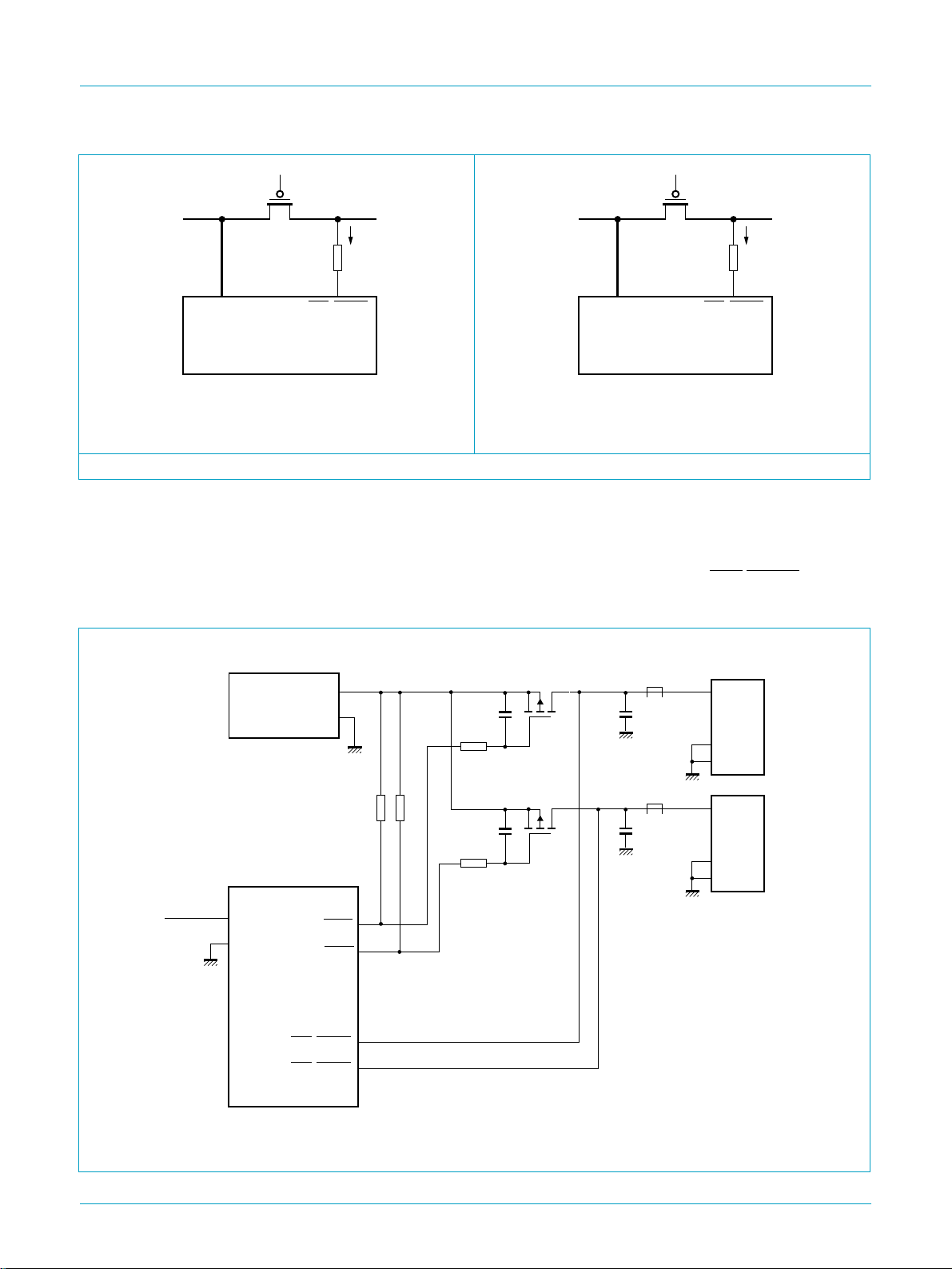
Philips Semiconductors
ISP1130
USB compound hub with keyboard controller
handbook, halfpage
V
CC
low-ohmic
PMOS switch
I
OC
R
td
V
CC
OCn/DPGLn
handbook, halfpage
V
BUS
V
CC
ISP1130
MBL161
I
= 0.5 µAI
OC(nom)
OC(nom)
= 0.5 µA
a. Hybrid-powered mode. b. Bus-powered mode.
Fig 10. Tuning the overcurrent trip voltage.
13.4 Reference circuit
A typical example of individual port power switching and individual overcurrent
detection is given in Figure 11. The RC circuit (10 kΩ and 1 µF) around the PMOS
switch provides for soft turn-on. Series resistors between pins OCn/DPGLn and the
supply voltage maybe used to tunedownthe overcurrent trip voltage (see Figure 10).
ISP1130
low-ohmic
PMOS switch
R
OCn/DPGLn
MBL160
I
OC
td
handbook, full pagewidth
+4.85 V(min)
5 V
POWER SUPPLY
± 3%
V
CC
GND
ISP1130
OC1/DPGL1
OC2/DPGL2
+4.85 V(min)
+
−
330 kΩ
(2×)
PSW1
PSW2
0.1 µF
10 kΩ
0.1 µF
10 kΩ
low-ohmic
PMOS switch
low-ohmic
PMOS switch
downstream
(min)
(min)
ports
V
BUS
D+
D−
GND
SHIELD
V
BUS
D+
D−
GND
SHIELD
1
2
ferrite bead
1
2
120
µF
ferrite bead
120
µF
MBL162
+4.75 V
+4.75 V
Power switches 1 and 2 are low-ohmic PMOS devices as specified in Section 13.2.
Fig 11. Hybrid-powered hub; individual port power switching; individual overcurrent detection.
9397 750 06895
Objective specification Rev. 01 — 23 March 2000 54 of 68
© Philips Electronics N.V. 2000. All rights reserved.
Page 55

Philips Semiconductors
ISP1130
USB compound hub with keyboard controller
14. Limiting values
Table 87: Absolute maximum ratings
In accordance with the Absolute Maximum Rating System (IEC 60134).
Symbol Parameter Conditions Min Max Unit
V
CC
V
I
I
latchup
V
esd
T
stg
P
tot
[1] Equivalent to discharging a 100 pF capacitor via a 1.5 kΩ resistor (Human Body Model).
[2] Values are given for device only; in-circuit V
[3] For open-drain pins V
Table 88: Recommended operating conditions
Symbol Parameter Conditions Min Max Unit
V
CC
V
I
V
I(AI/O)
V
O(od)
T
amb
supply voltage −0.5 +6.0 V
input voltage −0.5 - V
latchup current VI< 0 or VI>V
electrostatic discharge voltage ILI<15µA
CC
- 200 mA
[1] [2]
- ±4000
[3]
V
storage temperature −60 +150 °C
total power dissipation - <tbf> mW
= ±8000 V.
esd(max)
= ±2000 V.
esd(max)
supply voltage 4.0 5.5 V
input voltage 0 5.5 V
input voltage on analog I/O pins
0 3.6 V
(D+/D−)
open-drain output pull-up voltage 0 5.5 V
operating ambient temperature −40 +85 °C
9397 750 06895
Objective specification Rev. 01 — 23 March 2000 55 of 68
© Philips Electronics N.V. 2000. All rights reserved.
Page 56

Philips Semiconductors
ISP1130
USB compound hub with keyboard controller
15. Static characteristics
Table 89: Static characteristics; supply pins
VCC= 4.0 to 5.5 V; V
Symbol Parameter Conditions Min Typ Max Unit
V
reg(3.3)
V
th(por)
regulated supply voltage 3.0
power-on reset threshold
voltage
I
CC
) suspend supply current 1.5 kΩ pull-up on upstream
I
CC(susp
[1] In ‘suspend’ mode the minimum voltage is 2.7 V.
operating supply current - <tbf> - mA
Table 90: Static characteristics: digital pins
VCC= 4.0 to 5.5 V; V
Symbol Parameter Conditions Min Typ Max Unit
Input levels
V
IL
V
IH
LOW-level input voltage - - 0.8 V
HIGH-level input voltage driven 2.0 - - V
Schmitt trigger inputs
V
th(LH)
positive-going threshold
voltage
V
th(HL)
negative-going threshold
voltage
V
hys
hysteresis voltage 0.4 - 0.7 V
Output levels
V
OL
LOW-level output voltage
(open-drain outputs)
V
OH
HIGH-level output voltage
(open-drain outputs)
Leakage current
I
LI
input leakage current - - ±1 µA
Open-drain outputs
I
OZ
OFF-state output current - - ±1 µA
GND
GND
=0V; T
=0V; T
=−40 to+85°C; unless otherwise specified.
amb
port D+ (pin DP0)
no pull-up on upstream port
D+ (pin DP0)
=−40 to+85°C; unless otherwise specified.
amb
floating 2.7 - 3.6 V
IOL= rated drive - - 0.4 V
=20µA - - 0.1 V
I
OL
IOH= −rated drive 2.4 - - V
= −20 µAV
I
OH
[1]
3.3 3.6 V
<tbf> 2.03 <tbf> V
- - <tbf> µA
- - <tbf> µA
1.4 - 1.9 V
0.9 - 1.5 V
− 0.1 - - V
CC
Table 91: Static characteristics: overcurrent sense pins
VCC= 4.0 to 5.5 V; V
GND
=0V; T
=−40 to+85°C; unless otherwise specified.
amb
Symbol Parameter Conditions Min Typ Max Unit
∆V
trip
9397 750 06895
Objective specification Rev. 01 — 23 March 2000 56 of 68
overcurrent detection
trip voltage on pins
OCn
∆V=V
CC
− V
OCn
<tbf> 85 <tbf> mV
© Philips Electronics N.V. 2000. All rights reserved.
Page 57

Philips Semiconductors
ISP1130
USB compound hub with keyboard controller
Table 92: Static characteristics: analog I/O pins (D+, D−)
VCC= 4.0 to 5.5 V; V
GND
=0V; T
=−40 to+85°C; unless otherwise specified.
amb
[1]
Symbol Parameter Conditions Min Typ Max Unit
Input levels
V
DI
V
CM
differential input sensitivity |V
differential common mode
− V
I(D+)
| 0.2 - - V
I(D−)
includes VDI range 0.8 - 2.5 V
voltage
V
IL
V
IH
LOW-level input voltage - - 0.8 V
HIGH-level input voltage 2.0 - - V
Output levels
V
OL
V
OH
LOW-level output voltage RL= 1.5 kΩ to +3.6V - - 0.3 V
HIGH-level output voltage RL=15kΩ to GND 2.8 - 3.6 V
Leakage current
I
LZ
OFF-state leakage current - - ±10 µA
Capacitance
C
IN
transceiver capacitance pin to GND - - 20 pF
Resistance
[2]
Z
DRV
Z
INP
driver output impedance steady-state drive 28 - 44 Ω
input impedance 10 - - MΩ
Termination
V
TERM
[3]
termination voltage for
upstream port pull-up (R
PU
)
3.0
[4]
- 3.6 V
[1] D+ is the USB positive data pin (UP_DP, DNn_DP); D− is the USB negative data pin (UP_DM, DNn_DM).
[2] Includes external resistors of 18 Ω±1% on both D+ and D−.
[3] This voltage is available at pin V
[4] In ‘suspend’ mode the minimum voltage is 2.7 V.
reg(3.3)
.
16. Dynamic characteristics
To be determined.
9397 750 06895
Objective specification Rev. 01 — 23 March 2000 57 of 68
© Philips Electronics N.V. 2000. All rights reserved.
Page 58
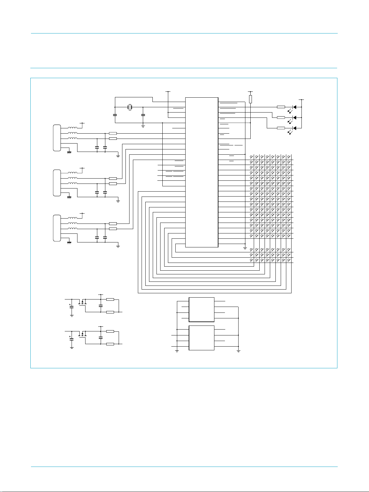
Philips Semiconductors
17. Application information
ISP1130
USB compound hub with keyboard controller
handbook, full pagewidth
J1
L7
1
L1
2
L2
3
4
5
upstream
port
J2
L8
1
L3
2
L4
3
4
5
downstream
port 1
J3
L9
1
L5
2
L6
3
4
5
downstream
port 2
V
CC
XTAL1
XTAL1
6 MHz
C1
R8 22 Ω
R9 22 Ω
C4
47 pF
R10 22 Ω
R11 22 Ω
C6
47 pF
R12 22 Ω
R13 22 Ω
C8
47 pF
22 pF
V
CC
UP_1
UP_2
C3
47 pF
V
CC1
DN_1
DN_2
C5
47 pF
V
CC2
DN_3
DN_4
C7
47 pF
C2
22 pF
PSW1
PSW2
V
V
CC1
CC2
OC1/DPGL1
OC2/DPGL2
XTAL2
RESET
V
CC
GND
V
pu(3.3)
UP_DM
UP_DP
DN1_DM
DN1_DP
DN2_DM
DN2_DP
PSW1
PSW2
GND
MX0
MX1
MX2
MX3/SCL
MX4/SDA
MX5
MX6
MX7
MY0
MY1
MY2
10
11
12
13
14
15
16
17
18
19
1
2
3
4
5
6
7
8
9
20
21
22
23
24
25
26
27
28
U1
ISP1130
GND
56
CAPSLOCK
55
NUMLOCK
54
SCRLOCK
53
INT
52
PSEN
51
ALE
50
EA
49
SYNCLK
48
MEMSEL/UPGL
47
GND
46
MY17/WR
45
MY16/RD
44
MY15
43
MY14
42
MY13
41
MY12
40
MY11
39
MY10
38
MY9
37
MY8
36
MY7
35
MY6
34
MY5
33
MY4
32
MY3
31
V
reg(3.3)
30
GND
29
V
CC
V
R14
4.7 kΩ
R3
470 Ω
R4
470 Ω
R5
470 Ω
CC
D3
Scroll
Lock
D2
Num
Lock
D1
Caps
Lock
V
0.1 µF
C10
0.1 µF
CC
R6
100 kΩ
C9
R1
PSW1
47 kΩ
V
CC
R7
100 kΩ
R2
47 kΩ
PSW2
DN_3
DN_4
GND
GND
GND
GND
A
1
C
2
U2
SN75240
3
D
4
1
C
2
U3
SN75240
3
D
4
UP_1
8
GND
7
B
6
UP_2
GND
5
A
DN_1
8
GND
7
B
6
DN_2
GND
5
MGS809
V
V
CC1
4.7 µF
CC2
4.7 µF
C11
C12
Q1
PHP125
Q2
PHP125
Fig 12. Typical application circuit.
9397 750 06895
Objective specification Rev. 01 — 23 March 2000 58 of 68
© Philips Electronics N.V. 2000. All rights reserved.
Page 59
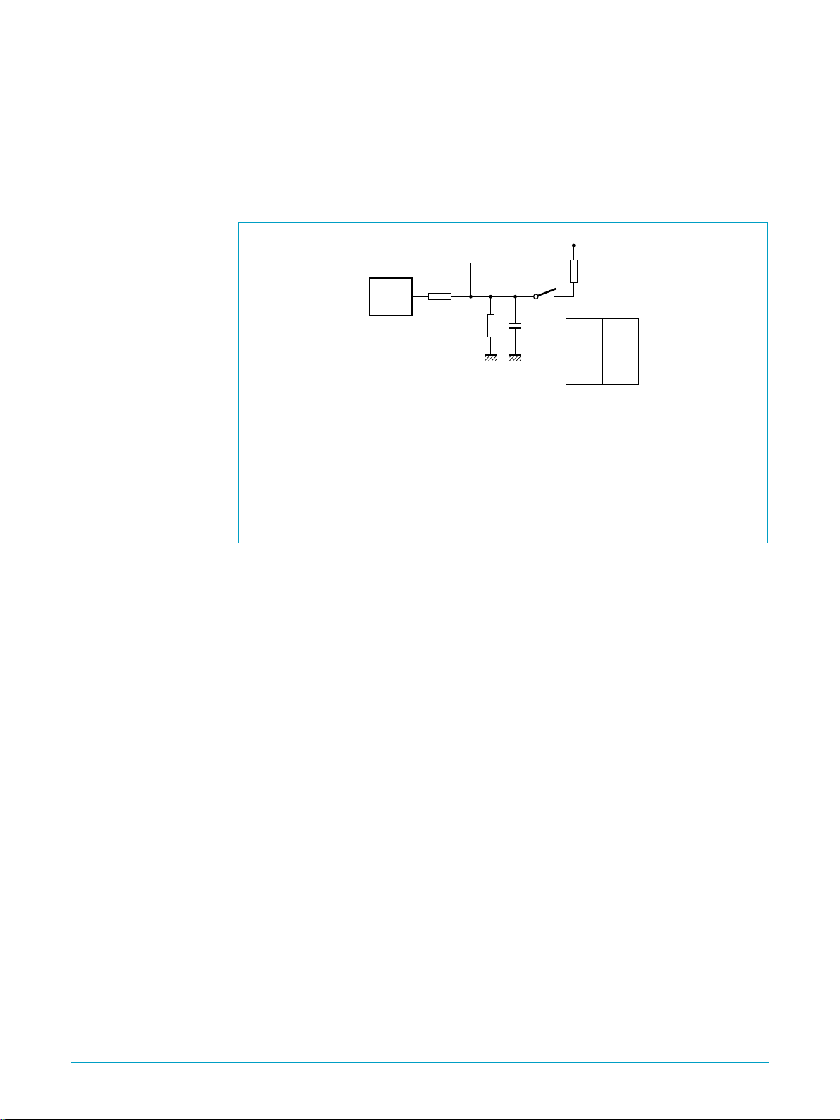
Philips Semiconductors
18. Test information
The dynamic characteristics of the analog I/O ports (D+ and D−) as listed in
Section 16, were determined using the circuit shown in Figure 13.
ISP1130
USB compound hub with keyboard controller
handbook, halfpage
D.U.T.
18 Ω
test point
15 kΩ
S1
C
L
Load capacitance:
CL= 50 pF (full-speed mode)
CL= 200 pF or 600 pF (low-speed mode, minimum or maximum timing).
Speed selection:
full-speed mode (FS): 1.5 kΩ pull-up resistor on D+
low-speed mode (LS): 1.5 kΩ pull-up resistor on D−.
Fig 13. Load impedance for D+ and D− pins.
V
1.5 kΩ
test
D−/LS
D+/LS
D−/FS
D+/FS
CC
S1
closed
open
open
closed
MGS802
9397 750 06895
© Philips Electronics N.V. 2000. All rights reserved.
Objective specification Rev. 01 — 23 March 2000 59 of 68
Page 60
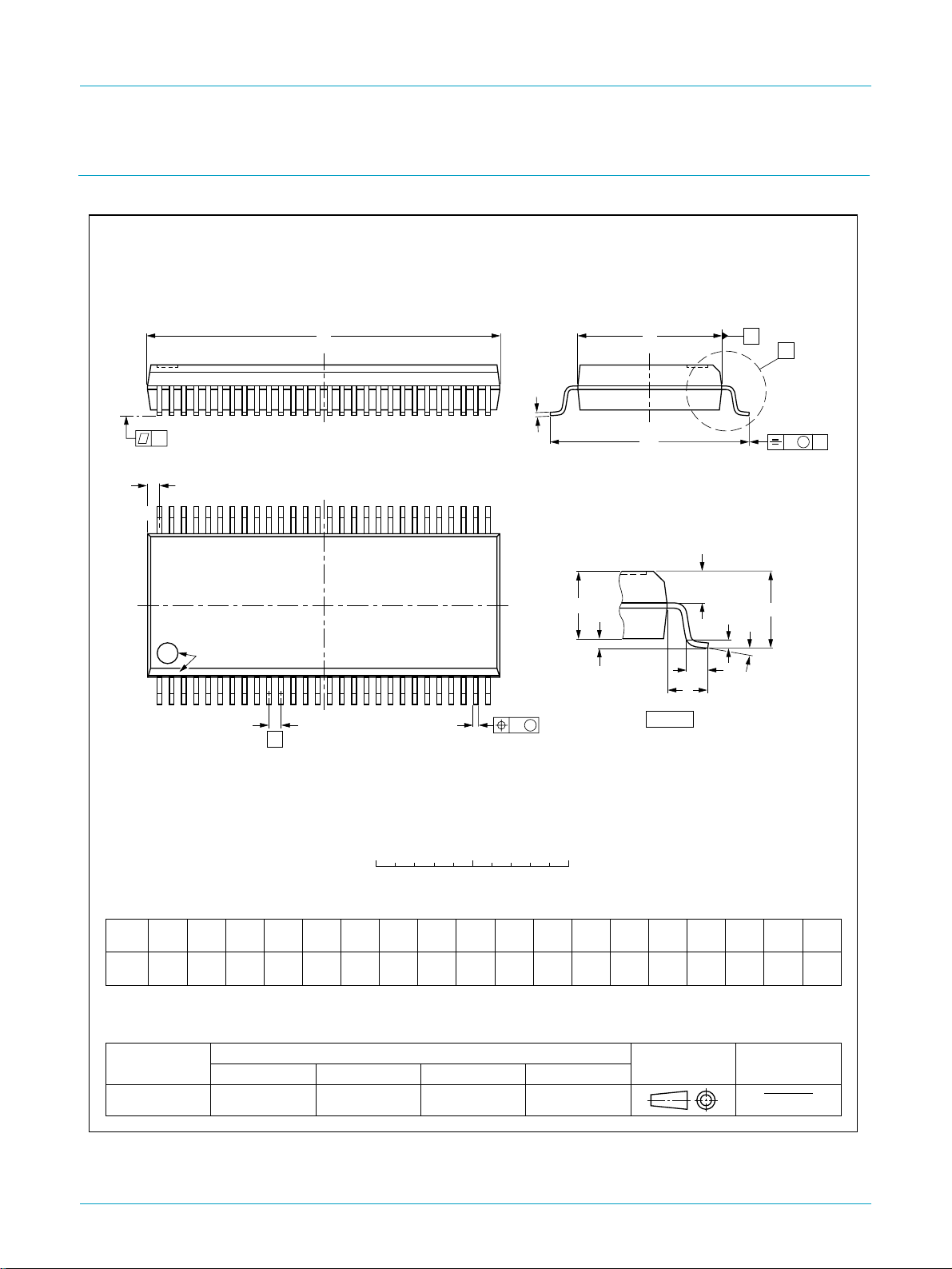
Philips Semiconductors
19. Package outline
ISP1130
USB compound hub with keyboard controller
SSOP56: plastic shrink small outline package; 56 leads; body width 7.5 mm
D
c
y
Z
56
pin 1 index
1
e
29
A
2
A
1
28
w M
b
p
E
H
E
detail X
SOT371-1
A
X
v M
A
Q
A
(A )
3
θ
L
p
L
0 5 10 mm
scale
DIMENSIONS (mm are the original dimensions)
mm
OUTLINE
VERSION
SOT371-1
A
max.
2.8
0.4
0.2
p
2.35
2.20
IEC JEDEC EIAJ
0.25
0.3
0.2
0.22
0.13
MO-118
UNIT A1A2A3b
Note
1. Plastic or metal protrusions of 0.25 mm maximum per side are not included.
(1)E(1)
cD
18.55
18.30
REFERENCES
eHELLpQZywv θ
7.6
7.4
0.635
10.4
10.1
1.0
0.6
1.2
1.0
EUROPEAN
PROJECTION
0.180.251.4 0.1
(1)
0.85
0.40
ISSUE DATE
95-02-04
99-12-27
o
8
o
0
Fig 14. SSOP56 package outline.
9397 750 06895
Objective specification Rev. 01 — 23 March 2000 60 of 68
© Philips Electronics N.V. 2000. All rights reserved.
Page 61
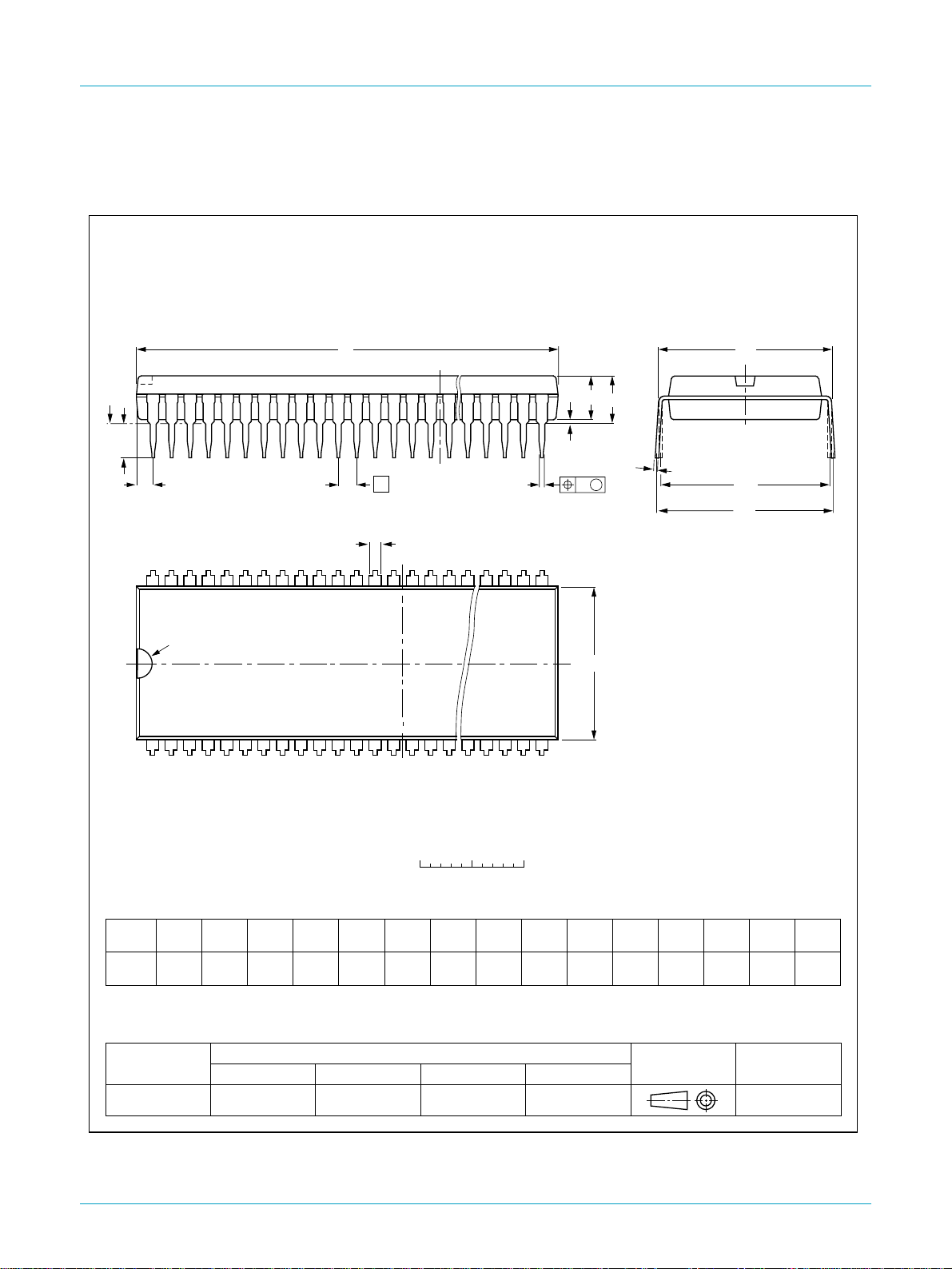
Philips Semiconductors
ISP1130
USB compound hub with keyboard controller
SDIP56: plastic shrink dual in-line package; 56 leads (600 mil)
D
seating plane
L
Z
56
pin 1 index
e
b
SOT400-1
M
E
A
2
A
A
1
w M
b
1
29
E
c
(e )
M
1
H
1
0 5 10 mm
scale
DIMENSIONS (mm are the original dimensions)
A
A
A
UNIT b
Note
1. Plastic or metal protrusions of 0.25 mm maximum per side are not included.
mm
OUTLINE
VERSION
SOT400-1
max.
5.08
12
min.
max.
0.51
4.0
IEC JEDEC EIAJ
1.3
0.8
b
1
0.53
0.40
REFERENCES
cEe M
0.32
0.23
(1) (1)
D
52.4
51.6
14.0
13.6
28
(1)
Z
1
L
M
E
3.2
15.80
2.8
15.24
EUROPEAN
PROJECTION
17.15
15.90
e
w
H
0.181.778 15.24
ISSUE DATE
95-12-06
max.
2.3
Fig 15. SDIP56 package outline.
9397 750 06895
Objective specification Rev. 01 — 23 March 2000 61 of 68
© Philips Electronics N.V. 2000. All rights reserved.
Page 62

Philips Semiconductors
20. Soldering
20.1 Introduction
This text gives a very brief insight to a complex technology. A more in-depth account
of soldering ICs can be found in our
Packages
There is no soldering method that is ideal for all IC packages. Wave soldering is often
preferred when through-hole and surface mount components are mixed on one
printed-circuit board. However, wave soldering is not always suitable for surface
mount ICs, or for printed-circuit boards with high population densities. In these
situations reflow soldering is often used.
20.2 Surface mount packages
20.2.1 Reflow soldering
Reflow soldering requires solder paste (a suspension of fine solder particles, flux and
binding agent) to be applied to the printed-circuit board by screen printing, stencilling
or pressure-syringe dispensing before package placement.
ISP1130
USB compound hub with keyboard controller
Data Handbook IC26; Integrated Circuit
(document order number 9398 652 90011).
Several methods exist for reflowing; for example, infrared/convection heating in a
conveyor type oven. Throughput times (preheating, soldering and cooling) vary
between 100 and 200 seconds depending on heating method.
Typical reflow peak temperatures range from 215 to 250 °C. The top-surface
temperature of the packages should preferable be kept below 230 °C.
20.2.2 Wave soldering
Conventional single wave soldering is not recommended for surface mount devices
(SMDs) or printed-circuit boards with a high component density, as solder bridging
and non-wetting can present major problems.
To overcome these problems the double-wave soldering method was specifically
developed.
If wave soldering is used the following conditions must be observed for optimal
results:
Use a double-wave soldering method comprising a turbulent wave with high
•
upward pressure followed by a smooth laminar wave.
For packages with leads on two sides and a pitch (e):
•
– larger than or equal to 1.27 mm, the footprint longitudinal axis is preferred to be
parallel to the transport direction of the printed-circuit board;
– smaller than 1.27 mm, the footprint longitudinal axis must be parallel to the
transport direction of the printed-circuit board.
The footprint must incorporate solder thieves at the downstream end.
For packages with leads on four sides, the footprint must be placed at a 45° angle
•
to the transport direction of the printed-circuit board. The footprint must
incorporate solder thieves downstream and at the side corners.
9397 750 06895
Objective specification Rev. 01 — 23 March 2000 62 of 68
© Philips Electronics N.V. 2000. All rights reserved.
Page 63

Philips Semiconductors
During placement and before soldering, the package must be fixed with a droplet of
adhesive. The adhesive can be applied by screen printing, pin transfer or syringe
dispensing. The package can be soldered after the adhesive is cured.
Typical dwell time is 4 seconds at 250 °C. A mildly-activated flux will eliminate the
need for removal of corrosive residues in most applications.
20.2.3 Manual soldering
Fix the component by first soldering two diagonally-opposite end leads. Use a low
voltage (24 V or less) soldering iron applied to the flat part of the lead. Contact time
must be limited to 10 seconds at up to 300 °C.
When using a dedicated tool, all other leads can be soldered in one operation within
2 to 5 seconds between 270 and 320 °C.
20.3 Through-hole mount packages
20.3.1 Soldering by dipping or by solder wave
The maximum permissible temperature of the solder is 260 °C; solder at this
temperature must not be in contact with the joints for more than 5 seconds. The total
contact time of successive solder waves must not exceed 5 seconds.
ISP1130
USB compound hub with keyboard controller
The device may be mounted up to the seating plane, but the temperature of the
plastic body must not exceed the specified maximum storage temperature (T
If the printed-circuit board has been pre-heated, forced cooling may be necessary
immediately after soldering to keep the temperature within the permissible limit.
20.3.2 Manual soldering
Apply the soldering iron (24 V or less) to the lead(s) of the package, either below the
seating plane or not more than 2 mm above it. If the temperature of the soldering iron
bit is less than 300 °C it may remain in contact for up to 10 seconds. If the bit
temperature is between 300 and 400 °C, contact may be up to 5 seconds.
stg(max)
).
9397 750 06895
Objective specification Rev. 01 — 23 March 2000 63 of 68
© Philips Electronics N.V. 2000. All rights reserved.
Page 64

Philips Semiconductors
20.4 Package related soldering information
Table 93: Suitability of IC packages for wave, reflow and dipping soldering methods
Mounting Package Soldering method
Through-hole
mount
Surface mount BGA, LFBGA, SQFP,
[1] All surface mount (SMD) packages are moisture sensitive. Depending upon the moisture content, the
[2] For SDIP packages, the longitudinal axis must be parallel to the transport direction of the
[3] These packages are not suitable for wave soldering as a solder joint between the printed-circuit board
[4] If wave soldering is considered, then the package must be placed at a 45° angle to the solder wave
[5] Wave soldering is only suitable for LQFP, QFP and TQFP packages with a pitch (e) equal to or larger
[6] Wave soldering is only suitable for SSOP and TSSOP packages with a pitch(e) equal to or larger than
ISP1130
USB compound hub with keyboard controller
Wave Reflow
DBS, DIP, HDIP, SDIP, SIL suitable
[2]
− suitable
not suitable suitable −
TFBGA
HBCC, HLQFP, HSQFP,
not suitable
[3]
suitable −
HSOP, HTQFP, HTSSOP,
SMS
[4]
PLCC
LQFP, QFP, TQFP not recommended
SSOP, TSSOP, VSO not recommended
maximum temperature (with respect to time) and body size of the package,there is a risk that internal
or external package cracks may occur due to vaporization of the moisture in them (the so called
popcorn effect). For details, refer to the Drypack information in the
Circuit Packages; Section: Packing Methods
printed-circuit board.
and heatsink (at bottom version) can not be achieved, and as solder may stick to the heatsink (on top
version).
direction. The package footprint must incorporate solder thieves downstream and at the side corners.
than 0.8 mm; it is definitely not suitable for packages with a pitch (e) equal to or smaller than 0.65 mm.
0.65 mm; it is definitely not suitable for packages with a pitch (e) equal to or smaller than 0.5 mm.
, SO, SOJ suitable suitable −
[4] [5]
suitable −
[6]
suitable −
Data Handbook IC26; Integrated
.
[1]
Dipping
9397 750 06895
Objective specification Rev. 01 — 23 March 2000 64 of 68
© Philips Electronics N.V. 2000. All rights reserved.
Page 65

Philips Semiconductors
21. Revision history
Table 94: Revision history
Rev Date CPCN Description
01 20000323 Objective specification; initial version.
ISP1130
USB compound hub with keyboard controller
9397 750 06895
Objective specification Rev. 01 — 23 March 2000 65 of 68
© Philips Electronics N.V. 2000. All rights reserved.
Page 66

Philips Semiconductors
22. Data sheet status
ISP1130
USB compound hub with keyboard controller
Datasheet status Product status Definition
Objective specification Development This data sheet contains the design target or goal specifications for product development. Specification may
change in any manner without notice.
Preliminary specification Qualification This data sheet contains preliminary data, and supplementary data will be published at a later date. Philips
Semiconductors reserves the right to make changes at any time without notice in order to improve design and
supply the best possible product.
Product specification Production This data sheet contains final specifications. Philips Semiconductors reserves the right to make changes at any
time without notice in order to improve design and supply the best possible product.
[1] Please consult the most recently issued data sheet before initiating or completing a design.
23. Definitions
Short-form specification — The data in a short-form specification is
extracted from a full data sheet with the same type number and title. For
detailed information see the relevant data sheet or data handbook.
Limiting values definition — Limiting values given are in accordance with
the Absolute Maximum Rating System (IEC 60134). Stress above one or
more of the limiting values may cause permanent damage to the device.
These are stress ratings only and operation of the device at these or at any
other conditions above those given in the Characteristics sections of the
specification is not implied. Exposure to limiting values for extended periods
may affect device reliability.
Application information — Applications that are described herein for any
of these products are for illustrative purposes only. Philips Semiconductors
make no representation or warranty that such applications will be suitable for
the specified use without further testing or modification.
24. Disclaimers
Life support — These products are not designed for use in life support
appliances, devices, or systems where malfunction of these products can
reasonably be expected to result in personal injury. Philips Semiconductors
[1]
customers using or selling these products for use in such applications do so
at their own risk and agree to fully indemnify Philips Semiconductors for any
damages resulting from such application.
Right to make changes — Philips Semiconductors reserves the right to
make changes, without notice, in the products, including circuits, standard
cells, and/or software, described or contained herein in order to improve
design and/or performance. Philips Semiconductors assumes no
responsibility or liability for the use of any of these products, conveys no
licence or title under any patent, copyright, or mask work right to these
products, and makes no representations or warranties that these products
are free from patent, copyright, or mask work right infringement, unless
otherwise specified.
25. Licenses
Purchase of Philips I2C components
Purchase of Philips I
under the Philips’ I
2
C system provided the system conforms to the I2C
I
specification defined by Philips. This specification can be
ordered using the code 9398 393 40011.
2
C components conveys a license
2
C patent to use the components in the
26. Trademarks
ACPI — is an open industry specification for PC power management,
co-developed by Intel Corp., Microsoft Corp. and Toshiba
GoodLink — is a trademark of Royal Philips Electronics
OnNow — is a trademark of Microsoft Corp.
9397 750 06895
Objective specification Rev. 01 — 23 March 2000 66 of 68
SMBus — is a bus specification for PC power management, developed by
Intel Corp. based on the I
SoftConnect — is a trademark of Royal Philips Electronics
2
C-bus from Royal Philips Electronics
© Philips Electronics N.V. 2000 All rights reserved.
Page 67

Philips Semiconductors
USB compound hub with keyboard controller
Philips Semiconductors - a worldwide company
ISP1130
Argentina: see South America
Australia: Tel. +61 2 9704 8141, Fax. +61 2 9704 8139
Austria: Tel. +43 160 101, Fax. +43 160 101 1210
Belarus: Tel. +375 17 220 0733, Fax. +375 17 220 0773
Belgium: see The Netherlands
Brazil: see South America
Bulgaria: Tel. +359 268 9211, Fax. +359 268 9102
Canada: Tel. +1 800 234 7381
China/Hong Kong: Tel. +852 2 319 7888, Fax. +852 2 319 7700
Colombia: see South America
Czech Republic: see Austria
Denmark: Tel. +45 3 288 2636, Fax. +45 3 157 0044
Finland: Tel. +358 961 5800, Fax. +358 96 158 0920
France: Tel. +33 14 099 6161, Fax. +33 14 099 6427
Germany: Tel. +49 40 23 5360, Fax. +49 402 353 6300
Hungary: see Austria
India: Tel. +91 22 493 8541, Fax. +91 22 493 8722
Indonesia: see Singapore
Ireland: Tel. +353 17 64 0000, Fax. +353 17 64 0200
Israel: Tel. +972 36 45 0444, Fax. +972 36 49 1007
Italy: Tel. +39 039 203 6838, Fax +39 039 203 6800
Japan: Tel. +81 33 740 5130, Fax. +81 3 3740 5057
Korea: Tel. +82 27 09 1412, Fax. +82 27 09 1415
Malaysia: Tel. +60 37 50 5214, Fax. +60 37 57 4880
Mexico: Tel. +9-5 800 234 7381
Middle East: see Italy
Netherlands: Tel. +31 40 278 2785, Fax. +31 40 278 8399
New Zealand: Tel. +64 98 49 4160, Fax. +64 98 49 7811
Norway: Tel. +47 22 74 8000, Fax. +47 22 74 8341
Philippines: Tel. +63 28 16 6380, Fax. +63 28 17 3474
Poland: Tel. +48 22 5710 000, Fax. +48 22 5710 001
Portugal: see Spain
Romania: see Italy
Russia: Tel. +7 095 755 6918, Fax. +7 095 755 6919
Singapore: Tel. +65 350 2538, Fax. +65 251 6500
Slovakia: see Austria
Slovenia: see Italy
South Africa: Tel. +27 11 471 5401, Fax. +27 11 471 5398
South America: Tel. +55 11 821 2333, Fax. +55 11 829 1849
Spain: Tel. +34 33 01 6312, Fax. +34 33 01 4107
Sweden: Tel. +46 86 32 2000, Fax. +46 86 32 2745
Switzerland: Tel. +41 14 88 2686, Fax. +41 14 81 7730
Taiwan: Tel. +886 22 134 2865, Fax. +886 22 134 2874
Thailand: Tel. +66 27 45 4090, Fax. +66 23 98 0793
Turkey: Tel. +90 216 522 1500, Fax. +90 216 522 1813
Ukraine: Tel. +380 44 264 2776, Fax. +380 44 268 0461
United Kingdom: Tel. +44 208 730 5000, Fax. +44 208 754 8421
United States: Tel. +1 800 234 7381
Uruguay: see South America
Vietnam: see Singapore
Yugoslavia: Tel. +381 11 3341 299, Fax. +381 11 3342 553
For all other countries apply to: Philips Semiconductors,
International Marketing & Sales Communications,
Building BE, P.O. Box 218, 5600 MD EINDHOVEN,
The Netherlands, Fax. +31 40 272 4825
Internet: http://www.semiconductors.philips.com
(SCA69)
9397 750 06895
Objective specification Rev. 01 — 23 March 2000 67 of 68
© Philips Electronics N.V. 2000. All rights reserved.
Page 68

Philips Semiconductors
Contents
ISP1130
USB compound hub with keyboard controller
1 General description . . . . . . . . . . . . . . . . . . . . . . 1
2 Features . . . . . . . . . . . . . . . . . . . . . . . . . . . . . . . 1
3 Ordering information. . . . . . . . . . . . . . . . . . . . . 2
4 Block diagram . . . . . . . . . . . . . . . . . . . . . . . . . . 3
5 Pinning information. . . . . . . . . . . . . . . . . . . . . . 4
5.1 Pinning . . . . . . . . . . . . . . . . . . . . . . . . . . . . . . . 4
5.2 Pin description . . . . . . . . . . . . . . . . . . . . . . . . . 5
6 Functional description . . . . . . . . . . . . . . . . . . . 7
6.1 80C51 microcontroller. . . . . . . . . . . . . . . . . . . . 8
6.2 Analog transceivers . . . . . . . . . . . . . . . . . . . . . 8
6.3 Philips Serial Interface Engine (SIE). . . . . . . . . 8
6.4 Hub repeater. . . . . . . . . . . . . . . . . . . . . . . . . . . 8
6.5 End-of-frame timers . . . . . . . . . . . . . . . . . . . . . 8
6.6 General and individual port controller. . . . . . . . 8
6.7 GoodLink . . . . . . . . . . . . . . . . . . . . . . . . . . . . . 9
6.8 SoftConnect . . . . . . . . . . . . . . . . . . . . . . . . . . . 9
6.9 Bit clock recovery . . . . . . . . . . . . . . . . . . . . . . 10
6.10 Voltage regulator . . . . . . . . . . . . . . . . . . . . . . 10
6.11 PLL clock multiplier. . . . . . . . . . . . . . . . . . . . . 10
6.12 Overcurrent detection . . . . . . . . . . . . . . . . . . . 10
6.13 Power-on reset . . . . . . . . . . . . . . . . . . . . . . . . 10
6.14 I
2
C-bus interface. . . . . . . . . . . . . . . . . . . . . . . 10
7 Endpoint descriptions. . . . . . . . . . . . . . . . . . . 11
7.1 Endpoint configuration . . . . . . . . . . . . . . . . . . 11
7.2 Hub endpoint 0 (control). . . . . . . . . . . . . . . . . 12
7.3 Hub endpoint 1 (interrupt). . . . . . . . . . . . . . . . 12
8 Host requests. . . . . . . . . . . . . . . . . . . . . . . . . . 13
8.1 Standard requests . . . . . . . . . . . . . . . . . . . . . 13
8.2 Hub specific requests . . . . . . . . . . . . . . . . . . . 14
8.3 Descriptors . . . . . . . . . . . . . . . . . . . . . . . . . . . 16
8.4 Hub responses . . . . . . . . . . . . . . . . . . . . . . . . 19
9 Commands . . . . . . . . . . . . . . . . . . . . . . . . . . . . 22
9.1 Initialization commands . . . . . . . . . . . . . . . . . 24
9.2 Data flow commands . . . . . . . . . . . . . . . . . . . 25
9.3 General commands . . . . . . . . . . . . . . . . . . . . 30
10 Keyboard controller. . . . . . . . . . . . . . . . . . . . . 34
10.1 Microcontroller core . . . . . . . . . . . . . . . . . . . . 34
10.2 Memory map. . . . . . . . . . . . . . . . . . . . . . . . . . 34
10.3 Special function registers (SFRs) . . . . . . . . . . 35
10.4 Hub control registers. . . . . . . . . . . . . . . . . . . . 39
10.5 Interrupt structure . . . . . . . . . . . . . . . . . . . . . . 39
10.6 Timers/counters . . . . . . . . . . . . . . . . . . . . . . . 40
10.7 Watchdog timer. . . . . . . . . . . . . . . . . . . . . . . . 42
10.8 I/O description. . . . . . . . . . . . . . . . . . . . . . . . . 44
10.9 I/O port mapping. . . . . . . . . . . . . . . . . . . . . . . 44
10.10 Keyboard matrix implementation . . . . . . . . . . 44
10.11 Suspend and resume . . . . . . . . . . . . . . . . . . . 45
11 I
2
C-bus interface. . . . . . . . . . . . . . . . . . . . . . . . 46
11.1 Protocol. . . . . . . . . . . . . . . . . . . . . . . . . . . . . . 47
11.2 Hardware connections . . . . . . . . . . . . . . . . . . 47
11.3 Data transfer . . . . . . . . . . . . . . . . . . . . . . . . . . 48
12 Hub power modes . . . . . . . . . . . . . . . . . . . . . . 52
12.1 Voltage drop requirements . . . . . . . . . . . . . . . 52
13 Overcurrent detection . . . . . . . . . . . . . . . . . . . 53
13.1 Overcurrent circuit description . . . . . . . . . . . . 53
13.2 Power switch selection . . . . . . . . . . . . . . . . . . 53
13.3 Tuning the overcurrent trip voltage . . . . . . . . . 53
13.4 Reference circuit. . . . . . . . . . . . . . . . . . . . . . . 54
14 Limiting values. . . . . . . . . . . . . . . . . . . . . . . . . 55
15 Static characteristics. . . . . . . . . . . . . . . . . . . . 56
16 Dynamic characteristics . . . . . . . . . . . . . . . . . 57
17 Application information. . . . . . . . . . . . . . . . . . 58
18 Test information. . . . . . . . . . . . . . . . . . . . . . . . 59
19 Package outline . . . . . . . . . . . . . . . . . . . . . . . . 60
20 Soldering. . . . . . . . . . . . . . . . . . . . . . . . . . . . . . 62
20.1 Introduction . . . . . . . . . . . . . . . . . . . . . . . . . . 62
20.2 Surface mount packages . . . . . . . . . . . . . . . . 62
20.3 Through-hole mount packages . . . . . . . . . . . . 63
20.4 Package related soldering information . . . . . . 64
21 Revision history . . . . . . . . . . . . . . . . . . . . . . . . 65
22 Data sheet status . . . . . . . . . . . . . . . . . . . . . . . 66
23 Definitions. . . . . . . . . . . . . . . . . . . . . . . . . . . . . 66
24 Disclaimers. . . . . . . . . . . . . . . . . . . . . . . . . . . . 66
25 Licenses . . . . . . . . . . . . . . . . . . . . . . . . . . . . . . 66
26 Trademarks. . . . . . . . . . . . . . . . . . . . . . . . . . . . 66
© Philips Electronics N.V. 2000. Printed in The Netherlands
All rights are reserved. Reproduction in whole or in part is prohibited without the prior
written consent of the copyright owner.
The information presented in this document does not form part of any quotation or
contract, is believed to be accurate and reliable and may be changed without notice. No
liability will be accepted by the publisher for any consequence of its use. Publication
thereof does not convey nor imply any license under patent- or other industrial or
intellectual property rights.
Date of release: 23 March 2000 Document order number: 9397 750 06895
 Loading...