

Page 1

ISP1581
Universal Serial Bus 2.0 high-speed interface device
Rev. 02 — 23 October 2000 Objective specification
1. General description
The ISP1581 is a cost-optimized and feature-optimized Universal Serial Bus (USB)
interface device, which fully complies with the
Rev. 2.0
microcontroller or microprocessor. The ISP1581 communicates with the system’s
microcontroller/processor through a high-speed general-purpose parallel interface.
The ISP1581 supports automatic detection of USB 2.0 system operation. The
USB 1.1 fall-back mode allows the device to remain operational under full-speed
conditions. It is designed as a generic USB interface device so that it can fit into all
existing device classes, such as: Imaging Class, Mass Storage Devices,
Communication Devices, Printing Devices and Human Interface Devices.
Universal Serial Bus Specification
. It provideshigh-speedUSB communication capacity to systems based on a
The internal generic DMA block allows easy integration into data streaming
applications. In addition, the various configurations of the DMA block are tailored for
mass storage applications.
The modular approach to implementing a USB interface device allows the designer to
select the optimum system microcontroller from the wide variety available. The ability
to re-use existing architecture and firmware investments shortens the development
c
c
time, eliminates risk and reduces costs. The result is fast and efficient developmentof
the most cost-effective USB peripheral solution.
The ISP1581 is ideally suited for many types of peripherals, such as: printers;
scanners; magneto-optical (MO), compact disc (CD), digital video disc (DVD) and
Zip®/Jaz® drives; digital still cameras; USB-to-Ethernet links; cable and DSL
modems. The low power consumption during ‘suspend’ mode allows easy design of
equipment that is compliant to the ACPI™, OnNow™ and USB power management
requirements.
The ISP1581 also incorporates features such as SoftConnect™, a reduced
frequency crystal oscillator and integrated termination resistors. These features allow
significant cost savings in system design and easy implementation of advanced USB
functionality into PC peripherals.
Page 2

Philips Semiconductors
2. Features
■ Complies fully with Universal Serial Bus Specification Rev. 2.0
■ Complies with most Device Class specifications
■ High performance USB interface device with integrated Serial Interface Engine
■ Supports automatic USB 2.0 mode detection and USB 1.1 fall-back mode
■ High speed DMA interface
■ Fully autonomous and multi-configuration DMA operation
■ Up to 14 programmable USB endpoints with 2 fixed control IN/OUT endpoints
■ Integrated physical 8 kbyte of multi-configuration FIFO memory
■ Endpoints with double buffering to increase throughput and ease real-time data
■ Bus independent interface with most microcontroller/microprocessors
■ Bus-powered capability with low power consumption and low ‘suspend’ current
■ 12 MHz crystal oscillator with integrated PLL for low EMI
■ Software controlled connection to the USB bus (SoftConnect™)
■ Complies with the ACPI™, OnNow™ and USB power management requirements
■ Internal power-on and low-voltage reset circuit, also supporting a software reset
■ Operation over the extended USB bus voltage range (4.0 to 5.5 V) with 5 V
■ Operating temperature range −40 to +85 °C
■ 12 kV in-circuit ESD protection on human accessible pins such as D+ and D−
■ Full-scan design with high fault coverage (>99%)
■ Available in LQFP64 package.
ISP1581
USB 2.0 HS interface device
(SIE), FIFO memory, data transceiver and 3.3 V voltage regulators
transfer
(16 Mbytes/s or 16 Mwords/s)
tolerant I/O pads
3. Applications
■ Personal digital assistant (PDA)
■ Mass storage device, e.g., Zip®, Jaz®, MO, CD, DVD drive
■ Digital camera
■ Communication device, e.g. router, modem
■ Printer
■ Scanner.
4. Ordering information
Table 1: Ordering information
Type number Package
Name Description Version
ISP1581BD LQFP64 Plastic low profile quad flat package; 64 leads; body 10 x 10 x 1.4 mm SOT314-2
9397 750 07648
Objective specification Rev. 02 — 23 October 2000 2 of 73
© Philips Electronics N.V. 2000. All rights reserved.
Page 3
9397 750 07648
Objective specification Rev. 02 — 23 October 2000 3 of 73
5. Block diagram
Philips Semiconductors
to/from USB
D−
D+
5
6
3.3 V
1.5
kΩ
12.2 kΩ
(±0.1%)
RESET
V
CC(5.0)
© Philips Electronics N.V. 2000. All rights reserved.
RPU
RREF
4
7
8
10
2, 37,
43, 64
5 V
1, 36, 42, 61
TRANSCEIVER
POWER-ON
VOLTAGE
REGULATORS
DGND
USB 2.0
RESET
4
SoftConnect
2 2
AGND
3.3 V
3.3 V
V
reg(3.3)
43, 23
V
CC(3.3)
internal
reset
digital
supply
analog
supply
24, 58
12 MHz
XTAL2XTAL1
60 59
40× PLL
OSCILLATOR
BIT CLOCK
RECOVERY
PHILIPS
SIE
SYSTEM
CONTROLLER
63
SUSPEND62WAKEUP
MEMORY
MANAGEMENT
UNIT
INTEGRATED
RAM
(8 KBYTE)
DMA
HANDLER
DMA
REGISTERS
MICRO-
CONTROLLER
HANDLER
ISP1581
Denotes shared pin usage
*
CS0, CS1,
DA0
*
18, 17,
19, 20, 21
, DA1*, DA2
DREQ, DACK,
DIOR, DIOW
5 4
DMA
INTERFACE
MICRO
CONTROLLER
INTERFACE
12, 13,
14, 15
40, 41,
44 to 57
20, 9
38, 39, 30 to 35
25, 29, 26, 27
MGT234
11
16
22
19
22
28
EOT
INTRQ
IORDY
16
DATA0 to DATA15
BUS_CONF
2
MODE0
READY
8
AD0 to AD7
4
CS, ALE/A0, (R/W)/RD,
DS/WR
INT
*
, MODE1
*
*
*
USB 2.0 HS interface device
The direction of pins DREQ, DACK, DIOR and DIOW is determined by bit MASTER (DMA Hardware register) and bit ATA_MODE(DMA Configuration register).
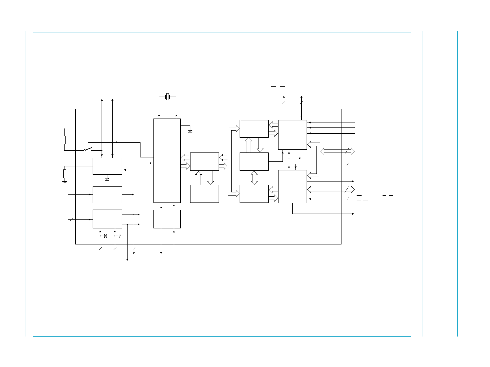
Fig 1. Block diagram.
ISP1581
Page 4
Philips Semiconductors
6. Pinning information
6.1 Pinning
dth
ISP1581
USB 2.0 HS interface device
CC(5.0)
V
SUSPEND
WAKEUP
DGND
XTAL1
64
63
62
61
60
1
DGND
V
CC(5.0)
V
reg(3.3)
MODE1
2
AGND
3
4
D−
5
6
D+
RPU
7
RREF
8
9
RESET
10
EOT
11
DREQ
12
DACK
13
DIOR
14
DIOW
15
INTRQ 33
16
CC(3.3)
XTAL2
V
59
58
ISP1581BD
DATA15
DATA14
57
56
DATA13
DATA12
55
54
DATA11
DATA10
53
52
DATA9
51
DATA8
50
DATA7
48
47
46
45
44
43
42
41
40
39
38
37
36
35
34
DATA6
DATA5
DATA4
DATA3
DATA2
V
CC(5.0)
DGND
DATA1
DATA0
AD7
AD6
V
CC(5.0)
DGND
AD5
AD4
AD3
17
CS1
18
CS0
19
BUS_CONF/DA0
20
MODE0/DA1
DA2
22
READY/IORDY
23
AGND
24
CC(3.3)
V
25
CS
26
27
DS/WR
(R/W)/RD
28
INT
29
ALE/A0
30
AD0
31
AD1
32
AD2 49
MBL248
21
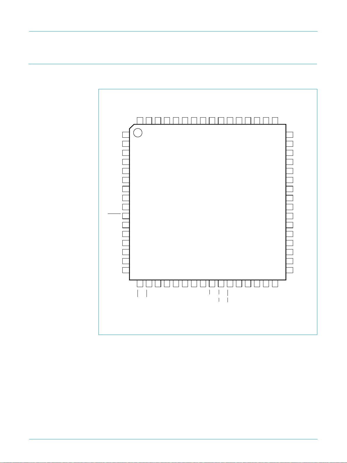
Fig 2. Pin configuration LQFP64.
9397 750 07648
Objective specification Rev. 02 — 23 October 2000 4 of 73
© Philips Electronics N.V. 2000. All rights reserved.
Page 5

Philips Semiconductors
6.2 Pin description
Table 2: Pin description for LQFP64
Symbol
DGND 1 - digital ground
V
CC(5.0)
AGND 3 - analog ground
V
reg(3.3)
D− 5 AI/O USB D− connection (analog)
D+ 6 AI/O USB D+ connection (analog)
RPU 7 AI connection for external pull-up resistor for USB D+ line;
RREF 8 AI connection for external bias resistor; must be connected to
MODE1 9 I selects function of pin ALE/A0 (in Split Bus mode only):
RESET 10 I reset input (Schmitt trigger); a LOW level produces an
EOT 11 I End Of Transfer input (programmable polarity, see
DREQ 12 I/O DMA request (programmable polarity); direction depends
DACK 13 I/O DMA acknowledge (programmable polarity); direction of
DIOR 14 I/O DMA read strobe (programmable polarity); direction
DIOW 15 I/O DMA write strobe (programmable polarity); direction
INTRQ 16 I interrupt request input from ATA/ATAPI peripheral
CS1 17 O chip select output for ATAPI device
CS0 18 O chip select output for ATAPI device
BUS_CONF/
DA0
ISP1581
USB 2.0 HS interface device
[1]
Pin Type
2 - supply voltage (3.3 or 5.0 V)
5 - regulated supply voltage (3.3 V ± 10%) from internal
19 I/O during power-up: input to select the bus configuration
[2]
Description
regulator; supplies internal analog circuits; used to connect
decoupling capacitor and 1.5 kΩ pull-up resistor on D+ line
Remark: Cannot be used to supply external devices.
must be connected to V
via a 1.5 kΩ resistor
reg(3.3)
ground via a 12.2 kΩ (± 0.1%) resistor
0 — ALE function (address latch enable)
1 — A0 function (address/data indicator).
Remark: Connect to V
asynchronous reset; connect to V
in Generic Processor mode.
CC(5.0)
for power-on reset
CC
(internal POR circuit)
Table 37); used in DMA slave mode only
on the bit MASTER in the DMA Hardware register (DMA
master: input, DMA slave: output); see Table 37
depends on bit MASTER in the DMA Hardware register
(DMA slave: input, DMA master: output); see Table 37
depends on bit MASTER in the DMA Hardware register
(DMA slave: input, DMA master: output); see Table 37
depends on bit MASTER in the DMA Hardware register
(DMA slave: input, DMA master: output); see Table 37
0 — Split Bus mode; multiplexed8-bit address/data bus on
AD[7:0], separate 8/16-bit DMA data bus on DATA[15:0]
1 — Generic Processor mode; separate 8-bit address on
AD[7:0], 16-bit DMA data bus on DATA[15:0].
normal operation: address output to select the task file
register of an ATAPI device
9397 750 07648
Objective specification Rev. 02 — 23 October 2000 5 of 73
© Philips Electronics N.V. 2000. All rights reserved.
Page 6

Philips Semiconductors
ISP1581
USB 2.0 HS interface device
Table 2: Pin description for LQFP64
Symbol
[1]
Pin Type
[2]
…continued
Description
MODE0/DA1 20 I/O during power-up: input to select the read/write strobe
functionality in generic processor mode
0 — Motorola style: pin 26 is R/
1 — 8051 style: pin 26 is
W and pin 27 is DS
RD and pin 27 is WR
normal operation: address output to select the task file
register of an ATAPI device
DA2 21 O address output to select the task file register of an ATAPI
device
READY/
IORDY
22 I/O Generic processor mode: ready signal (READY; output)
A LOW level signals that ISP1581 is processing a previous
command or data and is not ready for the next command or
data transfer; a HIGH level signals that ISP1581 is ready
for the next microprocessor read or write.
Split Bus mode: DMA ready signal (IORDY; input); used
for accessing ATAPI peripherals (PIO and UDMA modes
only).
AGND 23 - analog ground
V
CC(3.3)
24 - supply voltage (3.3 V ± 10%); supplies internal digital
circuits
CS 25 I chip select input
W)/RD 26 I input; function is determined by input MODE0 at power-up:
(R/
MODE0 = 0 — pin functions as R/
MODE0 = 1 — pin functions as
W (Motorola style)
RD (8051 style).
DS/WR 27 I input; function is determined by input MODE0 at power-up:
MODE0 = 0 — pin functions as
MODE0 = 1 — pin functions as
DS (Motorola style)
WR (8051 style).
INT 28 O interrupt output; programmable polarity (active HIGH or
LOW) and signaling (edge or level triggered)
ALE/A0 29 I input; function determined by input MODE1 during
power-up:
MODE1 = 0 — address latch enable; a falling edge latches
the address on the multiplexed address/data bus (AD[7:0])
MODE1 = 1 — address/data selection on AD[7:0]; a logic 1
indicates that an address will be written at the next
WR
pulse; a logic 0 indicates that data will be written at the next
WR pulse; used in Split Bus mode only.
AD0 30 I/O bit 0 of multiplexed address/data
AD1 31 I/O bit 1 of multiplexed address/data
AD2 32 I/O bit 2 of multiplexed address/data
AD3 33 I/O bit 3 of multiplexed address/data
AD4 34 I/O bit 4 of multiplexed address/data
AD5 35 I/O bit 5 of multiplexed address/data
DGND 36 - digital ground
V
CC(5.0)
37 - supply voltage (3.3 or 5.0 V)
AD6 38 I/O bit 6 of multiplexed address/data
9397 750 07648
Objective specification Rev. 02 — 23 October 2000 6 of 73
© Philips Electronics N.V. 2000. All rights reserved.
Page 7

Philips Semiconductors
ISP1581
USB 2.0 HS interface device
Table 2: Pin description for LQFP64
CC(5.0)
CC(3.3)
CC(5.0)
[1]
Pin Type
43 - supply voltage (3.3 or 5.0 V)
58 - supply voltage (3.3 V ± 10%); supplies internal digital
64 - supply voltage (3.3 or 5.0 V)
Symbol
AD7 39 I/O bit 7 of multiplexed address/data
DATA0 40 I/O bit 0 of bidirectional data
DATA1 41 I/O bit 1 of bidirectional data
DGND 42 - digital ground
V
DATA2 44 I/O bit 2 of bidirectional data
DATA3 45 I/O bit 3 of bidirectional data
DATA4 46 I/O bit 4 of bidirectional data
DATA5 47 I/O bit 5 of bidirectional data
DATA6 48 I/O bit 6 of bidirectional data
DATA7 49 I/O bit 7 of bidirectional data
DATA8 50 I/O bit 8 of bidirectional data
DATA9 51 I/O bit 9 of bidirectional data
DATA10 52 I/O bit 10 of bidirectional data
DATA11 53 I/O bit 11 of bidirectional data
DATA12 54 I/O bit 12 of bidirectional data
DATA13 55 I/O bit 13 of bidirectional data
DATA14 56 I/O bit 14 of bidirectional data
DATA15 57 I/O bit 15 of bidirectional data
V
XTAL2 59 O crystal oscillator output (12 MHz); connect a fundamental
XTAL1 60 I crystal oscillator input (12 MHz); connect a fundamental
DGND 61 - digital ground
WAKEUP 62 I wake-up input (edge triggered); a LOW-to-HIGH transition
SUSPEND 63 O ’suspend’ state indicator output (4 mA); used as a power
V
[2]
…continued
Description
circuits
parallel-resonant crystal; leavethis pin open when using an
external clock source on pin XTAL1
parallel-resonant crystal or an external clock source
(leaving pin XTAL2 unconnected)
generates a remote wake-up from ‘suspend’ state
switch control output (active LOW) for powered-off
application or as a resume signal to the CPU (active HIGH)
for powered-on application
[1] Symbol names with an overscore (e.g. NAME) represent active LOW signals.
[2] All outputs and I/O pins can source 4 mA of current.
7. Functional description
The ISP1581 is a high-speed USB device controller. It implements the USB 2.0/1.1
physical layer, the packet protocol layer and maintains up to 16 USB endpoints
concurrently (2 control, 14 configurable).
executed by means of external firmware.
9397 750 07648
Objective specification Rev. 02 — 23 October 2000 7 of 73
USB Chapter 9
protocol handling is
© Philips Electronics N.V. 2000. All rights reserved.
Page 8

Philips Semiconductors
The ISP1581 has a fast general-purpose interface for communication with most types
of microcontrollers/processors. This Microcontroller Interface is configured by pins
BUS_CONF, MODE1 and MODE0 to accommodate most interface types. Two bus
configurations are available, selected via input BUS_CONF during power-up:
•
•
ISP1581
USB 2.0 HS interface device
Generic Processor mode (BUS_CONF = 1):
– AD[7:0]: 8-bit address bus (selects target register)
– DATA[15:0]: 16-bit data bus (shared by processor and DMA)
– Control signals: R/W and DS or RD and WR (selected via pin MODE0)
– DMA interface (generic slave mode only): uses lines DATA[15:0] as data bus,
DIOR and DIOW as dedicated read and write strobes.
Split Bus mode (BUS_CONF = 0):
– AD[7:0]: 8-bit local microprocessor bus (multiplexed address/data)
– DATA[15:0]: 16-bit DMA data bus
– Control signals: CS, ALE or A0 (selected via pin MODE1), R/W and DS or RD
and WR (selected via pin MODE0)
– DMA interface (master or slave mode): uses DIOR and DIOW as dedicated read
and write strobes.
For high-bandwidth data transfer, the integrated DMA handler can be invoked to
transfer data to/from external memory or devices. The DMA Interface can be
configured by writing to the proper DMA registers (see Section 9.4).
The ISP1581 supports high-speed USB 2.0 and full-speed USB 1.1 signaling.
Detection of the USB signaling speed is done automatically.
ISP1581 has 8 kbytes of internal FIFO memory, which is shared among the enabled
USB endpoints.
There are 14 configurable data endpoints and 2 control endpoints. Any of the 14 data
endpoints can be separately enabled or disabled. The endpoint type (interrupt,
isochronous or bulk) and packet size of these endpoints can be individually
configured depending on the requirements of the application. Optional double
buffering increases the data throughput of the data endpoints.
The ISP1581 requires a single supply of 3.0 V or 5.0 V, depending on the I/O voltage.
It has 5.0 V tolerant I/O pads and has an internal 3.3 V regulator for powering the
analog transceiver. It supports bus-powered operation with a ‘suspend’ current below
500 µA.
The ISP1581 operates on a 12 MHz crystal oscillator. An integrated 40× PLL clock
multiplier generates the internal sampling clock of 480 MHz.
7.1 USB 2.0 transceiver
The analog transceiver interfaces directly to the USB cable via integrated termination
resistors. The high-speed transceiver requires an external resistor (12.2 kΩ±0.1%)
between pin RREF and ground to ensure an accurate current mirror. A full-speed
transceiver is integrated as well. This makes the ISP1581 compliant with USB 2.0
9397 750 07648
Objective specification Rev. 02 — 23 October 2000 8 of 73
© Philips Electronics N.V. 2000. All rights reserved.
Page 9

Philips Semiconductors
and USB 1.1, supporting both the high-speed and full-speed physical layer. After
automatic speed detection, the Philips Serial Interface Engine sets the transceiver to
use either high-speed or full-speed signaling.
7.2 Philips Serial Interface Engine (SIE)
The Philips SIE implements the full USB protocol layer. It is completely hardwired for
speed and needs no firmware intervention. The functions of this block include:
synchronization pattern recognition, parallel/serial conversion, bit (de-)stuffing, CRC
checking/generation, Packet IDentifier (PID) verification/generation, address
recognition, handshake evaluation/generation.
7.3 Voltage regulators
Two 5 V to 3.3 V voltage regulators are integrated on-chip to separately supply the
analog transceiver and the internal logic. The analog supply voltage is available at pin
V
reg(3.3)
ISP1581
USB 2.0 HS interface device
to supply an external 1.5 kΩ pull-up resistor on the D+ line.
Remark: Pin V
cannot be used to supply external devices.
reg(3.3)
7.4 Memory Management Unit (MMU) and integrated RAM
The MMU and the integrated RAM provide the conversion between the USB speed
(full speed: 12 Mbit/s, high speed: 480 Mbit/s) and the Microcontroller Handler or the
DMA Handler. The data from the USB Bus is stored in the integrated RAM, which is
cleared only when the microcontroller clears the endpoint buffer or when the DMA
Handler has read/written all data from/to the endpoint buffer. A total of 8 kbytes RAM
is available for buffering.
7.5 SoftConnect
The connection to the USB is established by pulling the D+ line (for high-speed
devices) HIGH through a 1.5 kΩ pull-up resistor. In the ISP1581 an external 1.5 kΩ
pull-up resistor must be connected between pins RPU and V
connects the pull-up resistor to the D+ line, when bit SOFTCT in the Mode register is
set (see Table 7). After a hardware reset the pull-up resistor is disconnected by
default (SOFTCT = 0). Bit SOFTCT remains unchanged by a USB bus reset.
. The RPU pin
reg(3.3)
7.6 Bit clock recovery
The bit clock recovery circuit recovers the clock from the incoming USB data stream
using 4× over-sampling principle. It is able to track the jitter and the frequency drift as
specified by the USB specification.
7.7 Multiplying PLL oscillator
A 12 MHz to 480 MHz clock multiplier Phase-Locked Loop (PLL) is integrated
on-chip. This allows the use of a low-cost 12 MHz crystal, which also minimizes EMI.
No external components are needed for the operation of the PLL.
9397 750 07648
Objective specification Rev. 02 — 23 October 2000 9 of 73
© Philips Electronics N.V. 2000. All rights reserved.
Page 10

Philips Semiconductors
7.8 Microcontroller Interface and Microcontroller Handler
The Microcontroller Interface allows direct interfacing to most microcontrollers. The
interface is configured at power-up via inputs BUS_CONF, MODE1 and MODE0.
When BUS_CONF is set to logic 1, the Microcontroller Interface switches to the
Generic Processor mode in which AD[7:0] is the 8-bit address bus and DATA[15:0]
is the separate 16-bit data bus. If BUS_CONF is made logic 0, the interface is in the
Split Bus mode, where AD[7:0] is the local microprocessor bus (multiplexed
address/data) and DATA[15:0] is used as the DMA bus.
If pin MODE0 is set to logic 1, pins RD and WR are the read and write strobes (8051
style). If pin MODE0 is logic 0, pins R/W and DS pins represent the direction and data
strobe (Motorola style).
When pin MODE1 is made logic 0, ALE is used to latch the multiplexed address on
pins AD[7:0]. If pin MODE1 is set to logic 1, A0 is used to indicate address or data.
Pin MODE1 is only used in Split Bus mode: in Generic Processor mode it must be
tied to V
The Microcontroller Handler allows the external microcontroller to access the register
set in the Philips SIE as well as the DMA Handler. The initialization of the DMA
configuration is done via the Microcontroller Handler.
CC(5.0)
ISP1581
USB 2.0 HS interface device
(logic 1).
7.9 DMA Interface and DMA Handler
The DMA block can be subdivided into two blocks: the DMA Handler and the DMA
Interface.
The firmware writes to the DMA Command register to start a DMA transfer (see
Table 30). The command opcode determines whether a generic DMA, PIO,MDMA or
UDMA transfer will start. The Handler interfaces to the same FIFO (internal RAM) as
used by the USB core. Upon receiving the DMA Command, the DMA Handler directs
the data from the internal RAM to the external DMA device and vice versa.
The DMA Interface configures the timings and how the DMA data is accessed. Data
can be transferred either using DIOR and DIOW strobes or by the DACK and DREQ
handshakes. The different DMA configurations are set up by writing to the DMA
Configuration register (see Table 35).
For an IDE-based storage interface, the applicable DMA modes are PIO (Parallel
I/O), MDMA (Multiword DMA; ATA), and UDMA (Ultra DMA; ATA).
For a generic DMA interface, the DMA modes that can be used are Generic DMA
(Slave) and MDMA (Master).
7.10 System Controller
The System Controller implements the USB power-down capabilities of the ISP1581.
Two modes are supported during ‘suspend’ state: powered-on and powered-off.
These modes are selected via bit PWROFF in the Mode register (see Table 7).
Registers are protected against data corruption during wake-up following a ‘resume’.
9397 750 07648
Objective specification Rev. 02 — 23 October 2000 10 of 73
© Philips Electronics N.V. 2000. All rights reserved.
Page 11

Philips Semiconductors
USB 2.0 HS interface device
8. Modes of operation
The ISP1581 has two bus configuration modes, selected via pin BUS_CONF/DA0 at
power-up:
Split Bus mode (BUS_CONF = 0): 8-bit multiplexed address/data bus and
•
separate 8-bit/16-bit DMA bus
Generic Processor mode (BUS_CONF = 1); separate 8-bit address and 16-bit
•
data bus
Details of the bus configurations for each mode are given in Table 3. Typical interface
circuits for each mode are given in Section 13 “Application information”.
Table 3: Bus configuration modes
BUS_CONF PIO width DMA width Description
DMAWD = 0 DMAWD = 1
0 AD[7:0] D[7:0] D[15:0] Split Bus mode: multiplexed address/data on pins AD[7:0];
separate 8/16-bit DMA bus on pins DATA[15:0]
1 A[7:0]
D[15:0]
D[7:0] D[15:0] Generic Processor mode: separate 8-bit address on pins
AD[7:0]; 16-bit data (PIO and DMA) on pins DATA[15:0]
ISP1581
9. Register descriptions
Table 4: Register summary
Name Destination Address
(Hex)
Initialization registers
Address device 00 USB device address + enable 1
Mode device 0C power-down options, global interrupt
Interrupt Configuration device 10 interrupt sources, trigger mode, output
Interrupt Enable device 14 interrupt source enabling 4
DMA Configuration DMA controller 38 see DMA registers 2
DMA Hardware DMA controller 3C see DMA registers 1
Data flow registers
Endpoint Index endpoints 2C endpoint selection, data flow direction 1
Control Function endpoint 28 endpoint buffer management 1
Data Port endpoint 20 data access to endpoint FIFO 2
Buffer Length endpoint 1C packet size counter 2
Endpoint MaxPacketSize endpoint 04 maximum packet size 2
Endpoint Type endpoint 08 selects endpoint type: control,
Short Packet endpoint 24 short packet received on OUT endpoint 2
Description Size
enable, SoftConnect
polarity
isochronous, bulk or interrupt
(bytes)
1
1
2
9397 750 07648
Objective specification Rev. 02 — 23 October 2000 11 of 73
© Philips Electronics N.V. 2000. All rights reserved.
Page 12

Philips Semiconductors
ISP1581
USB 2.0 HS interface device
Table 4: Register summary
Name Destination Address
DMA registers
DMA Command DMA controller 30 controls all DMA transfers 1
DMA Transfer Counter DMA controller 34 sets byte count for DMA Transfer 4
DMA Configuration DMA controller 38 (byte 0) sets GDMA configuration (counter enable,
DMA Hardware DMA controller 3C endian type, master/slave selection, signal
1F0 Task File ATAPI peripheral 40 single address word register: byte 0 (lower
1F1Task File ATAPI peripheral 48 IDE device access 1
1F2 Task File ATAPI peripheral 49 IDE device access 1
1F3 Task File ATAPI peripheral 4A IDE device access 1
1F4 Task File ATAPI peripheral 4B IDE device access 1
1F5 Task File ATAPI peripheral 4C IDE device access 1
1F6 Task File ATAPI peripheral 4D IDE device access 1
1F7 Task File ATAPI peripheral 44 IDE device access (write only; reading
3F6 Task File ATAPI peripheral 4E IDE device access 1
3F7 Task File ATAPI peripheral 4F IDE device access 1
DMA Interrupt Reason DMA controller 50 (byte 0) shows reason (source) for DMA interrupt 1
DMA Interrupt Enable DMA controller 54 (byte 0) enables DMA interrupt sources 1
DMA Endpoint DMA controller 58 selects endpoint FIFO, data flow direction 1
DMA Strobe Timing DMA controller 60 strobe duration in UDMA/MDMA mode 1
General registers
Interrupt device 18 shows interrupt sources 4
Chip ID device 70 product ID code and hardware version 3
Frame Number device 74 last successfully received Start Of Frame:
Scratch device 78 allows save/restore of firmware status
Unlock Device device 7C re-enables register access after ‘suspend’ 2
Test Mode PHY 84 direct setting of D+, D− states, loopback
…continued
Description Size
(Hex)
burst length, data strobing, bus width)
39 (byte 1) sets ATA configuration (IORDY enable,
mode selection: ATA/UDMA/MDMA/PIO)
polarity for DACK, DREQ, DIOW, DIOR
byte) is accessed first
returns 00H)
51 (byte 1) 1
55 (byte 1) 1
lower byte (byte 0) is accessed first
during ‘suspend’
mode, internal transceiver test (PHY)
(bytes)
1
1
1
2
1
2
2
1
9397 750 07648
Objective specification Rev. 02 — 23 October 2000 12 of 73
© Philips Electronics N.V. 2000. All rights reserved.
Page 13

Philips Semiconductors
9.1 Register access
Register access depends on the bus width used:
•
•
Endpoint specific registers are indexed via the Endpoint Index register. The target
endpoint must be selected first, before accessing the following registers:
•
•
•
•
•
•
9.2 Initialization registers
ISP1581
USB 2.0 HS interface device
8-bit bus: multi-byte registers are accessed lower byte (LSB) first.
16-bit bus: for single-byte registers the upper byte (MSB) must be ignored.
Buffer Length
Control Function
Data Port
Endpoint MaxPacketsize
Endpoint Type
Short Packet.
9.2.1 Address register (address: 00H)
This register is used to set the USB assigned address and enable the USB device.
Table 5 shows the Address register bit allocation.
The DEVEN and DEVADDR bits will be cleared whenever a bus reset, a power-on
reset or a soft reset occurs.
In response to the standard USB request SET_ADDRESS, the firmware must write
the (enabled) device address to the Address register, followed by sending an empty
packetto the host. The new device address is activated when the host acknowledges
the empty packet.
Table 5: Address register: bit allocation
Bit 7 6 5 4 3 2 1 0
Symbol DEVEN DEVADDR[6:0]
Reset 0 00H
Bus reset 0 00H
Access R/W R/W
Table 6: Endpoint Configuration register: bit description
Bit Symbol Description
7 DEVEN A logic 1 enables the device.
6 to 0 DEVADDR[6:0] This field specifies the USB device address.
9397 750 07648
Objective specification Rev. 02 — 23 October 2000 13 of 73
© Philips Electronics N.V. 2000. All rights reserved.
Page 14

Philips Semiconductors
ISP1581
USB 2.0 HS interface device
9.2.2 Mode register (address: 0CH)
This register consists of 1 byte (bit allocation: see Table 7). In 16-bit bus mode the
upper byte is ignored.
The Mode register controls the resume, suspend and wake-up behaviour, interrupt
activity, soft reset, clock signals and SoftConnect operation. This register also
controls the Power Off mode during ‘suspend’ state.
Table 7: Mode register: bit allocation
Bit 7 6 5 4 3 2 1 0
Symbol CLKAON SNDRSU GOSUSP SFRESET GLINTENA WKUPCS PWROFF SOFTCT
Reset 00000000
Bus reset 0 0 0 0 unchanged 0 unchanged unchanged
Access R/W R/W R/W R/W R/W R/W R/W R/W
Table 8: Mode register: bit description
Bit Symbol Description
7 CLKAON Clock Always On: A logic 1 indicates that the internal clocks
are always running even during ‘suspend’ state. A logic 0
switches off the internal oscillator and PLL, when they are not
needed. During ‘suspend’ state, this bit must be set to logic 0 to
meet the suspend current requirements. The clock is stopped
after a delay of approximately 2 ms, following the setting of bit
GOSUSP.
6 SNDRSU Send Resume: Writing a logic 1 followed by a logic 0 will
generate an upstream ‘resume’ signal of 10 ms duration, after a
5 ms delay.
5 GOSUSP Go Suspend: Writing a logic 1 followed by a logic 0 will activate
‘suspend’ mode.
4 SFRESET Soft Reset: Writing a logic 1 followed by a logic 0 will enable a
software-initiated reset to ISP1581. A soft reset is similar to a
hardware-initiated reset (via the
3 GLINTENA Global Interrupt Enable: A logic 1 enables all interrupts.
Individual interrupts can be masked OFF by clearing the
corresponding bits in the Interrupt Enable register. Bus reset
value: unchanged.
2 WKUPCS Wake-up on Chip Select: A logic 1 enables remote wake-up
via a LOW level on input
1 PWROFF Power Off mode: A logic 1 enables powering-off during
‘suspend’ state. Output SUSPEND is configured as a power
switch control signal for external devices (HIGH during
‘suspend’). Bus reset value: unchanged.
0 SOFTCT SoftConnect: A logic 1 enables the connection of the 1.5 kΩ
pull-up resistor on pin RPU to the D+ line. Bus reset value:
unchanged.
RESET pin).
CS.
9397 750 07648
Objective specification Rev. 02 — 23 October 2000 14 of 73
© Philips Electronics N.V. 2000. All rights reserved.
Page 15

Philips Semiconductors
ISP1581
USB 2.0 HS interface device
9.2.3 Interrupt Configuration register (address: 10H)
This 1-byte register determines the behaviour and polarity of the INT output. The bit
allocation is shown in Table 9. When the USB SIE receives or generates a ACK, NAK
or STALL, it will generate interrupts depending on three Debug mode bit fields:
CDBGMOD[1:0]: interrupts for the Control endpoint 0
•
DDBGMODIN[1:0]: interrupts for the DATA IN endpoints 1 to 7
•
DDBGMODOUT[1:0]: interrupts for the DATA OUT endpoints 1 to 7.
•
The Debug mode settings for CDBGMOD, DDBGMODIN and DDBGMODOUT allow
the user to individually configure when the ISP1581 will send an interrupt to the
external microprocessor. Table 11 lists the available combinations.
Bit INTPOL controls the signal polarity of the INT output (active HIGH or LOW, rising
or falling edge). For level-triggering bit INTLVL must be made logic 0. By setting
INTLVL to logic 1 an interrupt will generate a pulse of 60 ns (edge-triggering).
Table 9: Interrupt Configuration register: bit allocation
Bit 7 6 5 4 3 2 1 0
Symbol CDBGMOD[1:0] DDBGMODIN[1:0] DDBGMODOUT[1:0] INTLVL INTPOL
Reset 03H 03H 03H 0 0
Bus reset 03H 03H 03H unchanged unchanged
Access R/W R/W R/W R/W R/W
Table 10: Interrupt Configuration register: bit description
Bit Symbol Description
7 to 6 CDBGMOD[1:0] Control 0 Debug Mode: values see Table 11
5 to 4 DDBGMODIN[1:0] Data Debug Mode IN: values see Table 11
3 to 2 DDBGMODOUT[1:0] Data Debug Mode OUT: values see Table 11
1 INTLVL Interrupt Level: selects the signaling mode on output
INT (0 = level, 1 = pulsed). In pulsed mode an interrupt
produces a 60 ns pulse. Bus reset value: unchanged.
0 INTPOL Interrupt Polarity: selects signal polarity on output INT
(0 = active LOW, 1 = active HIGH). Bus reset value:
unchanged.
Table 11: Debug mode settings
Value CDBGMOD DDBGMODIN DDBGMODOUT
00H Interrupt on all ACK,
STALL and NAK
01H Interrupt on all ACK and
STALL
1XH Interrupt on all ACK,
STALL and first NAK
[1] First NAK: the first NAK on an IN or OUT token after a previous ACK response.
Interrupt on all ACK
and NAK
Interrupt on ACK Interrupt on ACK, STALL and
Interrupt on all ACK
[1]
and first NAK
[1]
Interrupt on all ACK, STALL,
NYET and NAK
NYET
Interrupt on all ACK, STALL,
NYET and first NAK
[1]
9397 750 07648
Objective specification Rev. 02 — 23 October 2000 15 of 73
© Philips Electronics N.V. 2000. All rights reserved.
Page 16

Philips Semiconductors
9.2.4 Interrupt Enable register (address: 14H)
This register enables/disables individual interrupt sources. The interrupt for each
endpoint can be individually controlled via the associated IEPnRX or IEPnTX bits (‘n’
representing the endpoint number). All interrupts can be globally disabled via bit
GLINTENA in the Mode Register (see Table 7).
An interrupt is generated when the USB SIE receives or generates an ACK, NAK or
STALL on the USB bus. The interrupt generation depends on the Debug mode
settings of bit fields CDBGMOD, DDBGMODIN and DDBGMODOUT.
All data IN transactions use the Transmit buffers (TX), which are handled by the
DDBGMODIN bits. All data OUT transactions go via the Receive buffers (RX), which
are handled by the DDBGMODOUT bits. Transactions on Control endpoint 0 (IN,
OUT and SETUP) are handled by the CDBGMOD bits.
Interrupts caused by events on the USB bus (SOF, Pseudo SOF, suspend, resume,
bus reset, Setup and High Speed Status) can also be controlled individually. A bus
reset disables all enabled interrupts except bit IEBRST (bus reset), which remains
unchanged.
ISP1581
USB 2.0 HS interface device
The Interrupt Enable Register consists of 4 bytes. The bit allocation is given in
Table 12.
Table 12: Interrupt Enable register: bit allocation
Bit 31 30 29 28 27 26 25 24
Symbol reserved reserved reserved reserved reserved reserved IEP7TX IEP7RX
Reset 00000000
Bus Reset 00000000
Access R/W R/W R/W R/W R/W R/W R/W R/W
Bit 23 22 21 20 19 18 17 16
Symbol IEP6TX IEP6RX IEP5TX IEP5RX IEP4TX IEP4RX IEP3TX IEP3RX
Reset 00000000
Bus Reset 00000000
Access R/W R/W R/W R/W R/W R/W R/W R/W
Bit 15 14 13 12 11 10 9 8
Symbol IEP2TX IEP2RX IEP1TX IEP1RX IEP0TX IEP0RX reserved IEP0SETUP
Reset 00000000
Bus Reset 00000000
Access R/W R/W R/W R/W R/W R/W R/W R/W
Bit 7 6 5 4 3 2 1 0
Symbol reserved IEDMA IEHS_STA IERESM IESUSP IEPSOF IESOF IEBRST
Reset 00000000
Bus Reset 0000000unchanged
Access R/W R/W R/W R/W R/W R/W R/W R/W
9397 750 07648
Objective specification Rev. 02 — 23 October 2000 16 of 73
© Philips Electronics N.V. 2000. All rights reserved.
Page 17

Philips Semiconductors
Table 13: Interrupt Enable register: bit description
Bit Symbol Description
31 to 26 - reserved; must write logic 0
25 to 12 IEP7TX to
11 IEP0TX A logic 1 enables interrupt from the Control IN endpoint 0.
10 IEP0RX A logic 1 enables interrupt from the Control OUT endpoint 0.
9 - reserved
8 IEP0SETUP A logic 1 enables the interrupt for the Setup data received on
7 - reserved
6 IEDMA A logic 1 enables interrupt upon DMA status change detection.
5 IEHS_STA A logic 1 enables interrupt upon detection of a High Speed
4 IERESM A logic 1 enables interrupt upon detection of a ‘resume’ state.
3 IESUSP A logic 1 enables interrupt upon detection of a ‘suspend’ state.
2 IEPSOF A logic 1 enables interrupt upon detection of a Pseudo SOF.
1 IESOF A logic 1 enables interrupt upon detection of an SOF.
0 IEBRST A logic 1 enables interrupt upon detection of a bus reset.
ISP1581
USB 2.0 HS interface device
A logic 1 enables interrupt from the indicated endpoint.
IEP1RX
endpoint 0.
Status change.
9.2.5 DMA Configuration register (address: 38H)
See Section 9.4.3.
9.2.6 DMA Hardware register (address: 3CH)
See Section 9.4.4.
9397 750 07648
Objective specification Rev. 02 — 23 October 2000 17 of 73
© Philips Electronics N.V. 2000. All rights reserved.
Page 18

Philips Semiconductors
ISP1581
USB 2.0 HS interface device
9.3 Data flow registers
9.3.1 Endpoint Index register (address: 2CH)
The Endpoint Index register selects a target endpoint for register access by the
microcontroller. The register consists of 1 byte and the bit allocation is shown in
Table 14. The following registers are indexed:
Endpoint MaxPacketsize
•
Endpoint Type
•
Buffer Length
•
Data Port
•
Short Packet
•
Control Function.
•
For example, to access the OUT data buffer of endpoint 1 via the Data Port register,
the Endpoint Index register has to be written first with 02H.
Table 14: Endpoint Index register: bit allocation
Bit 7 6 5 4 3 2 1 0
Symbol reserved reserved EP0SETUP ENDPIDX[3:0] DIR
Reset 0 0 0 00H 0
Bus reset 0 0 0 00H 0
Access R/W R/W R/W R/W R/W
Table 15: Endpoint Index register: bit description
Bit Symbol Description
7 to 6 - reserved
5 EP0SETUP Selects the SETUP buffer for Endpoint 0:
0 — EP0 data buffer
1 — SETUP buffer.
Must be logic 0 for access to other endpoints than Endpoint 0.
4 to 1 ENDPIDX[3:0] Endpoint Index: Selects the target endpoint for register access
of Buffer Length, Control Function, Data Port, Endpoint Type,
MaxPacketSize and Short Packet.
0 DIR Direction bit: Sets the target endpoint as IN or OUT endpoint:
0 — target endpoint refers to OUT (RX) FIFO
1 — target endpoint refers to IN (TX) FIFO.
Table 16: Addressing of Endpoint 0 buffers
Buffer name EP0SETUP ENDPIDX DIR
SETUP 1 00H 0
Data OUT 0 00H 0
Data IN 0 00H 1
9397 750 07648
Objective specification Rev. 02 — 23 October 2000 18 of 73
© Philips Electronics N.V. 2000. All rights reserved.
Page 19

Philips Semiconductors
ISP1581
USB 2.0 HS interface device
9.3.2 Control Function register (address: 28H)
The Control Function register is used to perform the buffer management on the
endpoints. It consists of 1 byte and the bit configuration is given in Table 17.The
register bits can stall, clear or validate any enabled data endpoint. Before accessing
this register, the Endpoint Index register must be written first to specify the target
endpoint.
Table 17: Control Function register: bit allocation
Bit 7 6 5 4 3 2 1 0
[1]
Symbol reserved reserved reserved CLBUF VENDP reserved STATUS
Reset 00000000
Bus reset 00000000
Access R/W R/W R/W R/W R/W R/W R/W R/W
[1] Only applicable for Endpoint 0.
Table 18: Control Function register: bit description
Bit Symbol Description
7 to 5 - reserved.
4 CLBUF Clear Buffer: A logic 1 clears the RX buffer of the indexed
endpoint; the TX buffer is not affected. Before new data can be
received, old data in the buffer must be cleared first.
3 VENDP Validate Endpoint: A logic 1 validates the data in the TX FIFO
of an IN endpoint for sending on the next IN token. The FIFO
byte count is below or equal to the Endpoint MaxPacketSize.
2 - reserved
1 STATUS Status Acknowledge: This bit controls the generation of ACK
or NAK during the status stage of a SETUP packet. It is
automatically cleared upon completion of the status stage and
upon receiving a SETUP token.
0 — sends NAK
1 — sends empty packet following IN token (host-to-device) or
ACK following OUT token (device-to-host).
0 STALL Stall Endpoint: A logic 1 stalls the indexed endpoint. This bit is
not applicable for isochronous transfers.
STALL
9.3.3 Data Port register (address: 20H)
This 2-byte register provides direct access for a microcontroller to the FIFO of the
indexedendpoint. In case of an 8-bit bus the upper byte is not used. The bit allocation
is shown in Table 19.
Device to host (IN endpoint): After each write action an internal counter is
auto-incremented (by 2 for a 16-bit access, by 1 for an 8-bit access) to the next
location in the TX FIFO. When all bytes have been written, the buffer can be validated
via the Control Function register (bit VENDP). The data packet will then be sent on
the next IN token.
9397 750 07648
Objective specification Rev. 02 — 23 October 2000 19 of 73
© Philips Electronics N.V. 2000. All rights reserved.
Page 20

Philips Semiconductors
ISP1581
USB 2.0 HS interface device
Host to device (OUT endpoint): After each read action an internal counter is
auto-decremented (by 2 for a 16-bit access, by 1 for an 8-bit access) to the next
location in the RX FIFO. When all bytes have been read, the buffer contents can be
cleared via the Control Function register (bit CLBUF). A new data packet can then be
received on the next OUT token.
Remark: The buffer can be validated or cleared automatically by using the Buffer
Length register (see Table 21).
Table 19: Data Port register: bit allocation
Bit 15 14 13 12 11 10 9 8
Symbol DATAPORT[15:8]
Reset 00H
Bus reset 00H
Access R/W
Bit 7 6 5 4 3 2 1 0
Symbol DATAPORT[7:0]
Reset 00H
Bus reset 00H
Access R/W
Table 20: Data Port register: bit description
Bit Symbol Description
15 to 8 DATAPORT[15:8] data (upper byte); not used in 8-bit bus mode
7 to 0 DATAPORT[7:0] data (lower byte)
9.3.4 Buffer Length register (address: 1CH)
This 2-byte register determines the current packet size (DATACOUNT) of the indexed
endpoint FIFO. The bit allocation is given in Table 21.
The Buffer Length register is automatically loaded with the FIFO size, when the
Endpoint MaxPacketSize register is written (see Table 22). A smaller value can be
written when required. After a bus reset the Buffer Length register is made zero.
IN endpoint: When writing bytes into the TX FIFO, the buffer is automatically
validatedwhen DATACOUNT exceeds MaxPacketSize. During the subsequent packet
transmission DATACOUNT is decremented with the number of bytes sent. This
process is repeated until the number of remaining bytes is less than MaxPacketSize
(case I) or zero (case II). In case I, the remaining bytes are automatically validated
and a short packet is sent. In case II, a final empty packet will be appended if bit
NOEMPKT in the Endpoint Type register is cleared (see Table 24). Otherwise (if bit
NOEMPKT is set), data transfer is considered finished when the buffer is empty.
OUT endpoint: The DATACOUNT value is automatically initialized to the number of
data bytes sent by the host on each ACK. After reading DATACOUNT bytes from the
RX buffer, the buffer is automatically cleared to allow the next packet to be received
from the host.
Remark: For a 16-bit bus, the last byte of an odd-sized packet is output as the lower
byte (LSB).
9397 750 07648
Objective specification Rev. 02 — 23 October 2000 20 of 73
© Philips Electronics N.V. 2000. All rights reserved.
Page 21

Philips Semiconductors
ISP1581
USB 2.0 HS interface device
Table 21: Buffer Length register: bit allocation
Bit 15 14 13 12 11 10 9 8
Symbol DATACOUNT[15:8]
Reset 00H
Bus reset 00H
Access R/W
Bit 7 6 5 4 3 2 1 0
Symbol DATACOUNT[7:0]
Reset 00H
Bus reset 00H
Access R/W
9.3.5 Endpoint MaxPacketSize register (address: 04H)
This register determines the maximum packet size for all endpoints except Control 0.
The register contains 2 bytes and the bit allocation is given in Table 22.
Each time the register is written, the Buffer Length registers of all endpoints are
re-initialized to the FFOSZ field value. The NTRANS bits control the number of
transactions allowed in a single micro-frame (for high-speed operation only).
Table 22: Endpoint MaxPacketSize register: bit allocation
Bit 15 14 13 12 11 10 9 8
Symbol reserved reserved reserved NTRANS[1:0] FFOSZ[10:8]
Reset 0 0 0 00H 00H
Bus reset 0 0 0 00H 00H
Access R/W R/W R/W R/W R/W
Bit 7 6 5 4 3 2 1 0
Symbol FFOSZ[7:0]
Reset 00H
Bus reset 00H
Access R/W
Table 23: Endpoint MaxPacketSize register: bit description
Bit Symbol Description
15 to 13 reserved reserved
12 to 11 NTRANS[1:0] Number of Transactions (HS mode only):
0 — 1 packet per microframe
1 — 2 packets per microframe
2 — 3 packets per microframe
3 — reserved.
10 to 0 FFOSZ[10:0] FIFO Size: Sets the FIFO size in bytes for the indexed endpoint.
Applies to both HS and FS operation.
Remark: A FIFO size of zero will disable the endpoint.
9397 750 07648
Objective specification Rev. 02 — 23 October 2000 21 of 73
© Philips Electronics N.V. 2000. All rights reserved.
Page 22

Philips Semiconductors
ISP1581
USB 2.0 HS interface device
9.3.6 Endpoint Type register (address: 08C)
This register sets the Endpoint type of the indexed endpoint: control, isochronous,
bulk or interrupt. It also serves to enable the endpoint and configure it for double
buffering. Automatic generation of an empty packet for a zero length TX buffer can be
disabled via bit NOEMPKT. The register contains 2 bytes and the bit allocation is
shown in Table 24.
Table 24: Endpoint Type register: bit allocation
Bit 15 14 13 12 11 10 9 8
Symbol reserved
Reset 00H
Bus reset 00H
Access R/W
Bit 7 6 5 4 3 2 1 0
Symbol reserved reserved reserved NOEMPKT ENABLE DBLBUF ENDPTYP[1:0]
Reset 000000 00H
Bus reset 000000 00H
Access R/W R/W R/W R/W R/W R/W R/W
Table 25: Endpoint Type register: bit description
Bit Symbol Description
15 to 5 reserved reserved.
4 NOEMPKT No Empty Packet: A logic 0 causes an empty packet to be
appended to the next IN token of the USB data, if the Buffer
Length register or the Endpoint MaxPacketSize register is zero.
A logic 1 disables this function.
3 ENABLE Endpoint Enable: A logic 1 enables the FIFO of the indexed
endpoint. The memory size is allocated as specified in the
Endpoint MaxPacketSize register. A logic 0 disables the FIFO.
2 DBLBUF Double Buffering: A logic 1 enables double buffering for the
indexed endpoint. A logic 0 disables double buffering.
1 to 0 ENDPTYP[1:0] Endpoint Type: These bits select the endpoint type as follows:
00H — control
01H — isochronous
02H — bulk
03H — interrupt.
9.3.7 Short Packet register (address: 24H)
This read-only register is applicable only for OUT endpoints. It contains 2 bytes and
the bit allocation is shown in Table 26.
If the number of bytes of a received packet is less than the value specified in the
Endpoint MaxPacketSize register (see Table 22), the corresponding short packet
status bit (OUTnSH) is set. The Short Packet register is updated on every
successfully received new packet.
9397 750 07648
Objective specification Rev. 02 — 23 October 2000 22 of 73
© Philips Electronics N.V. 2000. All rights reserved.
Page 23

Philips Semiconductors
ISP1581
USB 2.0 HS interface device
Table 26: Short Packet register: bit allocation
Bit 15 14 13 12 11 10 9 8
Symbol OUT7SH OUT6SH OUT5SH OUT4SH OUT3SH OUT2SH OUT1SH OUT0SH
Reset 00000000
Bus reset 00000000
Access RRRRRRRR
Bit 7 6 5 4 3 2 1 0
Symbol reserved reserved reserved reserved reserved reserved reserved reserved
Reset 00000000
Bus reset 00000000
Access R/W R/W R/W R/W R/W R/W R/W R/W
Table 27: Short Packet register: bit description
Bit Symbol Description
15 OUT7SH A logic 1 indicates that a Short Packet was received on
OUTendpoint 7. A logic 0 indicates that the buffer is full.
14 OUT6SH A logic 1 indicates that a Short Packet was received on
OUTendpoint 6. A logic 0 indicates that the buffer is full.
13 OUT5SH A logic 1 indicates that a Short Packet was received on
OUTendpoint 5. A logic 0 indicates that the buffer is full.
12 OUT4SH A logic 1 indicates that a Short Packet was received on
OUTendpoint 4. A logic 0 indicates that the buffer is full.
11 OUT3SH A logic 1 indicates that a Short Packet was received on
OUTendpoint 3. A logic 0 indicates that the buffer is full.
10 OUT2SH A logic 1 indicates that a Short Packet was received on
OUTendpoint 2. A logic 0 indicates that the buffer is full.
9 OUT1SH A logic 1 indicates that a Short Packet was received on
OUTendpoint 1. A logic 0 indicates that the buffer is full.
8 OUT0SH A logic 1 indicates that a Short Packet was received on
OUTendpoint 0. A logic 0 indicates that the buffer is full.
7 to 0 - reserved
9397 750 07648
Objective specification Rev. 02 — 23 October 2000 23 of 73
© Philips Electronics N.V. 2000. All rights reserved.
Page 24

Philips Semiconductors
9.4 DMA registers
Two types of Generic DMA transfer and three types of IDE-specified transfer can be
done by writing the proper opcode in the DMA Command Register. The control bits
are given in Table 28 (Generic DMA transfers) and Table 29 (IDE-specified transfers).
GDMA read/write (opcode = 00H/01H) — Generic DMA Slave mode; the DIOR and
DIOW strobe signals are driven by the external DMA Controller.
MDMA (Master) read/write (opcode = 06H/07H) — Generic DMA Master mode; the
DIOR and DIOW strobe signals are driven by the ISP1581.
PIO read/write (opcode = 04H/05H) — PIO mode for IDE transfers; the specification
of this mode can be obtained from the
used as data strobes, IORDY can be used by the device to extend the PIO cycle.
MDMA read/write (opcode = 06H/07H) — Multiword DMA mode for IDE transfers;
the specification of this mode can be obtained from the
DIOR and DIOW are used as data strobes, while DREQ and DACK serve as
handshake signals.
USB 2.0 HS interface device
ATA Specification Rev. 4
ATA Specification Rev. 4
ISP1581
. DIOR and DIOW are
.
UDMA read/write (opcode = 02H/03H) — Ultra DMA mode for IDE transfers; the
specification of this mode can be obtained from the
ATA Specification Rev. 4
. Pins
DA0 to DA2, CS0 and CS1 are used to select a device register for access. Control
signals are mapped as follows: DREQ (= DMARQ), DACK (= DMACK), DIOW
(= STOP), DIOR (= HDMARDY or HSTROBE), IORDY (= DSTROBE or DDMARDY).
Table 28: Control bits for Generic DMA transfers
Control bits Description
GDMA read/write (opcode = 00H/01H)
DMA Configuration register (see Table 35)
BURST[2:0] determines the number of DMA cycles during which pin
DREQ is kept asserted
MODE[1:0] determines the active data strobe(s)
WIDTH0 selects the DMA bus width: 8 or 16 bits
DIS_XFER_CNT disables the use of the DMA Transfer Counter
ATA_MODE set to logic 0 (non-ATA transfer)
DMA Hardware register (see Table 37)
EOT_POL selects the polarity of the EOT signal
ACK_POL, DREQ_POL,
WRITE_POL, READ_POL
MASTER set to logic 0 (slave)
select the polarity of the DMA handshake signals
9397 750 07648
Objective specification Rev. 02 — 23 October 2000 24 of 73
© Philips Electronics N.V. 2000. All rights reserved.
Page 25

Philips Semiconductors
ISP1581
USB 2.0 HS interface device
Table 28: Control bits for Generic DMA transfers
Control bits Description
MDMA (Master) read/write (opcode = 06H/07H)
DMA Configuration register (see Table 35)
UDMA_MODE[1:0] determines the MDMA timings for the DIOR and DIOW
strobes (value 03H is used for UDMA only)
MODE[1:0] determines the active data strobe(s).
WIDTH selects the DMA bus width: 8 or 16 bits
DIS_XFER_CNT disables the use of the DMA Transfer Counter
ATA_MODE set to logic 1 (ATA transfer)
DMA Hardware register (see Table 37)
EOT_POL input EOT is not used
ACK_POL, DREQ_POL,
WRITE_POL, READ_POL
MASTER set to logic 1 (master)
Table 29: Control bits for IDE-specified DMA transfers
Control bits Description
PIO read/write (opcode = 04H/05H)
DMA Configuration register (see Table 35)
PIO_MODE[2:0] selects the PIO mode; timings are ATA(PI) compatible
ATA_MODE set to logic 1 (ATA transfer)
DMA Hardware register (see Table 37)
MASTER set to logic 0
MDMA read/write (opcode = 06H/07H)
DMA Configuration register (see Table 35)
MDMA_MODE[1:0] selects the MDMA mode; timings are ATA(PI) compatible
ATA_MODE set to logic 1 (ATA transfer)
DMA Hardware register (see Table 37)
MASTER set to logic 0
UDMA Read/Write (opcode = 02H/03H)
DMA Configuration register (see Table 35)
UDMA_MODE[1:0] selects the UDMA mode; timings are ATA(PI) compatible
IGNORE_IORDY used to ignore the IORDY pin during transfer
ATA_MODE set to logic 1 (ATA transfer)
DMA Hardware register (see Table 37)
MASTER set to logic 0
select the polarity of the DMA handshake signals
…continued
9397 750 07648
Objective specification Rev. 02 — 23 October 2000 25 of 73
© Philips Electronics N.V. 2000. All rights reserved.
Page 26

Philips Semiconductors
ISP1581
USB 2.0 HS interface device
9.4.1 DMA Command register (address: 30H)
The DMA Command register is a 1-byte register that initiates all DMA transfer activity
on the DMA Controller. The register is write-only: reading it will return FFH.
Table 30: DMA Command register: bit allocation
Bit 7 6 5 4 3 2 1 0
Symbol DMA_CMD[7:0]
Reset FFH
Bus reset FFH
Access W
Table 31: DMA Command Register: bit description
Bit Symbol Description
7:0 DMA_CMD[7:0] DMA command code, see Table 32.
Table 32: DMA commands
Code (Hex) Name Description
00 GDMA Read Generic DMA IN token transfer (slave mode only):
Data is transferred from the external DMA bus to the
internal buffer. Strobe: DIOW by external DMA
Controller.
01 GDMA Write Generic DMA OUT token transfer (slave mode
only): Data is transferred from the internal buffer to the
external DMA bus. Strobe: DIOR by external DMA
Controller.
02 UDMA Read UDMA Read command: Data is transferred from the
external DMA to the internal DMA bus.
03 UDMA Write UDMA Write command: Data is transferred in UDMA
mode from the internal buffer to the external DMA bus.
04 PIO Read PIO Read command for ATAPI device: Data is
transferred in PIO mode from the external DMA bus to
the internal buffer. Data transfer starts when IORDY is
asserted. Inputs DREQ and DACK are ignored.
05 PIO Write PIO Write command for ATAPI device: Data is
transferred in PIO mode from the internal buffer to the
external DMA bus. Data transfer starts when IORDY is
asserted. Inputs DREQ and DACK are ignored.
06 MDMA Read Multiword DMA Read: Data is transferred from the
external DMA bus to the internal buffer.
07 MDMA Write Multiword DMA Write: Data is transferred from the
internal buffer to the external DMA bus.
0A Read 1F0 Read at address 01F0H: Initiates a PIO Read cycle
from Task File 1F0. Before issuing this command the
task file byte count should be programmed at address
1F4H (LSB) and 1F5H (MSB).
0B Poll BSY Poll BSY status bit for ATAPI device: Starts repeated
PIO Read commands to poll the BSY status bit of the
ATAPIdevice.WhenBSY = 0, polling is terminated and
an interrupt is generated.
9397 750 07648
Objective specification Rev. 02 — 23 October 2000 26 of 73
© Philips Electronics N.V. 2000. All rights reserved.
Page 27

Philips Semiconductors
ISP1581
USB 2.0 HS interface device
Table 32: DMA commands
Code (Hex) Name Description
0C Read Task Files Read Task Files: Reads all task file registers except
0D - reserved
0E Validate Buffer Validate Buffer (for debugging only): Request from
0F Clear Buffer Clear Buffer: Request from the microcontroller to clear
10 Restart Restart: Request from the microcontroller to move the
11 Reset DMA Reset DMA: Initializes the DMA core to its power-on
12 to FF - reserved
…continued
1F0H and 1F7H. When reading has been completed,
an interrupt is generated.
the microcontroller to validate the endpoint buffer
following an ATA to USB data transfer.
the endpoint buffer after a USB to ATA data transfer.
buffer pointers to the beginning of the endpoint FIFO.
reset state.
9.4.2 DMA Transfer Counter register (address: 34H)
This 4-byte register is used to set up the total byte count of a DMA transfer (DMACR).
It indicates the remaining number of bytes left for transfer. The bit allocation is given
in Table 33.
The transfer counter is used in DMA modes: PIO (commands: 04H, 05H), UDMA
(commands: 02H, 03H), MDMA (commands: 06H, 07H) and GDMA (commands:
00H, 01H).
A new value is written into the register starting with the lower byte (DMACR1) or the
lower word (MSB: DMACR2, LSB: DMACR1). Internally, the transfer counter is
initialized only after the last byte (DMACR4) has been written.
In the GDMA Slave mode only, the transfer counter can be disabled via bit
DIS_XFER_CNT in the DMA Configuration Register (see Table 35). In this case,
input EOT can be used to terminate the DMA transfer when data is transferred from
the external device to the host via IN tokens. The last packet in the FIFO is validated
when pin EOT is asserted. When the host sends data to an external device via OUT
tokens, the EOT condition is ignored.
9397 750 07648
Objective specification Rev. 02 — 23 October 2000 27 of 73
© Philips Electronics N.V. 2000. All rights reserved.
Page 28

Philips Semiconductors
ISP1581
USB 2.0 HS interface device
Table 33: DMA Transfer Counter register: bit allocation
Bit 31 30 29 28 27 26 25 24
Symbol DMACR4 = DMACR[31:24]
Reset 00H
Bus reset 00H
Access R/W
Bit 23 22 21 20 19 18 17 16
Symbol DMACR3 = DMACR[23:16]
Reset 00H
Bus reset 00H
Access R/W
Bit 15 14 13 12 11 10 9 8
Symbol DMACR2 = DMACR[15:8]
Reset 00H
Bus reset 00H
Access R/W
Bit 7 6 5 4 3 2 1 0
Symbol DMACR1 = DMACR[7:0]
Reset 00H
Bus reset 00H
Access R/W
Table 34: DMA Transfer Counter register: bit description
Bit Symbol Description
31 to 24 DMACR4,
DMACR[31:24]
23 to 16 DMACR3,
DMACR[23:16]
15 to 8 DMACR2,
DMACR[15:8]
7 to 0 DMACR1,
DMACR[7:0]
DMA transfer counter byte 4 (MSB)
DMA transfer counter byte 3
DMA transfer counter byte 2
DMA transfer counter byte 1 (LSB)
9.4.3 DMA Configuration register (address: 38H)
This register defines the DMA configuration for the Generic DMA (GDMA) and the
Ultra-DMA (UDMA) modes. The DMA Configuration register consists of 2 bytes. The
bit allocation is given in Table 35.
9397 750 07648
Objective specification Rev. 02 — 23 October 2000 28 of 73
© Philips Electronics N.V. 2000. All rights reserved.
Page 29

Philips Semiconductors
ISP1581
USB 2.0 HS interface device
Table 35: DMA Configuration register: bit allocation
Bit 15 14 13 12 11 10 9 8
Symbol reserved IGNORE_
IORDY
Reset 0 0 0 00H 00H
Bus Reset 0 0 0 00H 00H
Access R/W R/W R/W R/W R/W
Bit 7 6 5 4 3 2 1 0
Symbol DIS_
XFER_
CNT
Reset 0 00H 00H 0 1
Bus Reset 0 00H 00H 0 1
Access R/W R/W R/W R/W R/W
Table 36: DMA Configuration register: bit description
Bit Symbol Description
15 - reserved
14 IGNORE_IORDY A logic 1 ignores the IORDY input signal (UDMA mode only).
13 ATA_MODE A logic 1 configures the DMA core for ATA or MDMA mode.
12 to 11 UDMA_MODE[1:0] These bits affect the timing for UDMA and MDMA mode:
10 to 8 PIO_MODE[2:0] These bits affect the PIO timing (see Table 84):
7 DIS_XFER_CNT A logic 1 disables the DMA Transfer Counter (see Table 33).
ATA_
MODE
BURST[2:0] MODE[1:0] reserved WIDTH
DMA_MODE[1:0] PIO_MODE[2:0]
Used when issuing DMA commands 02H to 07H, 0AH and
0CH; also used when directly accessing task file registers.
A logic 0 configures the DMA core for non-ATA mode. Used
when issuing DMA commands 00H and 01H.
00H — UDMA/MDMA mode 0: ATA(PI) compatible timings
01H — UDMA/MDMA mode 1: ATA(PI) compatible timings
02H — UDMA/MDMA mode 2: ATA(PI) compatible timings
03H — UDMA mode 3: enables the DMA Strobe Timing
register (see Table 39) for non-standard strobe durations;
only used in UDMA mode.
00H to 04H — PIO mode 0 to 4: ATA(PI) compatible timings
05H to 07H — reserved.
The transfer counter can only be disabled in GDMA slave
mode; in master mode the counter is always enabled.
9397 750 07648
Objective specification Rev. 02 — 23 October 2000 29 of 73
© Philips Electronics N.V. 2000. All rights reserved.
Page 30

Philips Semiconductors
ISP1581
USB 2.0 HS interface device
Table 36: DMA Configuration register: bit description
…continued
Bit Symbol Description
6 to 4 BURST[2:0] These bits select the DMA burst length and the DREQ timing
(GDMA Slave mode only):
00H — DREQ is asserted until the last byte/word is
transferred or until the FIFO becomes full or empty
01H — DREQ is asserted and negated for each byte/word
transferred
[1][2]
02H — DREQ is asserted and negated for every
2 bytes/words transferred
[1][2]
03H — DREQ is asserted and negated for every
4 bytes/words transferred
[1][2]
04H — DREQ is asserted and negated for every
8 bytes/words transferred
[1][2]
05H — DREQ is asserted and negated for every
12 bytes/words transferred
[1][2]
06H — DREQ is asserted and negated for every
16 bytes/words transferred
[1][2]
07H — DREQ is asserted and negated for every
[1][2]
32 bytes/words transferred
.
3 to 2 MODE[1:0] These bits only affect the GDMA (slave) and MDMA (master)
handshake signals:
00H — DIOR (master) or DIOW (slave):strobesdata from the
DMA bus into the ISP1581; DIOW (master) or DIOR (slave):
puts data from the ISP1581 on the DMA bus
01H — DIOR (master) or DACK (slave) strobes the data from
the DMA bus into the ISP1581; DACK (master) or DIOR
(slave) puts the data from the ISP1581 on the DMA bus
02H — DACK (master and slave) strobes the data from the
DMA bus into the ISP1581 and also puts the data from the
ISP1581 on the DMA bus
03H — reserved.
1 - reserved
0 WIDTH This bit selects the DMA bus width for GDMA (slave) and
MDMA (master):
0 — 8-bit data bus
1 — 16-bit data bus.
[1] DREQ is asserted only if space (writing) or data (reading) is available in the FIFO.
[2] This process is stopped when the transfer FIFO becomes empty.
9.4.4 DMA Hardware register (address: 3CH)
The DMA Hardware register consists of 1 byte. The bit allocation is shown in
Table 37.
This register determines the polarity of the bus control signals (EOT, DACK, DREQ,
DIOR, DIOW) and the DMA mode (master or slave). It also controls whether the
upper and lower parts of the data bus are swapped (bits ENDIAN[1:0]), for modes
GDMA (slave) and MDMA (master) only.
9397 750 07648
Objective specification Rev. 02 — 23 October 2000 30 of 73
© Philips Electronics N.V. 2000. All rights reserved.
Page 31

Philips Semiconductors
ISP1581
USB 2.0 HS interface device
Table 37: DMA Hardware register: bit allocation (modes GDMA, MDMA (Master) and MDMA (ATA) only)
Bit 7 6 5 4 3 2 1 0
Symbol ENDIAN[1:0] EOT_
POL
Reset 00H 000100
Bus reset 00H 000100
Access R/W R/W R/W R/W R/W R/W R/W
Table 38: DMA Hardware register: bit description
Bit Symbol Description
7 to 6 ENDIAN[1:0] These bits determine whether the data bus is swapped between
5 EOT_POL Selects the polarity of the End Of Transfer input (used in GDMA
4 MASTER Selects the DMA master/slave mode:
3 ACK_POL Selects the DMA acknowledgement polarity:
2 DREQ_POL Selects the DMA request polarity:
1 WRITE_POL Selects the DIOW strobe polarity.
0 READ_POL Selects the DIOR strobe polarity.
MASTER ACK_
POL
internal RAM and the DMA bus: nibbles
(16-bit bus). This only applies for modes GDMA (slave) and
MDMA (master).
00H — normal data representation
8-bit bus: MSN on DATA[7:4], LSN on DATA[3:0];
16-bit bus: MSB on DATA[15:8], LSB on DATA[7:0]
01H — swapped data representation
8-bit bus: MSN on DATA[3:0], LSN on DATA[7:4];
16-bit bus: MSB on DATA[7:0], LSB on DATA[15:8]
02H, 03H — reserved.
slave mode only):
0 — EOT is active LOW
1 — EOT is active HIGH.
0 — GDMA slave mode.
1 — MDMA master mode.
0 — DACK is active LOW
1 — DACK is active HIGH.
0 — DREQ is active LOW
1 — DREQ is active HIGH.
0 — DIOW is active LOW
1 — DIOW is active HIGH.
0 — DIOR is active LOW
1 — DIOR is active HIGH.
DREQ_
POL
WRITE_
POL
[1]
(8-bit bus) or bytes
READ_
POL
[1] Nibble = 4 bits. MSN: Most Significant Nibble, LSN: Least Significant Nibble.
9.4.5 DMA Strobe Timing register (address: 60H)
This 1-byte register controls the strobe timings forUDMA and MDMA mode, when the
UDMA_MODE bits in the DMA Configuration register have been set to 03H. The bit
allocation is given in Table 39.
9397 750 07648
Objective specification Rev. 02 — 23 October 2000 31 of 73
© Philips Electronics N.V. 2000. All rights reserved.
Page 32

Philips Semiconductors
ISP1581
USB 2.0 HS interface device
Table 39: DMA Strobe Timing register: bit allocation
Bit 7 6 5 4 3 2 1 0
Symbol reserved reserved reserved DMA_STROBE_CNT[4:0]
Reset 000 1FH
Bus reset 000 1FH
Access R/W R/W R/W R/W
Table 40: DMA Strobe Timing register: bit description
Bit Symbol Description
7 to 5 - reserved.
4 to 0 DMA_
STROBE_
CNT[4:0]
[1] The cycle duration for UDMA mode 3 is the same as for UDMA mode 2 (see Table 87).
These bits select the strobe duration for UDMA_MODE = 03H
(see Table 35). The strobe duration is (N+1) cycles
representing the value of DMA_.STROBE_CNT.
[1]
, with N
9.4.6 Task File registers (addresses: 40H to 4FH)
These registers allow direct access to the internal registers of an ATAPI peripheral
using PIO mode. The supported Task File registers and their functions are shown in
Table 41. The correct peripheral register is automatically addressed via pins CS1,
CS0, DA2, DA1 and DA0 (see Table 42).
Table 41: Task File register functions
Address (Hex) ATA function ATAPI function
1F0 data (16-bits) data (16-bits)
1F1 error/feature error/feature
1F2 sector count interrupt reason
1F3 sector number/LBA[7:0] reserved
1F4 cylinder low/LBA[15:8] cylinder low
1F5 cylinder high/LBA[23:16] cylinder high
1F6 drive/head/LBA[27:24] drive select
1F7 command status/command
3F6 alternate status/command alternate status/command
3F7 drive address reserved
Table 42: ATAPI peripheral register addressing
Task file CS1 CS0 DA2 DA1 DA0
1F0 HLLLL
1F1 HLLLH
1F2 H L L H L
1F3 H L L H H
1F4 HLHLL
1F5 HLHLH
1F6 HLHHL
9397 750 07648
Objective specification Rev. 02 — 23 October 2000 32 of 73
© Philips Electronics N.V. 2000. All rights reserved.
Page 33

Philips Semiconductors
ISP1581
USB 2.0 HS interface device
Table 42: ATAPI peripheral register addressing
Task file CS1 CS0 DA2 DA1 DA0
1F7 HLHHH
3F6 LHHHL
3F7 LHHHH
…continued
In 8-bit bus mode, the 16-bit Task File register 1F0 requires 2 consecutive write/read
accesses before the proper PIO write/read is generated on the IDE interface. The first
byte is always the lower byte (LSB). Other task file registers can be accessed directly.
Writing to Task File registers can be done in any order except for Task File register
1F7, which must be written last.
Table 43: Task File register 1F0 (address: 40H): bit allocation
CS1 = H, CS0 = L, DA2 = L, DA1 = L, DA0 = L.
Bit 7 6 5 4 3 2 1 0
Symbol data (ATA or ATAPI)
Reset 00H
Bus reset 00H
Access R/W
Table 44: Task File register 1F1 (address: 48H): bit allocation
CS1 = H, CS0 = L, DA2 = L, DA1 = L, DA0 = H.
Bit 7 6 5 4 3 2 1 0
Symbol error/feature (ATA or ATAPI)
Reset 00H
Bus reset 00H
Access R/W
Table 45: Task File register 1F2 (address: 49H): bit allocation
CS1 = H, CS0 = L, DA2 = L, DA1 = H, DA0 = L.
Bit 7 6 5 4 3 2 1 0
Symbol sector count (ATA) or interrupt reason (ATAPI)
Reset 00H
Bus reset 00H
Access R/W
Table 46: Task File register 1F3 (address: 4AH): bit allocation
CS1 = H, CS0 = L, DA2 = L, DA1 = H, DA0 = H.
Bit 7 6 5 4 3 2 1 0
Symbol sector number/LBA[7:0] (ATA), reserved (ATAPI)
Reset 00H
Bus reset 00H
Access R/W
9397 750 07648
Objective specification Rev. 02 — 23 October 2000 33 of 73
© Philips Electronics N.V. 2000. All rights reserved.
Page 34

Philips Semiconductors
ISP1581
USB 2.0 HS interface device
Table 47: Task File register 1F4 (address: 4BH): bit allocation
CS1 = H, CS0 = L, DA2 = H, DA1 = L, DA0 = L.
Bit 7 6 5 4 3 2 1 0
Symbol cylinder low/LBA[15:8] (ATA) or cylinder low (ATAPI)
Reset 00H
Bus reset 00H
Access R/W
Table 48: Task File register 1F5 (address: 4CH): bit allocation
CS1 = H, CS0 = L, DA2 = H, DA1 = L, DA0 = H.
Bit 7 6 5 4 3 2 1 0
Symbol cylinder high/LBA[23:16] (ATA) or cylinder high (ATAPI)
Reset 00H
Bus reset 00H
Access R/W
Table 49: Task File register 1F6 (address: 4DH): bit allocation
CS1 = H, CS0 = L, DA2 = H, DA1 = H, DA0 = L.
Bit 7 6 5 4 3 2 1 0
Symbol drive/head/LBA[27:24] (ATA) or drive (ATAPI)
Reset 00H
Bus reset 00H
Access R/W
Table 50: Task File register 1F7 (address: 44H): bit allocation
CS1 = H, CS0 = L, DA2 = H, DA1 = H, DA0 = H.
Bit 7 6 5 4 3 2 1 0
[1]
Symbol command (ATA) or status
Reset 00H
Bus reset 00H
Access W
[1] Task File register 1F7 is a write-only register; a read will return 00H.
Table 51: Task File register 3F6 (address: 4EH): bit allocation
/command (ATAPI)
CS1 = L, CS0 = H, DA2 = H, DA1 = H, DA0 = L.
Bit 7 6 5 4 3 2 1 0
Symbol alternate status/command (ATA or ATAPI)
Reset 00H
Bus reset 00H
Access R/W
9397 750 07648
Objective specification Rev. 02 — 23 October 2000 34 of 73
© Philips Electronics N.V. 2000. All rights reserved.
Page 35

Philips Semiconductors
ISP1581
USB 2.0 HS interface device
Table 52: Task File register 3F7 (address: 4FH): bit allocation
CS1 = L, CS0 = H, DA2 = H, DA1 = H, DA0 = H.
Bit 7 6 5 4 3 2 1 0
Symbol drive address (ATA) or reserved (ATAPI)
Reset 00H
Bus reset 00H
Access R/W
9.4.7 DMA Interrupt Reason register (address: 50H)
This 2-byte register shows the source(s) of a DMA interrupt. Each bit is refreshed
after a DMA command has been executed.An interrupt source is cleared by writing a
logic 1 to the corresponding bit. The bit allocation is given in Table 53.
Table 53: DMA Interrupt Reason register: bit allocation
Bit 15 14 13 12 11 10 9 8
Symbol reserved reserved reserved reserved reserved reserved INTRQ_
PENDING
Reset 00000000
Bus reset 00000000
Access R/W R/W R/W R/W R/W R/W R/W R/W
Bit 7 6 5 4 3 2 1 0
Symbol 1F0_WF_E 1F0_WF_F 1F0_RF_E READ_1F0 BSY_
DONE
Reset 00000000
Bus reset 00000000
Access R/W R/W R/W R/W R/W R/W R/W R/W
TF_RD_
DONE
CMD_
INTRQ_OK
DMA_
XFER_OK
reserved
Table 54: DMA Interrupt Reason Register: bit description
Bit Symbol Description
15 to 10 - reserved
9 INTRQ_PENDING A logic 1 indicates that a pending interrupt was detected on
pin INTRQ.
8 DMA_XFER_OK A logic 1 indicates that the DMA transfer has been completed
(DMA Transfer Counter has become zero). This bit is only
used in GDMA (slave) mode and MDMA (master) mode.
7 1F0_WF_E A logic 1 indicates that the 1F0 write FIFO is empty and the
microcontroller can start writing data.
6 1F0_WF_F A logic 1 indicates that the 1F0 write FIFO is full and the
microcontroller must stop writing data.
5 1F0_RF_E A logic 1 indicates that 1F0 read FIFO is empty and the
microcontroller must stop reading data.
4 READ_1F0 A logic 1 indicates that 1F0 FIFO contains unread data and
the microcontroller can start reading data.
3 BSY_DONE A logic 1 indicates that the BSY status bit has become zero
and polling has been stopped.
9397 750 07648
Objective specification Rev. 02 — 23 October 2000 35 of 73
© Philips Electronics N.V. 2000. All rights reserved.
Page 36

Philips Semiconductors
ISP1581
USB 2.0 HS interface device
Table 54: DMA Interrupt Reason Register: bit description
Bit Symbol Description
2 TF_RD_DONE A logic 1 indicates that the Read Task Files command has
been completed.
1 CMD_INTRQ_OK A logic 1 indicates that all bytes from the FIFO have been
transferred(DMA Transfer Count zero) and an interrupt on pin
INTRQ was detected.
0 - reserved
…continued
9.4.8 DMA Interrupt Enable register (address: 54H)
This 2-byte register controls the interrupt generation of the source bits in the DMA
Interrupt Reason register (see Table 53). The bit allocation is given in Table 55. A
logic 1 enables interrupt generation. The value after a (bus) reset is logic 0 (disabled).
Table 55: DMA Interrupt Enable register: bit allocation
Bit 15 14 13 12 11 10 9 8
Symbol reserved reserved reserved reserved reserved reserved IE_INTRQ_
PENDING
Reset 00000000
Bus reset 00000000
Access R/W R/W R/W R/W R/W R/W R/W R/W
Bit 7 6 5 4 3 2 1 0
Symbol IE_1F0_
WF_E
Reset 00000000
Bus reset 00000000
Access R/W R/W R/W R/W R/W R/W R/W R/W
IE_1F0_
WF_F
IE_1F0_
RF_E
IE_
READ_1F0
IE_BSY_
DONE
IE_TF_
RD_DONE
IE_CMD_
INTRQ_OK
IE_DMA_
XFER_OK
reserved
9.4.9 DMA Endpoint register (address: 58H)
This 1-byte register selects a USB endpoint FIFO as a source or destination for DMA
transfers. The bit allocation is given in Table 56.
Table 56: DMA Endpoint register: bit allocation
Bit 7 6 5 4 3 2 1 0
Symbol reserved reserved reserved reserved EPIDX[2:0] DMADIR
Power Reset 00000000
Bus Reset 00000000
Access R/W R/W R/W R/W R/W R/W R/W R/W
Table 57: DMA Endpoint register: bit description
Bit Symbol Description
7 to 4 - reserved
3 to 1 EPIDX[2:0] selects the indicated endpoint for DMA access
0 DMADIR 0 — selects the RX/OUT FIFO for DMA read transfers
1 — selects the TX/IN FIFO for DMA write transfers.
9397 750 07648
Objective specification Rev. 02 — 23 October 2000 36 of 73
© Philips Electronics N.V. 2000. All rights reserved.
Page 37

Philips Semiconductors
ISP1581
USB 2.0 HS interface device
9.5 General registers
9.5.1 Interrupt register (address: 18H)
The Interrupt register consists of 4 bytes. The bit allocation is given in Table 58.
When a bit is set in the Interrupt register, this indicates that the hardware condition for
an interrupt has occurred. When the Interrupt register content is non-zero, the INT
output will be asserted. Upon detecting the interrupt, the external microprocessor
must read the Interrupt register to determine the source of the interrupt.
Each endpoint buffer has a dedicated interrupt bit (EPnTX, EPnRX). In addition,
various bus states can generate an interrupt: Resume, Suspend, Pseudo-SOF, SOF
and Bus Reset. The DMA Controller only has one interrupt bit: the source for a DMA
interrupt is shown in the DMA Interrupt Reason register (see Table 53).
Each interrupt bit (except bit DMA) can be individually cleared by writing a logic 1.
The DMA interrupt bit can be cleared by writing a logic 1 to the related interrupt
source bit in the DMA Interrupt Reason register.
Table 58: Interrupt register: bit allocation
Bit 31 30 29 28 27 26 25 24
Symbol reserved reserved reserved reserved reserved reserved EP7TX EP7RX
Reset 00000000
Bus reset 00000000
Access R/W R/W R/W R/W R/W R/W R/W R/W
Bit 23 22 21 20 19 18 17 16
Symbol EP6TX EP6RX EP5TX EP5RX EP4TX EP4RX EP3TX EP3RX
Reset 00000000
Bus reset 00000000
Access R/W R/W R/W R/W R/W R/W R/W R/W
Bit 15 14 13 12 11 10 9 8
Symbol EP2TX EP2RX EP1TX EP1RX EP0TX EP0RX reserved EP0SETUP
Reset 00000000
Bus reset 00000000
Access R/W R/W R/W R/W R/W R/W R/W R/W
Bit 7 6 5 4 3 2 1 0
Symbol reserved DMA HS_STAT RESUME SUSP PSOF SOF BRESET
Reset 00000000
Bus reset 0000000unchanged
Access R/W R/W R/W R/W R/W R/W R/W R/W
Table 59: Interrupt register: bit description
Bit Symbol Description
31 to 26 reserved reserved; must write logic 0
25 EP7TX A logic 1 indicates the Endpoint 7 TX buffer as interrupt source.
24 EP7RX A logic 1 indicates the Endpoint 7 RX buffer as interrupt source.
23 EP6TX A logic 1 indicates the Endpoint 6 TX buffer as interrupt source.
9397 750 07648
Objective specification Rev. 02 — 23 October 2000 37 of 73
© Philips Electronics N.V. 2000. All rights reserved.
Page 38

Philips Semiconductors
ISP1581
USB 2.0 HS interface device
Table 59: Interrupt register: bit description
Bit Symbol Description
22 EP6RX A logic 1 indicates the Endpoint 6 RX buffer as interrupt source.
21 EP5TX A logic 1 indicates the Endpoint 5 TX buffer as interrupt source.
20 EP5RX A logic 1 indicates the Endpoint 5 RX buffer as interrupt source.
19 EP4TX A logic 1 indicates the Endpoint 4 TX buffer as interrupt source.
18 EP4RX A logic 1 indicates the Endpoint 4 RX buffer as interrupt source.
17 EP3TX A logic 1 indicates the Endpoint 3 TX buffer as interrupt source.
16 EP3RX A logic 1 indicates the Endpoint 3 RX buffer as interrupt source.
15 EP2TX A logic 1 indicates the Endpoint 2 TX buffer as interrupt source.
14 EP2RX A logic 1 indicates the Endpoint 2 RX buffer as interrupt source.
13 EP1TX A logic 1 indicates the Endpoint 1 TX buffer as interrupt source.
12 EP1RX A logic 1 indicates the Endpoint 1 RX buffer as interrupt source.
11 EP0TX A logic 1 indicates the Endpoint 0 data TX buffer as interrupt
source.
10 EP0RX A logic 1 indicates the Endpoint 0 data RX buffer as interrupt
source.
9 reserved reserved.
8 EP0SETUP A logic 1 indicates that a SETUP token was received on
Endpoint 0.
7 reserved reserved.
6 DMA DMA status: A logic 1 indicates a change in the DMA Status
register.
5 HS_STAT High Speed Status:.A logic 1 indicates a change from FS to
HS mode (HS connection). This bit is not set, when the system
goes into a FS suspend.
4 RESUME Resume status: A logic 1 indicates that a status change from
‘suspend’ to ‘resume’ (active) was detected.
3 SUSP Suspend status: A logic 1 indicates that a status change from
active to ‘suspend’ was detected on the bus.
2 PSOF Pseudo SOF interrupt: A logic 1 indicates that a Pseudo SOF
or µSOF was received. Pseudo SOF is an internally generated
clock signal (FS: 1 ms period, HS: 125 µs period) synchronized
to the USB bus SOF/µSOF.
1 SOF SOF interrupt: A logic 1 indicates that a SOF/µSOF was
received.
0 BRESET Bus Reset: A logic 1 indicates that a USB bus reset was
detected.
…continued
9.5.2 Chip ID register (address: 70H)
This read-only register contains the chip identification and the hardware version
numbers. The firmware should check this information to determine the functions and
features supported. The register contains 3 bytes and the bit allocation is shown in
Table 60.
9397 750 07648
Objective specification Rev. 02 — 23 October 2000 38 of 73
© Philips Electronics N.V. 2000. All rights reserved.
Page 39

Philips Semiconductors
ISP1581
USB 2.0 HS interface device
Table 60: Chip ID register: bit allocation
Bit 23 22 21 20 19 18 17 16
Symbol VERSION[7:0]
Reset 01H
Bus reset 01H
Access R
Bit 15 14 13 12 11 10 9 8
Symbol CHIPID[15:8]
Reset 15H
Bus reset 15H
Access R
Bit 7 6 5 4 3 2 1 0
Symbol CHIPID[7:0]
Reset 81H
Bus reset 81H
Access R
Table 61: Chip ID Register: bit description
Bit Symbol Description
23 to 16 VERSION Version number (01H). The version number will be incremented
in case of a silicon revision with improved performance and
functionality.
15 to 8 CHIPID[15:8] Chip ID: upper byte (15H)
7 to 0 CHIPID[7:0] Chip ID: lower byte (81H)
9.5.3 Frame Number register (address: 74H)
This read-only register contains the frame number of the last successfully received
Start Of Frame (SOF). The register contains 2 bytes and the bit allocation is given in
Table 62. In case of 8-bit access the register content is returned lower byte first.
Table 62: Frame Number register: bit allocation
Bit 15 14 13 12 11 10 9 8
Symbol reserved reserved MICROSOF[2:0] SOFR[10:8]
Power Reset 0 0 00H 00H
Bus Reset 0 0 00H 00H
Access RR R R
Bit 7 6 5 4 3 2 1 0
Symbol SOFR[7:0]
Power Reset 00H
Bus Reset 00H
Access R
9397 750 07648
Objective specification Rev. 02 — 23 October 2000 39 of 73
© Philips Electronics N.V. 2000. All rights reserved.
Page 40

Philips Semiconductors
ISP1581
USB 2.0 HS interface device
Table 63: Frame Number register: bit description
Bit Symbol Description
13 to 11 MICROSOF[2:0] microframe number
10 to 0 SOFR[10:0] frame number
9.5.4 Scratch register (address: 78H)
This 16-bit register can be used by the firmware to save and restore information, e.g.
the device status before it enters power-off mode during ‘suspend’. The content of
this register will not be altered by a bus reset. The bit allocation is given in Table 64.
Table 64: Scratch Register: bit allocation
Bit 15 14 13 12 11 10 9 8
Symbol SFIRH[7:0]
Reset 00H
Bus reset unchanged
Access R/W
Bit 7 6 5 4 3 2 1 0
Symbol SFIRL[7:0]
Reset 00H
Bus reset unchanged
Access R/W
Table 65: Scratch Information register: bit description
Bit Symbol Description
15 to 8 SFIRH[7:0] scratch firmware information register (high byte)
7 to 0 SFIRL[7:0] scratch firmware information register (low byte)
9.5.5 Unlock Device register (address: 7CH)
In ‘suspend’ state all the internal registers are write-protected to prevent data
corruption by external devices during a ‘resume’. Register access for reading is not
blocked.
To re-enable the ISP1581 registers from the write-protected mode, the firmware must
write a 2-byte unlock code (AA37H) into this register. The bit allocation of the Unlock
Device register is given in Table 66.
9397 750 07648
Objective specification Rev. 02 — 23 October 2000 40 of 73
© Philips Electronics N.V. 2000. All rights reserved.
Page 41

Philips Semiconductors
ISP1581
USB 2.0 HS interface device
Table 66: Unlock Device register: bit allocation
Bit 15 14 13 12 11 10 9 8
Symbol ULCODE[15:8] = AAH
Reset not applicable
Bus reset not applicable
Access W
Bit 7 6 5 4 3 2 1 0
Symbol ULCODE[7:0] = 37H
Reset not applicable
Bus reset not applicable
Access W
Table 67: Unlock Device register: bit description
Bit Symbol Description
15 to 0 ULCODE[15:0] Writing data AA37H unlocks the internal registers and FIFOs
for writing, following a ‘resume’.
9.5.6 Test Mode register (address: 84H)
This 1-byte register allows the firmware to set the (D+, D−) lines to predetermined
states for testing purposes. The bit allocation is given in Table 68.
Remark: Only one bit can be set at a time.
Table 68: Test Mode register: bit allocation
Bit 7 6 5 4 3 2 1 0
Symbol FORCEHS PHYTEST LPBK FORCEFS PRBS KSTATE JSTATE SE0_NAK
Reset 00000000
Bus reset 00000000
Access R/W R/W R/W R/W R/W R/W R/W R/W
Table 69: Test Mode Register: bit description
Bit Symbol Description
7 FORCEHS A logic 1 forces the hardware to high-speed mode only and
disables the chirp detection logic.
6 PHYTEST A logic 1 initiates an internal hardware test of the transceiver.
After successful completion the PHYTEST bit reverts to logic 0.
5 LPBK A logic 1 selects loop-back mode. All data written to TX/IN FIFO
of endpoint 1 is copied into RX/OUT of endpoint 1.
4 FORCEFS A logic 1 forces the physical layer to full-speed mode only and
disables the chirp detection logic.
3 PRBS A logic 1 sets the (D+, D−) lines to toggle in a pre-determined
random pattern.
2 KSTATE Writing a logic 1 sets the (D+, D−) lines to the K state.
1 JSTATE Writing a logic 1 sets the (D+, D−) lines to the J state.
0 SE0_NAK Writing a logic 1 sets the (D+, D−) lines to a HS quiescent state.
The device only responds to a valid HS IN token with a NAK.
9397 750 07648
Objective specification Rev. 02 — 23 October 2000 41 of 73
© Philips Electronics N.V. 2000. All rights reserved.
Page 42

Philips Semiconductors
ISP1581
USB 2.0 HS interface device
10. Limiting values
Table 70: Absolute maximum ratings
In accordance with the Absolute Maximum Rating System (IEC 60134).
Symbol Parameter Conditions Min. Max Unit
V
CC
V
I
I
latchup
V
esd
T
stg
P
tot
Table 71: Recommended operating conditions
Symbol Parameter Conditions Min. Max Unit
V
CC
V
I
V
I(AI/O)
V
O(od)
T
amb
supply voltage −0.5 +6.0 V
input voltage −0.5 VCC+ 0.5 V
latchup current VI< 0 or VI>V
CC
- 200 mA
electrostatic discharge voltage ILI<15µA - <tbd> V
storage temperature −60 +150 °C
total power dissipation - <tbd> mW
supply voltage with voltage converter 4.0 5.5 V
without voltage converter 3.0 3.6 V
input voltage range 0 5.5 V
input voltage on analog I/O pins
0 3.6 V
(D+, D−)
open-drain output pull-up voltage 0 V
CC
V
operating ambient temperature −40 +85 °C
11. Static characteristics
Table 72: Static characteristics; supply pins
VCC= 4.0 to 5.5 V; V
Symbol Parameter Conditions Min. Typ Max Unit
V
reg(3.3)
I
CC
) suspend supply current 1.5 kΩ pull-up on pin D+ - - <tbd> µA
I
CC(susp
[1] In ‘suspend’ mode the minimum voltage is 3.0 V.
regulated supply voltage with voltage converter 3.0
operating supply current - <tbd> - mA
Table 73: Static characteristics: digital pins
VCC= 4.0 to 5.5 V; V
Symbol Parameter Conditions Min. Typ Max Unit
Input levels
V
IL
V
IH
LOW-level input voltage - - 0.8 V
HIGH-level input voltage 2.0 - - V
GND
GND
=0V; T
=0V; T
=−40 to+85°C; unless otherwise specified.
amb
no pull-up on pin D+ - - <tbd> µA
=−40 to+85°C; unless otherwise specified.
amb
[1]
3.3 3.6 V
9397 750 07648
Objective specification Rev. 02 — 23 October 2000 42 of 73
© Philips Electronics N.V. 2000. All rights reserved.
Page 43

Philips Semiconductors
ISP1581
USB 2.0 HS interface device
Table 73: Static characteristics: digital pins
VCC= 4.0 to 5.5 V; V
GND
=0V; T
=−40 to+85°C; unless otherwise specified.
amb
…continued
Symbol Parameter Conditions Min. Typ Max Unit
Schmitt trigger inputs
V
th(LH)
positive-going threshold
1.4 - 1.9 V
voltage
V
th(HL)
negative-going threshold
0.9 - 1.5 V
voltage
V
hys
hysteresis voltage 0.4 - 0.7 V
Output levels
V
OL
LOW-level output voltage
(open drain outputs)
V
OH
HIGH-level output voltage
(open drain outputs)
IOL= rated drive - - 0.4 V
=20µA - - 0.1 V
I
OL
IOH= rated drive 2.4 - - V
=20µAV
I
OH
-0.1 - - V
CC
Leakage current
I
LI
input leakage current - - ±5 µA
Open-drain outputs
I
OZ
Table 74: Static characteristics: analog I/O pins (D+, D−)
VCC= 4.0 to 5.5 V; V
OFF-state output current - - ±5 µA
[1]
GND
=0V; T
=−40 to+85°C; unless otherwise specified.
amb
Symbol Parameter Conditions Min. Typ Max Unit
Input levels
V
DI
V
CM
differential input sensitivity |V
differential common mode
− V
I(D+)
| 0.2 - - V
I(D−)
includes VDI range 0.8 - 2.5 V
voltage
V
SE
single ended receiver
0.8 2.0 V
threshold
V
IL
V
IH
LOW-level input voltage - - 0.8 V
HIGH-level input voltage 2.0 - - V
Output levels
V
OL
V
OH
LOW-level output voltage RL= 1.5 kΩ to +3.6V - - 0.3 V
HIGH-level output voltage RL=15kΩ to GND 2.8 - 3.6 V
Leakage current
I
LZ
OFF-state leakage current 0 < VI< 3.3 V - - ±10 µA
Capacitance
C
IN
transceiver capacitance pin to GND - - 20 pF
Resistance
R
PU
[2]
Z
DRV
Z
INP
pull-up resistance on D+ SoftConnect = ON 1.1 - 1.9 kΩ
driver output impedance steady-state drive 29 - 44 Ω
input impedance 10 - - MΩ
[1] D+ is the USB positive data pin; D− is the USB negative data pin.
[2] Includes external resistors of 22 Ω±1% on both D+ and D−.
9397 750 07648
Objective specification Rev. 02 — 23 October 2000 43 of 73
© Philips Electronics N.V. 2000. All rights reserved.
Page 44

Philips Semiconductors
ISP1581
USB 2.0 HS interface device
12. Dynamic characteristics
Table 75: Dynamic characteristics
VCC= 4.0 to 5.5 V; V
Symbol Parameter Conditions Min. Typ Max Unit
Reset
t
W(RESET)
pulse width on input RESET crystal oscillator running <tbd> - - µs
Crystal oscillator
f
XTAL
[1] Dependent on the crystal oscillator start-up time.
crystal frequency - 12 - MHz
GND
=0V; T
=−40 to+85°C; unless otherwise specified.
amb
crystal oscillator stopped - <tbd>
[1]
-ms
Table 76: Dynamic characteristics: analog I/O pins (D+, D−)
VCC= 4.0 to 5.5 V; V
GND
=0V;T
=−40 to+85°C; CL= 50 pF; RPU= 1.5 kΩon D+to V
amb
[1]
.; unless otherwise specified.
TERM
Symbol Parameter Conditions Min. Typ Max Unit
Driver characteristics
Full-speed mode
t
FR
t
FF
rise time CL=50pF;
fall time CL=50pF;
FRFM differential rise/fall time
FR/tFF
)
V
CRS
matching (t
output signal crossover voltage
10 to 90% of |V
90 to 10% of |V
OH
OH
− VOL|
− VOL|
4 - 20 ns
4 - 20 ns
[2]
90 - 111.11 %
[2][3]
1.3 - 2.0 V
High-speed mode
t
HSR
high-speed differential rise
with captive cable 500 - - ps
time
t
HSF
high-speed differential
with captive cable 500 - - ps
fall time
Data source timing
High-speed mode (Template 1,
- driver waveform requirements eye patterns of
Universal Serial Bus Specification Rev. 2.0
)
[3]
see Table 77
Template 1 and
Template 2; see
Figure 7 and
Figure 8
Full-speed mode
t
FEOPT
t
FDEOP
source EOP width see Figure 3
sourcedifferentialdata-to-EOP
see Figure 3
[3]
160 - 175 ns
[3]
−2- +5ns
transition skew
9397 750 07648
Objective specification Rev. 02 — 23 October 2000 44 of 73
© Philips Electronics N.V. 2000. All rights reserved.
Page 45
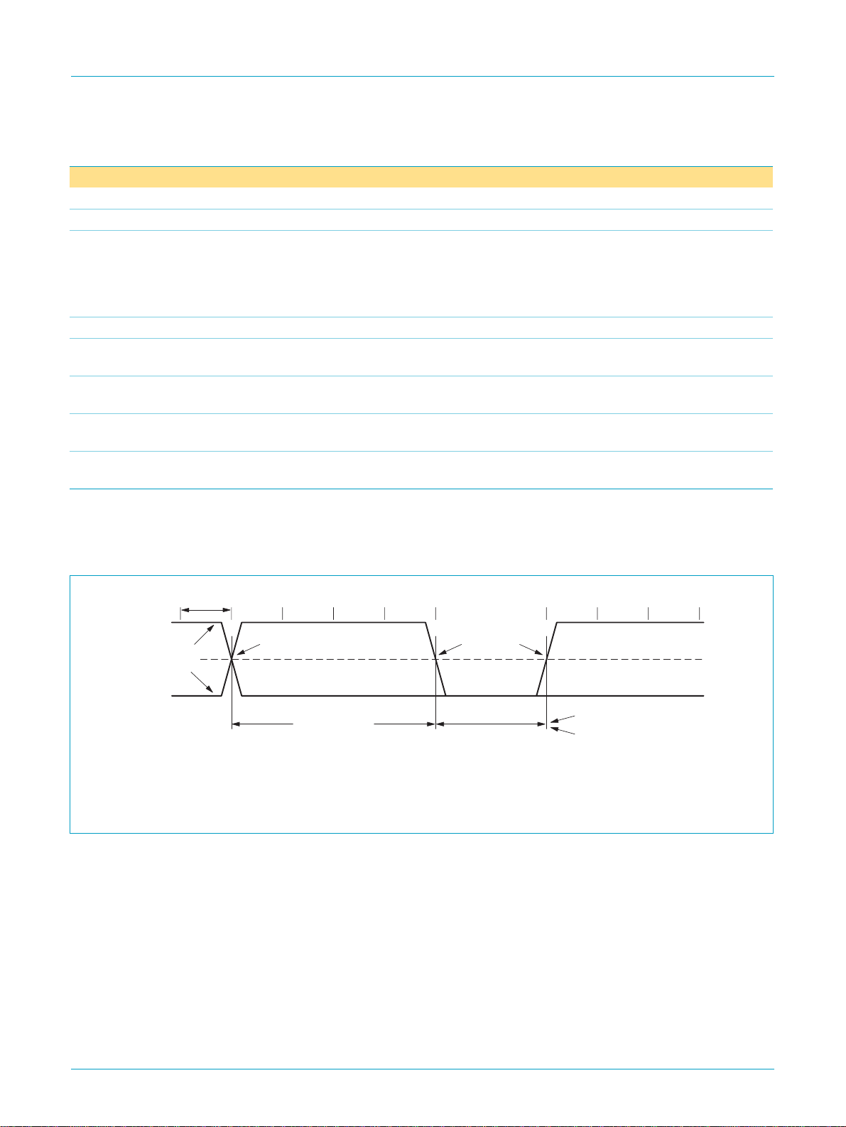
Philips Semiconductors
ISP1581
USB 2.0 HS interface device
[1]
Table 76: Dynamic characteristics: analog I/O pins (D+, D−)
VCC= 4.0 to 5.5 V; V
GND
=0V;T
=−40 to+85°C; CL= 50 pF; RPU= 1.5 kΩon D+to V
amb
Symbol Parameter Conditions Min. Typ Max Unit
Receiver timing
High-speed mode (Template 4,
- data source jitter and receiver
jitter tolerance
Universal Serial Bus Specification Rev. 2.0
eye patterns of
Template 3 and
Template 4; see
Figure 9 and
Figure 10
Full-speed mode
t
JR1
receiver data jitter tolerance to
see Figure 4
next transition
t
JR2
receiverdata jitter tolerance for
see Figure 4
paired transitions
t
FEOPR
receiver SE0 width accepted as EOP;
see Figure 3
t
FST
width of SE0 during differential
transition
rejected as EOP;
see Figure 5
…continued
)
.; unless otherwise specified.
TERM
[3]
[3]
−18.5 - +18.5 ns
[3]
−9- +9ns
[3]
82--ns
[3]
--14ns
see Table 80
[1] Test circuit: see Figure 31.
[2] Excluding the first transition from Idle state.
[3] Characterized only, not tested. Limits guaranteed by design.
T
PERIOD
+3.3 V
differential
data lines
0 V
T
is the bit duration corresponding with the USB data rate.
PERIOD
Full-speed timing symbols have a subscript prefix ‘F’, low-speed timings a prefix ‘L’.
crossover point
differential data to
SE0/EOP skew
N × T
PERIOD
+ t
DEOP
crossover point
extended
Fig 3. Source differential data-to-EOP transition skew and EOP width.
source EOP width: t
receiver EOP width: t
EOPT
EOPR
MGR776
9397 750 07648
Objective specification Rev. 02 — 23 October 2000 45 of 73
© Philips Electronics N.V. 2000. All rights reserved.
Page 46
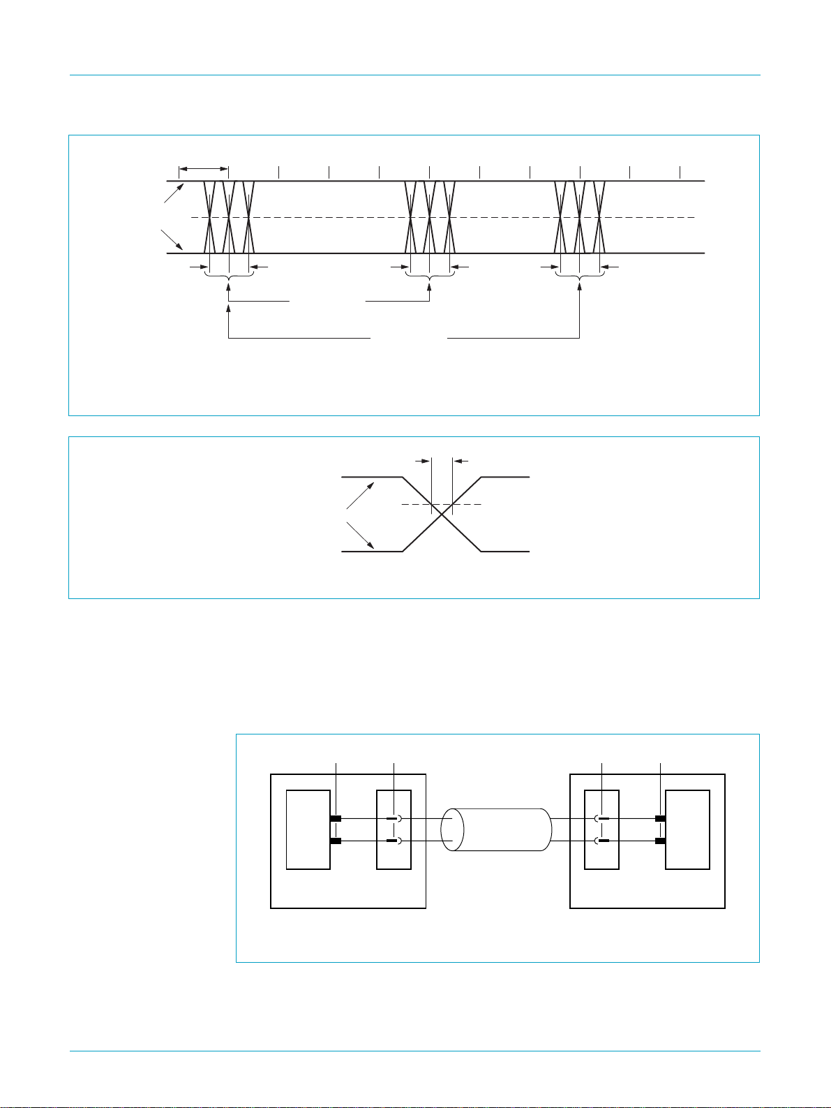
Philips Semiconductors
T
PERIOD
+3.3 V
differential
data lines
ISP1581
USB 2.0 HS interface device
0 V
T
is the bit duration corresponding with the USB data rate.
PERIOD
t
JR
N × T
Fig 4. Receiver differential data jitter.
Fig 5. Receiver SE0 width tolerance.
12.1 High-speed signals
High-speed USB signals are characterized using eyepatterns. For measuring the eye
patterns 4 test points have been defined (see Figure 6). The
Specification Rev. 2.0
Templates 1, 2, 3 and 4 are relevant.
consecutive
transitions
PERIOD
+3.3 V
differential
data lines
0 V
MGR871
+ t
JR1
N × T
paired
transitions
PERIOD
+ t
JR2
t
t
FST
JR1
V
IH(min)
MGR872
t
JR2
Universal Serial Bus
defines the eye patterns in several ‘templates’. For ISP1581
transceiver
hub circuit board
TP1 TP2
traces
connector
USB cable
A
MBL205
TP3 TP4
traces
B
connector
device circuit board
transceiver
Fig 6. Eye pattern measurement planes.
9397 750 07648
Objective specification Rev. 02 — 23 October 2000 46 of 73
© Philips Electronics N.V. 2000. All rights reserved.
Page 47

Philips Semiconductors
12.1.1 Template 1 (transmit waveform; device without captive cable)
The eye pattern in Figure 7 defines the transmit waveform requirements for a hub
(measured at TP2) or a device without a captive1 cable (measured at TP3). The
corresponding signal levels and timings are given in Table 77. Timings are given as a
percentage of the unit interval (UI), which represents the nominal bit duration T
for a 480 Mbit/s transmission rate.
ISP1581
USB 2.0 HS interface device
PERIOD
point 6
MBL206
level 1
+400 mV
point 2point 1
0
−400 mV
level 2
differential
output
voltage
(mV)
600
500
400
300
200
100
0
−100
−200
−300
−400
−500
−600
0 100relative duration
point 3 point 4
point 5
(% of unit interval)
Fig 7. Template 1 eye pattern (transmit waveform).
Table 77: Template 1 eye pattern definition
Name Differential voltage on DP, DM
(mV)
+475
−475
[1]
[2]
[1]
[2]
Level 1 +525
Level 2 −525
Relative duration
(% of unit interval)
n.a.
n.a.
Point 1 0 7.5
Point 2 0 92.5
Point 3 +300 37.5
Point 4 +300 62.5
Point 5 −300 37.5
Point 6 −300 62.5
[1] In the unit interval following a transition.
[2] In all other cases.
1. Captive cables have a vendor-specificconnectorto the peripheral (hardwired or detachable) and a USB “A” connector on the other side.
For hot plugging, the vendor-specific connector must meet the same performance requirements as a USB “B” connector.
9397 750 07648
Objective specification Rev. 02 — 23 October 2000 47 of 73
© Philips Electronics N.V. 2000. All rights reserved.
Page 48
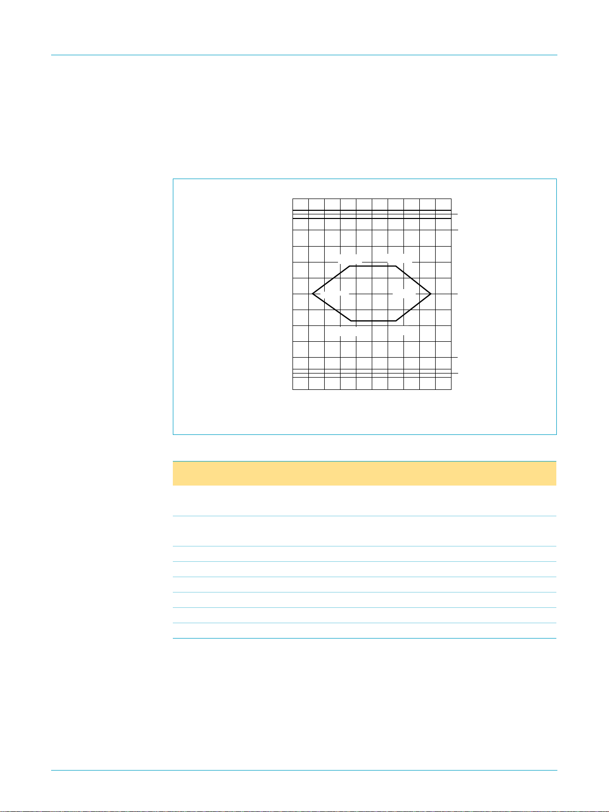
Philips Semiconductors
12.1.2 Template 2 (transmit waveform; device with captive cable)
The eye pattern in Figure 8 defines the transmit waveform requirements for a device
with a captive cable (measured at TP2). The corresponding signal levels and timings
are given in Table 78. Timings are given as a percentage of the unit interval (UI),
which represents the nominal bit duration T
PERIOD
ISP1581
USB 2.0 HS interface device
for a 480 Mbit/s transmission rate.
point 4
point 2point 1
point 6
004aaa002
level 1
+400 mV
0
−400 mV
level 2
differential
output
voltage
(mV)
600
500
400
300
200
100
0
−100
−200
−300
−400
−500
−600
0 100relative duration
point 3
point 5
(% of unit interval)
Fig 8. Template 2 eye pattern (transmit waveform).
Table 78: Template 2 eye pattern definition
Name Differential voltage on DP, DM
(mV)
+475
−475
[1]
[2]
[1]
[2]
Level 1 +525
Level 2 −525
Relative duration
(% of unit interval)
n.a.
n.a.
Point 1 0 12.5
Point 2 0 87.5
Point 3 +175 35
Point 4 +175 65
Point 5 −175 35
Point 6 −175 65
[1] In the unit interval following a transition.
[2] In all other cases.
9397 750 07648
Objective specification Rev. 02 — 23 October 2000 48 of 73
© Philips Electronics N.V. 2000. All rights reserved.
Page 49
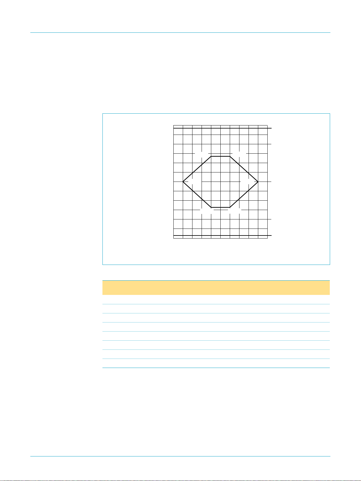
Philips Semiconductors
12.1.3 Template 3 (receive waveform; receiver sensitivity with captive cable)
The eye pattern defined in Figure 9 defines the receiver sensitivity requirements for a
device with a captive cable (signal applied at test point TP2). The corresponding
signal levels and timings are given in Table 79. Timings are given as a percentage of
the unit interval (UI), which represents the nominal bit duration T
480 Mbit/s transmission rate.
ISP1581
USB 2.0 HS interface device
for a
PERIOD
point 4
point 2
004aaa003
level 1
+400 mV
0
−400 mV
level 2
differential
input
voltage
(mV)
600
500
400
300
200
100
0
−100
−200
−300
−400
−500
−600
0 100relative duration
point 3
point 1
point 5
(% of unit interval)
point 6
Fig 9. Template 3 eye pattern (receive waveform).
Table 79: Template 3 eye pattern definition
Name Differential voltage on DP, DM
(mV)
Relative duration
(% of unit interval)
Level 1 +575 n.a.
Level 2 −575 n.a.
Point 1 0 10
Point 2 0 90
Point 3 +275 40
Point 4 +275 60
Point 5 −275 40
Point 6 −275 60
9397 750 07648
Objective specification Rev. 02 — 23 October 2000 49 of 73
© Philips Electronics N.V. 2000. All rights reserved.
Page 50
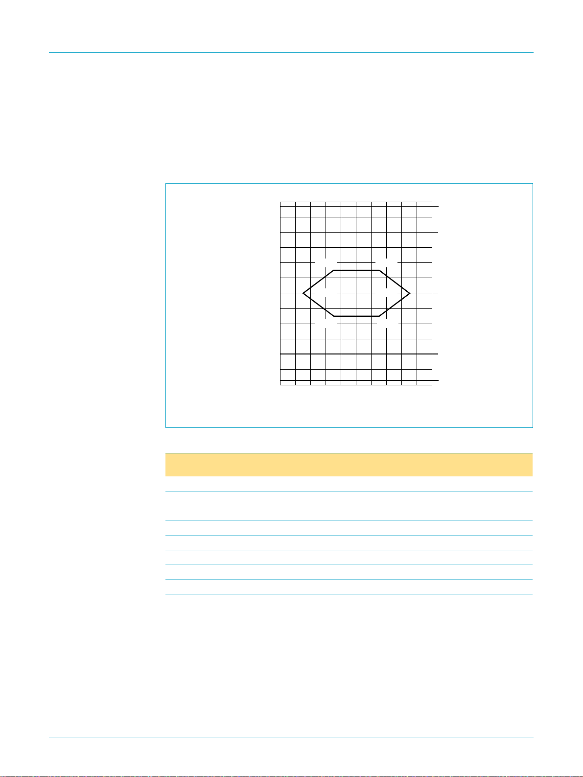
Philips Semiconductors
12.1.4 Template 4 (receive waveform; receiver sensitivity without captive cable)
The eye pattern defined in Figure 10 defines the receiver sensitivity requirements for
a hub (signal applied at test point TP2) or a device without a captive cable (signal
applied at test point TP3). The corresponding signal levels and timings are given in
Table 80. Timings are given as a percentage of the unit interval (UI), which represents
the nominal bit duration T
for a 480 Mbit/s transmission rate.
PERIOD
ISP1581
USB 2.0 HS interface device
point 2
MBL207
level 1
+400 mV
0
−400 mV
level 2
differential
input
voltage
(mV)
600
500
400
300
200
100
0
−100
−200
−300
−400
−500
−600
0 100relative duration
point 3 point 4
point 1
point 5 point 6
(% of unit interval)
Fig 10. Template 4 eye pattern (receive waveform).
Table 80: Template 4 eye pattern definition
Name Differential voltage on DP, DM
(mV)
Relative duration
(% of unit interval)
Level 1 +575 n.a.
Level 2 −575 n.a.
Point 1 0 15
Point 2 0 85
Point 3 +150 35
Point 4 +150 65
Point 5 −150 35
Point 6 −150 65
9397 750 07648
Objective specification Rev. 02 — 23 October 2000 50 of 73
© Philips Electronics N.V. 2000. All rights reserved.
Page 51

Philips Semiconductors
12.2 Timing symbols
Table 81: Legend for timing characteristics
Symbol Description
Time symbols
t time
T cycle time (periodic signal)
Signal names
A address;
C clock;
D data input;
E chip enable
G output enable
I instruction (program memory content);
L address latch enable (ALE)
P program store enable (
Q data output
R read signal (
S chip select
W write signal (
U undefined
Y output (general)
Logic levels
H logic HIGH
L logic LOW
P stop, not active (OFF)
S start, active (ON)
V valid logic level
X invalid logic level
Z high-impedance (floating, three-state)
ISP1581
USB 2.0 HS interface device
DMA acknowledge (DACK)
command
data
input (general)
PSEN, active LOW);
propagation delay
RD, active LOW);
read (action);
DMA request (DREQ)
WR, active LOW);
write (action);
pulse width
9397 750 07648
Objective specification Rev. 02 — 23 October 2000 51 of 73
© Philips Electronics N.V. 2000. All rights reserved.
Page 52
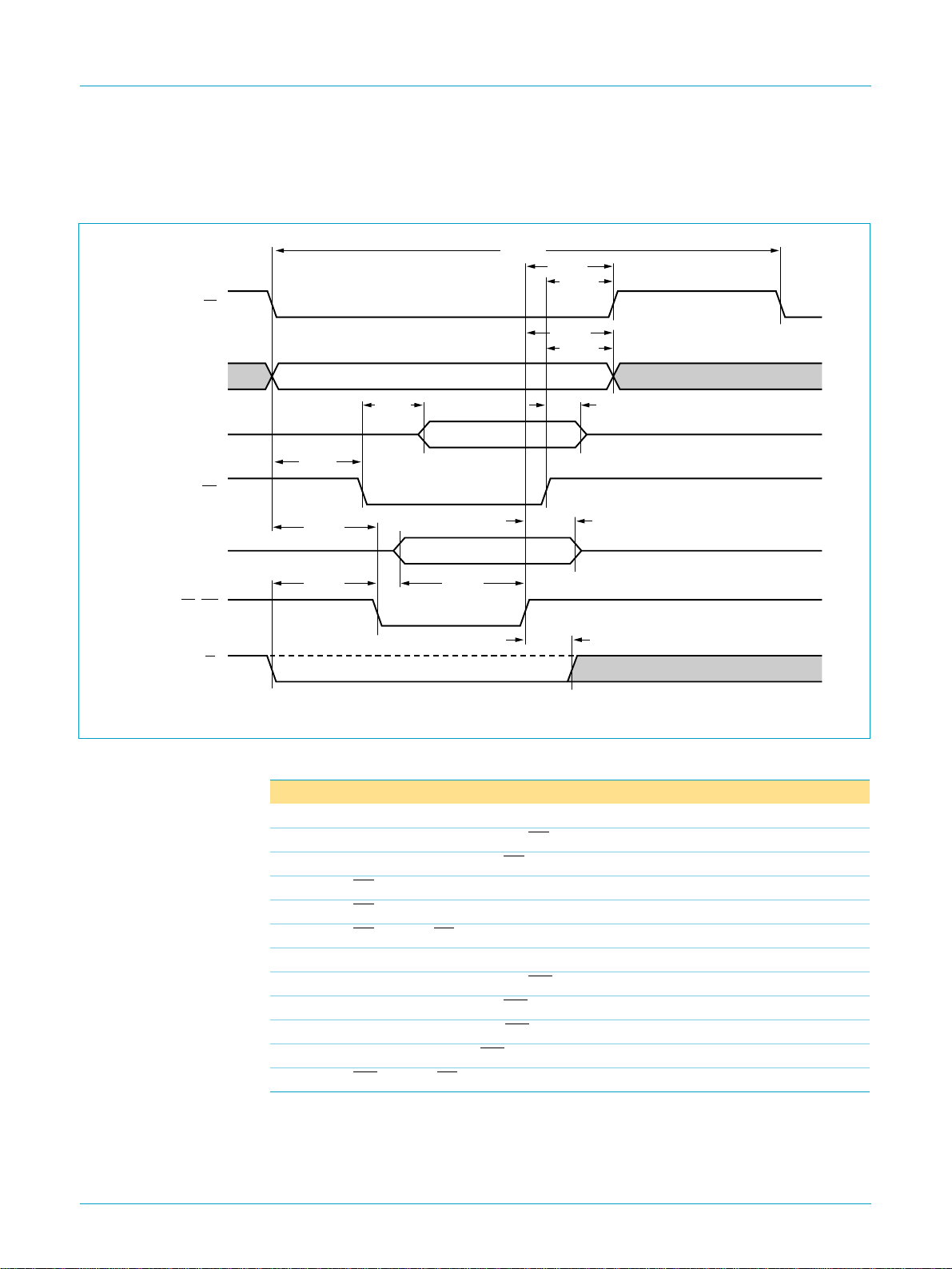
Philips Semiconductors
12.3 Parallel I/O timing
12.3.1 Generic Processor mode (BUS_CONF = 1)
CS
]
AD[7:0
(read) DATA[15:0
(write) DATA[15:0
]
RD
]
t
AVRL
t
AVWL
t
RLDV
T
cy(RW)
t
WHDZ
t
WHSH
t
t
WHAX
t
RHSH
RHAX
t
RHDZ
ISP1581
USB 2.0 HS interface device
DS/WR
(I2)
R/W
(I1)
t
I1VI2L
read
write
t
DVWH
Fig 11. Parallel I/O timing: separate address and data buses.
Table 82: Parallel I/O timing parameters: separate address and data buses
Symbol Parameter Min Max Unit
Reading
t
AVRL
t
RHAX
t
RLDV
t
RHDZ
t
RHSH
address set-up time before RD LOW 0 - ns
address hold time after RD HIGH 0 - ns
RD LOW to data valid delay - 35 ns
RD HIGH to data outputs three-state delay 0 20 ns
RD HIGH to CS HIGH delay 0 - ns
Writing
t
AVWL
t
WHAX
t
DVWH
t
WHDZ
t
WHSH
address set-up time before WR LOW 0 - ns
address hold time after WR HIGH 0 - ns
data set-up time before WR HIGH 25 - ns
data hold time after WR HIGH 0 - ns
WR HIGH to CS HIGH delay 0 - ns
t
I2HI1X
MGT497
9397 750 07648
© Philips Electronics N.V. 2000. All rights reserved.
Objective specification Rev. 02 — 23 October 2000 52 of 73
Page 53
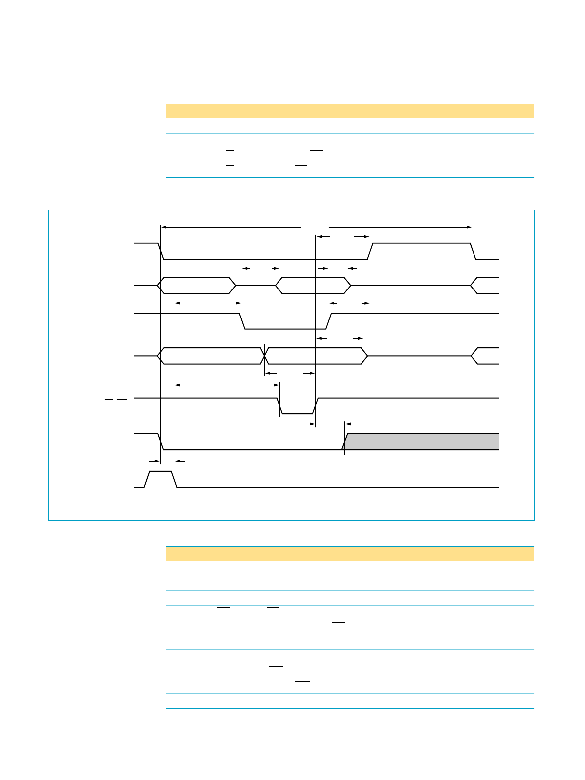
Philips Semiconductors
ISP1581
USB 2.0 HS interface device
CS
(read) AD[7:0
RD
(write) AD[7:0
DS/WR
(I2)
R/W
(I1)
ALE
Table 82: Parallel I/O timing parameters: separate address and data buses
Symbol Parameter Min Max Unit
General
T
cy(RW)
t
I1VI2L
t
I2HI1X
read/write cycle time 60 - ns
R/W set-up time before DS LOW 5 - ns
R/W hold time after DS HIGH 5 - ns
12.3.2 Split Bus mode (BUS_CONF = 0)
T
t
RLDV
]
]
address
t
LLRL
address
t
AVLL
t
I1VLL
t
LLWL
t
LLI2L
t
DVWH
data
data
cy(RW)
t
t
t
WHDZ
I2HI1X
WHSH
t
RHSH
t
RHDZ
…continued
MGT498
Fig 12. Parallel interface timing: multiplexed address/data bus.
Table 83: Parallel I/O timing parameters: multiplexed address/data bus
Symbol Parameter Min Max Unit
Reading
t
RLDV
t
RHDZ
t
RHSH
t
LLRL
RD LOW to data valid delay - 35 ns
RD HIGH to data outputs three-state delay 0 20 ns
RD HIGH to CS HIGH delay 0 - ns
ALE LOW set-up time before RD LOW 0 - ns
Writing
t
DVWH
t
LLWL
t
WHDZ
t
WHSH
9397 750 07648
Objective specification Rev. 02 — 23 October 2000 53 of 73
data set-up time before WR HIGH 25 - ns
ALE LOW to WR LOW delay 5 - ns
data hold time after WR HIGH 0 - ns
WR HIGH to CS HIGH delay 0 - ns
© Philips Electronics N.V. 2000. All rights reserved.
Page 54
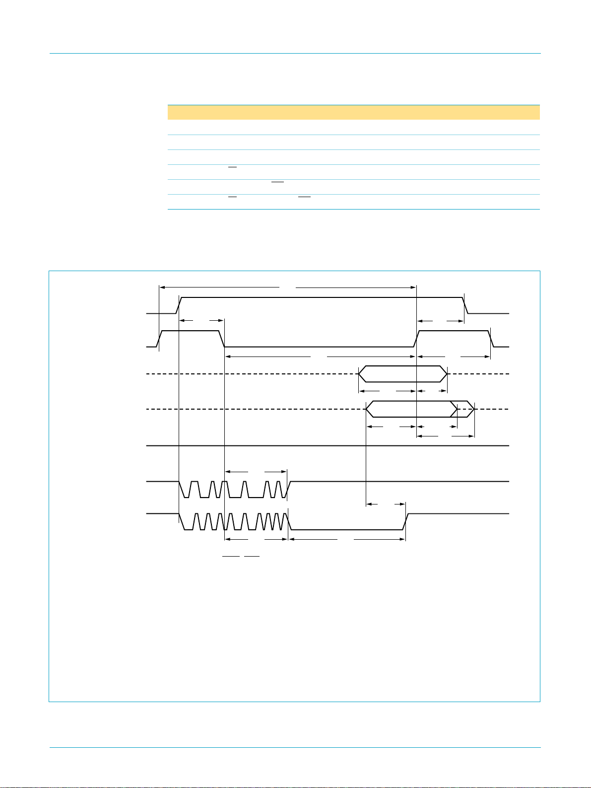
Philips Semiconductors
ISP1581
USB 2.0 HS interface device
device
address
valid
DIOR, DIOW
(write) DATA[7:0
(read) DATA[7:0
IORDY
Table 83: Parallel I/O timing parameters: multiplexed address/data bus
Symbol Parameter Min Max Unit
General
T
cy(RW)
t
AVLL
t
I1VLL
t
LLI2L
t
I2HI1X
12.4 DMA timing
12.4.1 PIO mode
(1)
t
su1
(4)
(2)
]
(2)
]
HIGH
(3a)
…continued
read/write cycle time 60 - ns
address set-up time before ALE LOW 3 - ns
R/W set-up time before ALE LOW 3 - ns
ALE LOW to DS LOW delay 5 - ns
R/W hold time after DS HIGH 5 - ns
T
cy1
t
h1
t
w1
t
su2
t
su3
t
w2
t
h2
t
h3
(min)
t
d2
t
su4
(3b)
IORDY
t
su5
(3c)
IORDY
t
su4
t
w3
MGT499
(1) The device address consists of signals CS1, CS0, DA2, DA1 and DA0.
(2) The data bus width depends on the PIO access command used. Task File register access uses 8 bits (DATA[7:0]), except
for Task File register 1F0 which uses 16 bits (DATA[15:0]). DMA commands 04H and 05H also use a 16-bit data bus.
(3) The device can negate IORDY to extend the PIO cycle with wait states. The host determines whether or not to extend the
current cycle after t
following the assertion of DIOR or DIOW. The following three cases are distinguished:
su4
a) Device keeps IORDY released (high-impedance): no wait state is generated.
b) Device negates IORDY during t
c) Device negates IORDY during t
, but re-asserts IORDY before t
su4
and keeps IORDY negated for at least 5 ns after t
su4
expires: no wait state is generated.
su4
expires: a wait state is
su4
generated. The cycle is completed as soon as IORDY is re-asserted. For extended read cycles (DIOR asserted), the
read data on lines DATAn must be valid at td1 before IORDY is asserted.
(4) DIOR and DIOW have a programmable polarity: shown here as active LOW signals.
Fig 13. PIO mode timing.
9397 750 07648
Objective specification Rev. 02 — 23 October 2000 54 of 73
© Philips Electronics N.V. 2000. All rights reserved.
Page 55

Philips Semiconductors
ISP1581
USB 2.0 HS interface device
Table 84: PIO mode timing parameters
Symbol Parameter Mode 0 Mode 1 Mode 2 Mode 3 Mode 4 Unit
T
cy1(min)
t
su1(min)
t
w1(min)
t
w2(min)
t
su2(min)
t
h2(min)
t
su3(min)
t
h3(min.)
t
d2(max)
t
h1(min)
t
su4(min)
t
su5(min)
t
w3(max)
read/write cycle time (minimum)
address to DIOR/DIOW on set-up time
(minimum)
DIOR/DIOW pulse width (minimum)
DIOR/DIOW recovery time (minimum)
data set-up time before DIOW off
(minimum)
data hold time after DIOW off (minimum) 30 20 15 10 10 ns
data set-up time before DIOR on
(minimum)
data hold time after DIOR off (minimum) 55555ns
data to three-state delay after DIOR off
(minimum)
address hold time after DIOR/DIOW off
(minimum)
IORDY after DIOR/DIOW on set-up time
(minimum)
read data to IORDY HIGH set-up time
(minimum)
IORDY LOW pulse width (maximum) 1250 1250 1250 1250 1250 ns
[1]
600 383 240 180 120 ns
70 50 30 30 25 ns
[1]
165 125 100 80 70 ns
[1]
---7025ns
60 45 30 30 20 ns
50 35 20 20 20 ns
[2]
30 30 30 30 30 ns
20 15 10 10 10 ns
[3]
35 35 35 35 35 ns
[3]
00000ns
[1] T
[2] td2 specifies the time after DIOR is negated, when the data bus is no longer driven by the device (three-state).
[3] If IORDY is LOW at t
is the total cycle time, consisting of the command active time tw1and is the command recovery (= inactive) time tw2:T
cy1
The minimum timing requirements for T
host implementation must lengthen tw1 and/or tw2 to ensure that T
DEVICE data. A device implementation shall support any legal host implementation.
, the host waits until IORDY is made HIGH before the PIO cycle is completed. In that case, t
reading (t
su3
su4
does not apply). When IORDY is HIGH at t
, tw1and tw2 must all be met. Since T
cy1
su4
, t
is equal to or greater than the value reported in the IDENTIFY
cy1
must be met for reading (t
su3
is greater than the sum of t
cy1(min)
does not apply).
su5
cy1=tw1+tw2
and t
w1(min)
must be met for
su5
w2(min)
.
, a
9397 750 07648
Objective specification Rev. 02 — 23 October 2000 55 of 73
© Philips Electronics N.V. 2000. All rights reserved.
Page 56
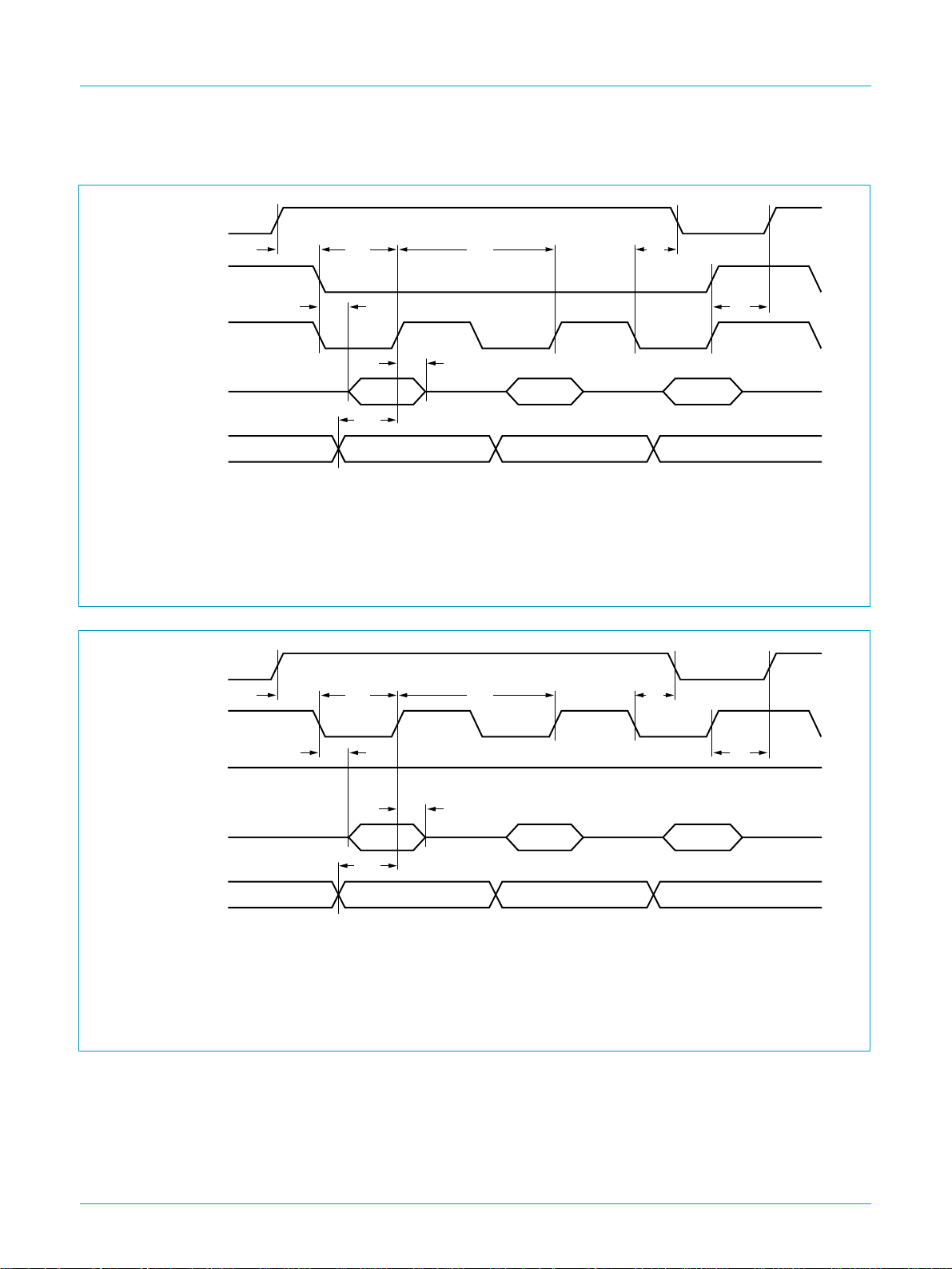
Philips Semiconductors
12.4.2 GDMA slave mode
(2)
DREQ
(1)
DACK
ISP1581
USB 2.0 HS interface device
t
su1
t
w1
T
cy1
t
h1
t
d2
DIOR/DIOW
(read) DATA[15:0
(write) DATA[15:0
(1)
t
h2
]
t
su2
]
DREQ is continuously asserted until the last transfer is done or the FIFO is full.
Data strobes: DIOR (read), DIOW (write).
(1) Programmable polarity: shown as active LOW.
(2) Programmable polarity: shown as active HIGH.
Fig 14. GDMA slave mode timing (BURST = 00H, MODE = 00H).
(2)
DREQ
t
w1
t
d2
t
h2
t
su2
T
cy1
DACK
DIOR/DIOW
(read) DATA[15:0
(write) DATA[15:0
t
su1
(1)
(1)
]
]
HIGH
t
d1
MGT500
t
h1
t
d1
MGT501
DREQ is continuously asserted until the last transfer is done or the FIFO is full.
Data strobe: DACK (read/write).
(1) Programmable polarity: shown as active LOW.
(2) Programmable polarity: shown as active HIGH.
Fig 15. GDMA slave mode timing (BURST = 00H, MODE = 02H).
9397 750 07648
Objective specification Rev. 02 — 23 October 2000 56 of 73
© Philips Electronics N.V. 2000. All rights reserved.
Page 57
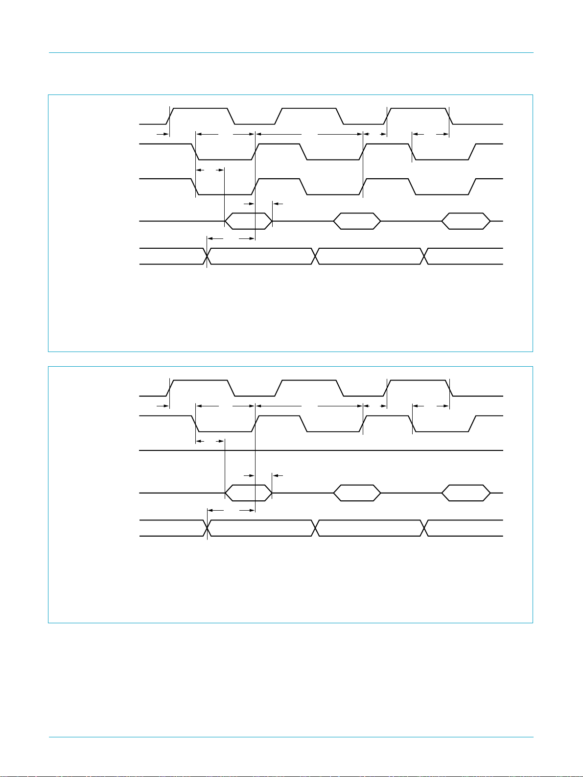
Philips Semiconductors
(2)
DREQ
t
su1
(1)
DACK
DIOR/DIOW
(read) DATA[15:0
(write) DATA[15:0
(1)
]
]
DREQ is asserted for every transfer.
Data strobes: DIOR (read), DIOW (write).
(1) Programmable polarity: shown as active LOW.
(2) Programmable polarity: shown as active HIGH.
Fig 16. GDMA slave mode timing (BURST = 01H, MODE = 00H).
t
w1
t
d2
t
h2
t
su2
ISP1581
USB 2.0 HS interface device
T
cy1
t
d1
t
h1
MGT502
(2)
DREQ
DACK
DIOR/DIOW
(read) DATA[15:0
(write) DATA[15:0
t
su1
(1)
(1)
]
]
HIGH
t
w1
t
d2
t
h2
t
su2
T
cy1
DREQ is asserted for every transfer.
Data strobe: DACK (read/write).
(1) Programmable polarity: shown as active LOW.
(2) Programmable polarity: shown as active HIGH.
Fig 17. GDMA slave mode timing (BURST = 01H, MODE = 02H).
t
d1
t
h1
MGT503
9397 750 07648
© Philips Electronics N.V. 2000. All rights reserved.
Objective specification Rev. 02 — 23 October 2000 57 of 73
Page 58
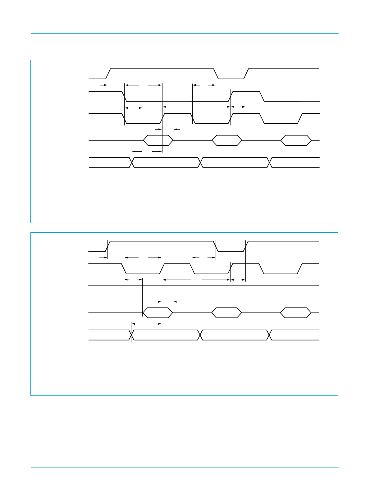
Philips Semiconductors
(2)
DREQ
t
w1
t
d2
t
h2
t
su2
DACK
DIOR/DIOW
(read) DATA[15:0
(write) DATA[15:0
t
su1
(1)
(1)
]
]
DREQ is asserted once per N transfers (N is determined by the BURST value). Example shown here: N = 2.
Data strobes: DIOR (read), DIOW (write).
(1) Programmable polarity: shown as active LOW.
(2) Programmable polarity: shown as active HIGH.
Fig 18. GDMA slave mode timing (BURST > 01H, MODE = 00H).
t
h1
T
cy1
t
d1
ISP1581
USB 2.0 HS interface device
MGT504
(2)
DREQ
t
h1
T
cy1
t
d1
DACK
DIOR/DIOW
(read) DATA[15:0
(write) DATA[15:0
t
su1
(1)
(1)
HIGH
]
]
t
w1
t
d2
t
h2
t
su2
DREQ is asserted once per N transfers (N is determined by the BURST value). Example shown here: N = 2.
Data strobe: DACK (read/write).
(1) Programmable polarity: shown as active LOW.
(2) Programmable polarity: shown as active HIGH.
Fig 19. GDMA slave mode timing (BURST > 01H, MODE = 02H).
MGT505
9397 750 07648
© Philips Electronics N.V. 2000. All rights reserved.
Objective specification Rev. 02 — 23 October 2000 58 of 73
Page 59
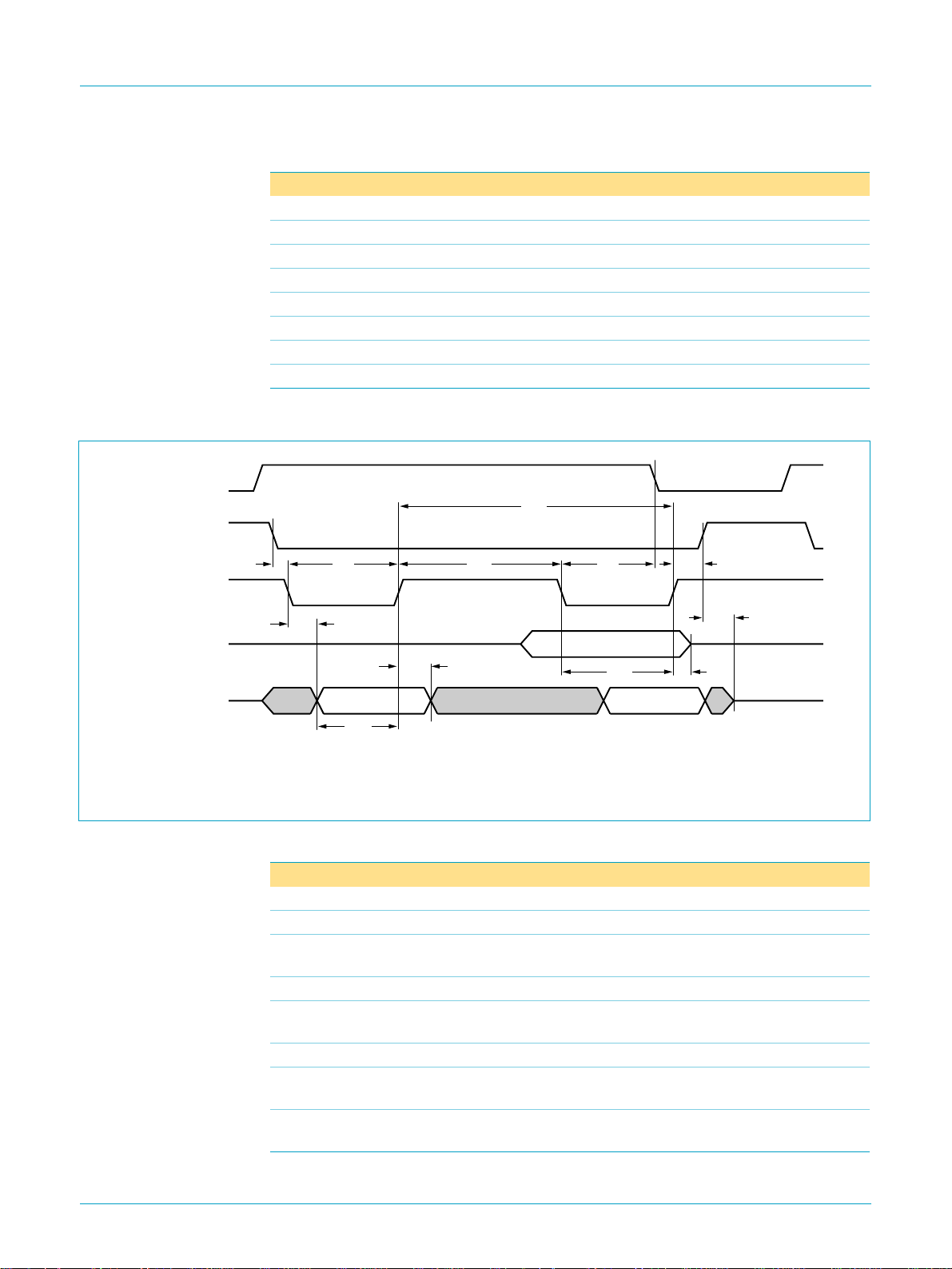
Philips Semiconductors
Table 85: GMDA slave mode timing parameters
Symbol Parameter Min Max Unit
T
cy1
t
su1
t
d1
t
h1
t
w1
t
d2
t
h2
t
su2
12.4.3 MDMA mode
(2)
DREQ
(1)
DACK
t
su1
DIOR/DIOW
(write) DATA[15:0
(read) DATA[15:0
(1)
]
]
ISP1581
USB 2.0 HS interface device
read/write cycle time 66.67 - ns
DREQ set-up time before first DACK on 0 - ns
DREQ on delay after last strobe off 33.33 - ns
DREQ hold time after last strobe on 0 33.33 ns
DIOR/DIOW pulse width 33.33 - ns
read data valid delay after strobe on - 10 ns
read data hold time after strobe off 5 - ns
write data set-up time before strobe off 10 - ns
T
cy1
t
w1
t
d1
t
h3
t
su2
t
w2
t
d2
t
su2
t
h1
t
d3
t
h2
MGT506
(1) Programmable polarity: shown as active LOW.
(2) Programmable polarity: shown as active HIGH.
Fig 20. MDMA master mode timing.
Table 86: MDMA mode timing parameters
Symbol Parameter Mode 0 Mode 1 Mode 2 Unit
T
cy1(min)
t
w1(min)
t
d1(max)
read/write cycle time (minimum)
DIOR/DIOW pulse width (minimum)
data valid delay after DIOR on
[1]
480 150 120 ns
[1]
215 80 70 ns
150 60 50 ns
(maximum)
t
h3(min)
t
su2(min)
data hold time after DIOR off (minimum) 555ns
data set-up time before DIOR/DIOW off
100 30 20 ns
(minimum)
t
h2(min)
t
su1(min)
data hold time after DIOW off (minimum) 20 15 10 ns
DACKset-uptime before DIOR/DIOW on
000ns
(minimum)
t
h1(min)
DACK hold time after DIOR/DIOW off
2055ns
(minimum)
9397 750 07648
Objective specification Rev. 02 — 23 October 2000 59 of 73
© Philips Electronics N.V. 2000. All rights reserved.
Page 60
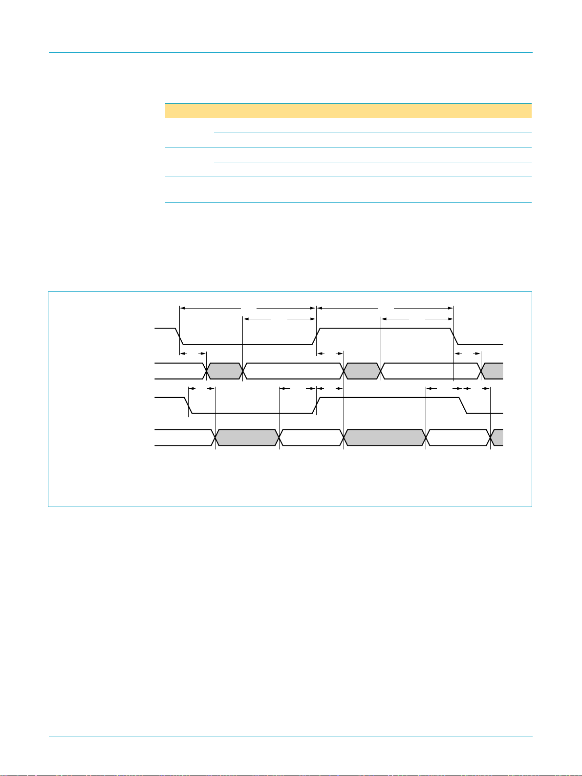
Philips Semiconductors
ISP1581
USB 2.0 HS interface device
DIOR
DATA[15:0]
IORDY
Table 86: MDMA mode timing parameters
Symbol Parameter Mode 0 Mode 1 Mode 2 Unit
t
w2(min)
t
d2(max)
t
d3(max)
[1] T
(= inactive) time tw2: T
be met. Since T
lengthen tw1 and/or tw2 to ensure that T
IDENTIFY DEVICE data. A device implementation shall support any legal host implementation.
12.4.4 UDMA mode
(1)
(sender)
(1)
(sender)
(1)
(receiver)
…continued
DIOR recovery time (minimum)
DIOW recovery time (minimum)
[1]
[1]
50 50 25 ns
215 50 25 ns
DIOR on to DREQ off delay (maximum) 120 40 35 ns
DIOW on to DREQ off delay (maximum) 40 40 35 ns
DACK off to data lines three-state delay
20 25 25 ns
(maximum)
is the total cycle time, consisting of the command active time tw1and is the command recovery
cy1
t
cy1=tw1+tw2
is greater than the sum of t
cy1(min)
T
cy1
t
su1
h1
t
h2
. The minimum timing requirements for T
and t
t
su2
w1(min)
is equal to or greater than the value reported in the
cy1
t
h1
t
h2
w2(min)
T
cy1
, tw1and tw2 must all
cy1
, a host implementation must
t
su1
t
h1
t
su2
t
h2
(1)
DATA[15:0]
(receiver)
(1) DATA[15:0] and strobe signals at the receiver require some time to stabilize due to the settling time and propagation delay
of the cable.
Fig 21. UDMA timing: sustained synchronous burst.
MGT507
9397 750 07648
© Philips Electronics N.V. 2000. All rights reserved.
Objective specification Rev. 02 — 23 October 2000 60 of 73
Page 61
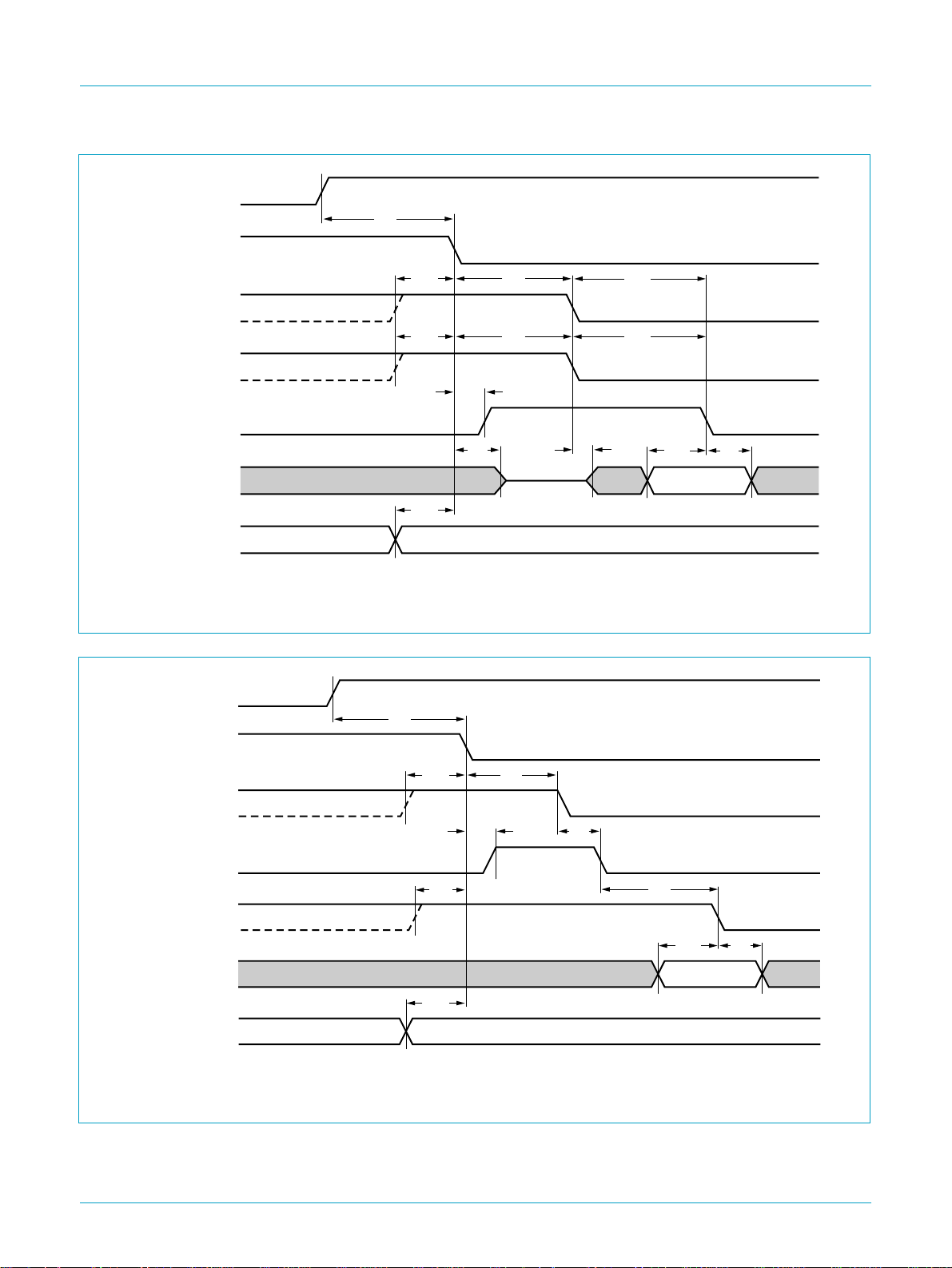
Philips Semiconductors
DREQ (drive)
(1)
(host)
DACK
ISP1581
USB 2.0 HS interface device
t
d1
DIOW (host)
DIOR (host)
IORDY (drive)
DATA[15:0] (drive)
DA[2:0] and CS[1:0
t
su3
t
su3
t
su3
]
t
d11
t
t
d6
t
d6
d4
(1) Programmable polarity: shown as active LOW.
Fig 22. UDMA timing: drive initiating a burst for a read command.
DREQ (drive)
t
d1
(1)
(host)
DACK
DIOW (host)
IORDY (drive)
t
su3
t
d11
t
d6
t
d13
t
d13
t
d5
t
d2
t
su1
t
h1
MGT508
t
d1
t
su1
t
h1
MGT509
DIOR (host)
DATA[15:0] (host)
DA[2:0] and CS[1:0
t
su3
t
su3
]
(1) Programmable polarity: shown as active LOW.
Fig 23. UDMA timing: drive initiating a burst for a write command.
9397 750 07648
Objective specification Rev. 02 — 23 October 2000 61 of 73
© Philips Electronics N.V. 2000. All rights reserved.
Page 62
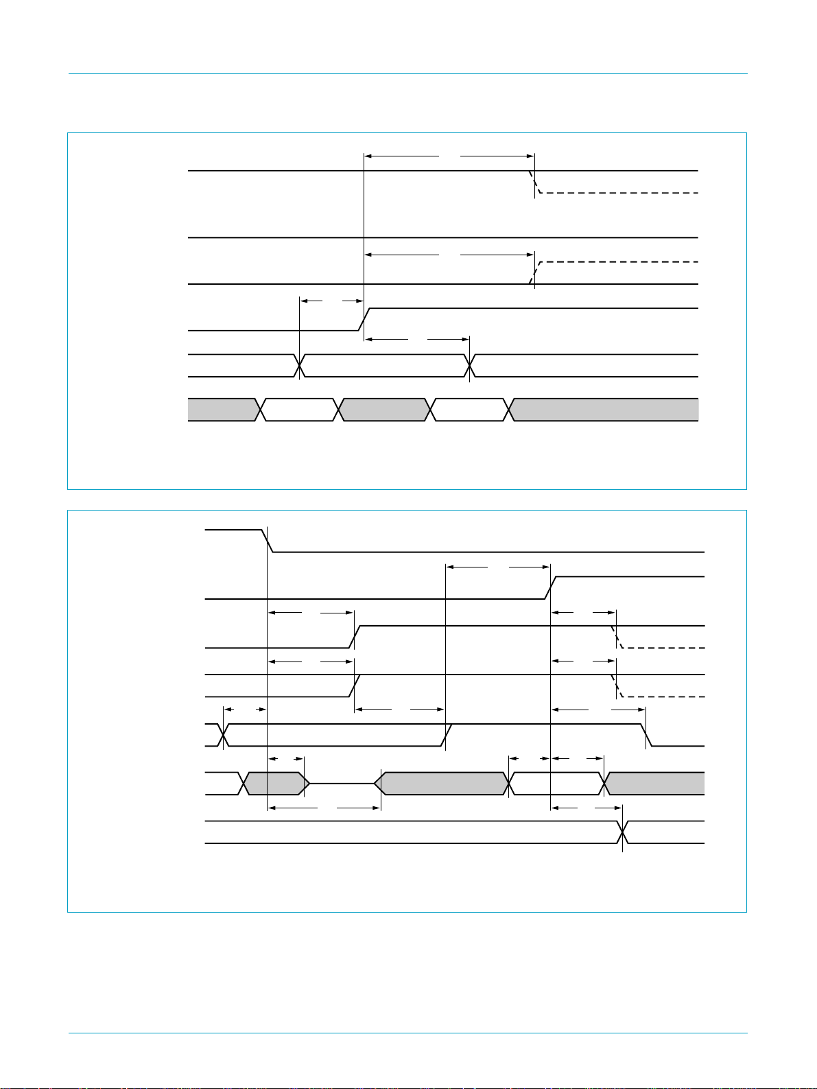
Philips Semiconductors
DREQ (drive)
(1)
(host)
DACK
DIOW (host)
IORDY
DIOR
LOW
ISP1581
USB 2.0 HS interface device
t
d7
t
d7
t
d8
t
d9
DATA[15:0
]
(1) Programmable polarity: shown as active LOW.
Fig 24. UDMA timing: receiver pausing a burst.
DREQ (drive)
(1)
DACK
(host)
t
d2
DIOW (host)
t
d2
DIOR (host)
t
d12
IORDY (drive)
t
d4
DATA[15:0] (drive)
t
d5
DA[2:0] and CS[1:0
]
MGT510
t
d3
t
h3
t
h3
t
d2
t
su1
t
CRC
t
d10
h1
t
h3
MGT511
(1) Programmable polarity: shown as active LOW.
Fig 25. UDMA timing: drive terminating a burst during a read command.
9397 750 07648
Objective specification Rev. 02 — 23 October 2000 62 of 73
© Philips Electronics N.V. 2000. All rights reserved.
Page 63
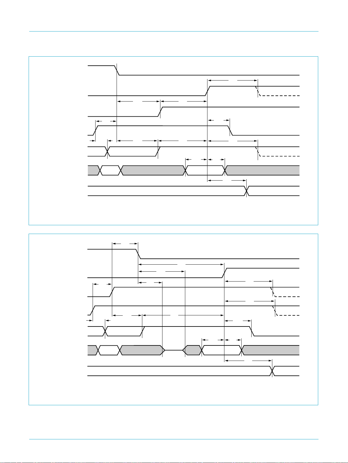
Philips Semiconductors
DREQ (drive)
(1)
DACK
(host)
DIOW (host)
t
IORDY (drive)
t
d9
DIOR (host)
ISP1581
USB 2.0 HS interface device
t
h3
t
d2
d7
t
d2
t
d3
t
d10
t
d3
t
su1
t
h3
t
h1
DATA[15:0] (host)
DA[2:0] and CS[1:0
]
CRC
(1) Programmable polarity: shown as active LOW.
Fig 26. UDMA timing: drive terminating a burst during a write command.
t
d2
DREQ (drive)
t
d3
t
d3
(1)
(host)
DACK
DIOW (host)
DIOR (host)
IORDY (drive)
DATA[15:0] (drive)
DA[2:0] and CS[1:0
t
d5
t
t
d7
t
t
d9
]
d2
d4
t
su1
CRC
t
h3
MGT512
t
h3
t
h3
t
d10
t
h1
t
h3
MGT513
(1) Programmable polarity: shown as active LOW.
Fig 27. UDMA timing: host terminating a burst during a read command.
9397 750 07648
Objective specification Rev. 02 — 23 October 2000 63 of 73
© Philips Electronics N.V. 2000. All rights reserved.
Page 64
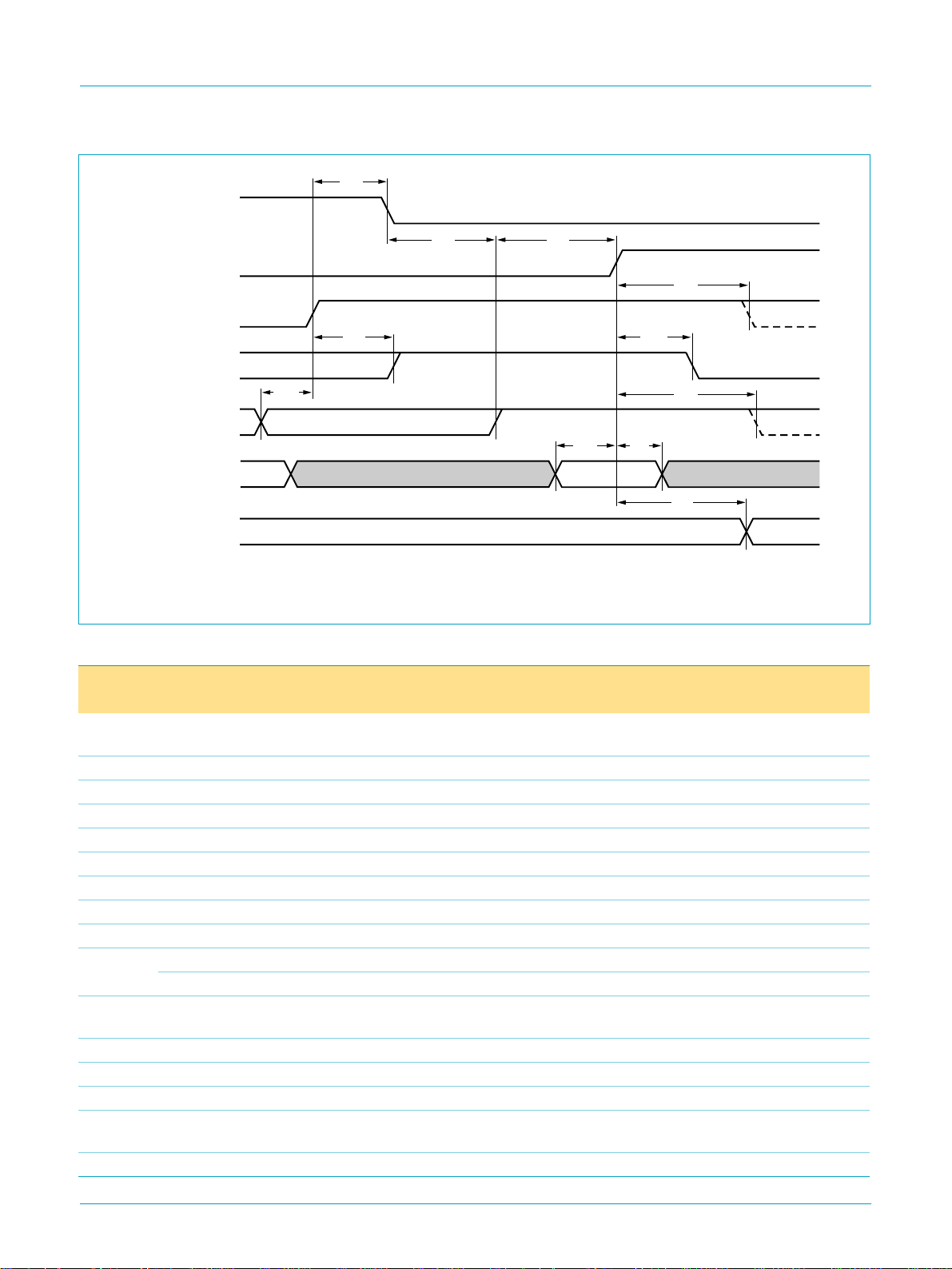
Philips Semiconductors
DREQ (drive)
ISP1581
USB 2.0 HS interface device
t
d2
(1)
DACK
(host)
DIOW (host)
IORDY (drive)
DIOR (host)
DATA[15:0] (host)
DA[2:0] and CS[1:0
t
d2
t
d2
t
d12
]
t
d3
t
h3
t
d10
t
h3
t
su1
CRC
t
h1
t
h3
MGT514
(1) Programmable polarity: shown as active LOW.
Fig 28. UDMA timing: host terminating a burst during a write command.
Table 87: UDMA mode timing parameters
Symbol Parameter Mode 0 Mode 1 Mode 2 Unit
Min Max Min Max Min Max
T
cy1
read/write cycle time (from strobe edge
114 - 75 - 55 - ns
to strobe edge)
t
t
t
t
t
t
t
t
t
su2
h2
su1
h1
d1
d2
d3
d4
d5
data set-up time at receiver 15 - 10 - 7 - ns
data hold time at receiver 5-5-5-ns
data set-up time at sender 70 - 48 - 34 - ns
data hold time at sender 6-6-6-ns
unlimited interlock time
limited interlock time
limited interlock time with minimum
[1]
[1]
[1]
0-0-0-ns
0 150 0 150 0 150 ns
20 - 20 - 20 - ns
data line drivers switch-off delay - 10 - 10 - 10 ns
data line drivers switch-on delay (host) 20 - 20 - 20 - ns
data line drivers switch-on delay (drive) 0-0-0-ns
t
su3
control signal set-up time before DACK
20 - 20 - 20 - ns
on
t
h3
t
d6
t
d7
t
d8
control signal hold time after DACK off 20 - 20 - 20 - ns
DACKon to control signal transition delay 20 70 20 70 20 70 ns
ready to paused delay 160 - 125 - 100 - ns
strobe to ready delay to ensure a
-50-30-20ns
synchronous pause
t
d9
ready to final strobe edge delay - 75 - 60 - 50 ns
9397 750 07648
© Philips Electronics N.V. 2000. All rights reserved.
Objective specification Rev. 02 — 23 October 2000 64 of 73
Page 65
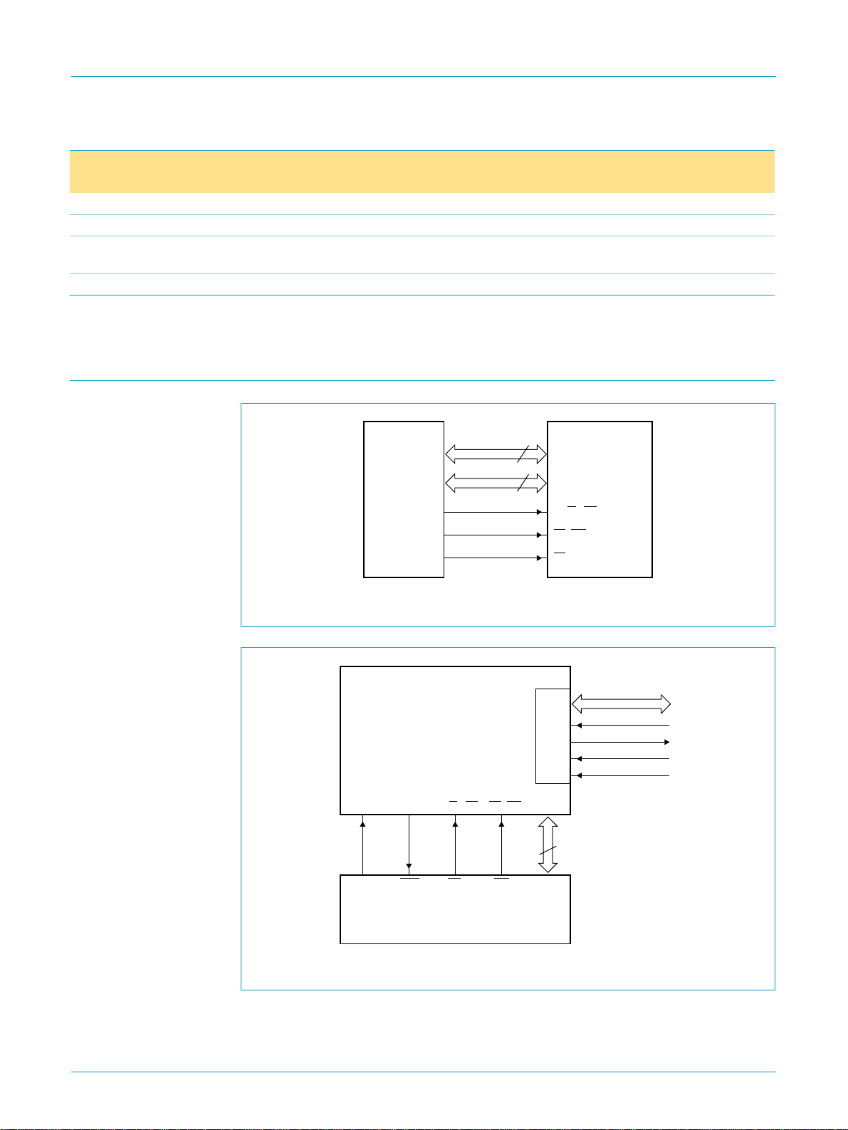
Philips Semiconductors
ISP1581
USB 2.0 HS interface device
Table 87: UDMA mode timing parameters
…continued
Symbol Parameter Mode 0 Mode 1 Mode 2 Unit
Min Max Min Max Min Max
t
t
t
d10
d11
d12
DACK off to IORDY high-Z delay - 20 - 20 - 20 ns
DACK on to IORDY HIGH delay 0-0-0-ns
final strobe edge to DREQ off or DIOW
50 - 50 - 50 - ns
on delay
t
d13
[1] Interlock time is the time allowed between an action by one agent and the following action by the other agent. An agent can be a sender
or a receiver. Interlocking actions require a response signal from the other agent before processing can continue.
first strobe delay after control signal on 0 230 0 200 0 170 ns
13. Application information
ISP1581
AD7 to AD0
DATA15 to DATA0
(R/W)/RD
DS/WR
CS
CPU
address 8
data
read strobe
write strobe
chip select
16
MGT515
Fig 29. Typical interface connections for Generic Processor mode.
DATA[15:0
DREQ
DACK
DIOW
DIOR
address/data
8
ALE
INTALE/A0
address
latch
enable
interrupt
MICROCONTROLLER
ISP1581
(R/W)/RD DS/WR
RDINTn
8051
read
strobe
WR
write
strobe
DMA
AD7 to
AD0
P0.7/AD7
to
P0.0/AD0
MGT516
Fig 30. Typical interface connections for Split Bus mode.
]
9397 750 07648
© Philips Electronics N.V. 2000. All rights reserved.
Objective specification Rev. 02 — 23 October 2000 65 of 73
Page 66
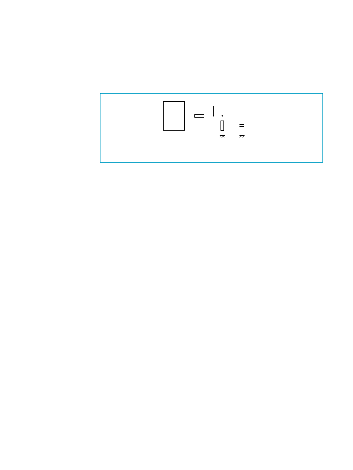
Philips Semiconductors
14. Test information
The dynamic characteristics of the analog I/O ports (D+, D−) as listed in Table 76,
were determined using the circuit shown in Figure 31.
Fig 31. Load impedance for D+ and D− pins (full-speed mode).
USB 2.0 HS interface device
test point
D.U.T
In full-speed mode an internal 1.5 kΩ pull-up resistor is connected to pin D+.
22 Ω
15 kΩ
C
L
50 pF
MGT495
ISP1581
9397 750 07648
Objective specification Rev. 02 — 23 October 2000 66 of 73
© Philips Electronics N.V. 2000. All rights reserved.
Page 67
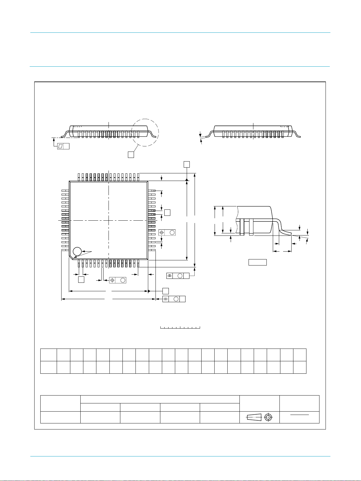
Philips Semiconductors
15. Package outline
ISP1581
USB 2.0 HS interface device
LQFP64: plastic low profile quad flat package; 64 leads; body 10 x 10 x 1.4 mm
c
y
X
A
48 33
49
64
pin 1 index
1
16
Z
32
E
e
H
E
E
w M
b
p
17
A
2
A
A
1
detail X
SOT314-2
(A )
3
θ
L
p
L
Z
e
DIMENSIONS (mm are the original dimensions)
UNIT
Note
1. Plastic or metal protrusions of 0.25 mm maximum per side are not included.
A
A1A2A3bpcE
max.
0.20
0.05
1.45
1.35
1.60
mm
OUTLINE
VERSION
SOT314-2 MS-026136E10
IEC JEDEC EIAJ
b
0.25
w M
p
D
H
D
0.27
0.17
D
0 2.5 5 mm
(1)
(1) (1)(1)
D
0.18
0.12
10.1
10.1
9.9
9.9
REFERENCES
Fig 32. LQFP64 package outline.
v M
A
B
v M
B
scale
H
eHELL
D
0.5
12.15
11.85
12.15
11.85
0.75
0.45
Zywv θ
p
0.12 0.11.0 0.2
EUROPEAN
PROJECTION
Z
1.45
1.05
D
E
1.45
7
1.05
0
ISSUE DATE
99-12-27
00-01-19
o
o
9397 750 07648
© Philips Electronics N.V. 2000. All rights reserved.
Objective specification Rev. 02 — 23 October 2000 67 of 73
Page 68

Philips Semiconductors
16. Soldering
16.1 Introduction to soldering surface mount packages
This text gives a very brief insight to a complex technology. A more in-depth account
of soldering ICs can be found in our
Packages
There is no soldering method that is ideal for all surface mount IC packages. Wave
soldering can still be used for certain surface mount ICs, but it is not suitable for fine
pitch SMDs. In these situations reflow soldering is recommended.
16.2 Reflow soldering
Reflow soldering requires solder paste (a suspension of fine solder particles, flux and
binding agent) to be applied to the printed-circuit board by screen printing, stencilling
or pressure-syringe dispensing before package placement.
Several methods exist for reflowing; for example, convection or convection/infrared
heating in a conveyor type oven. Throughput times (preheating, soldering and
cooling) vary between 100 and 200 seconds depending on heating method.
ISP1581
USB 2.0 HS interface device
Data Handbook IC26; Integrated Circuit
(document order number 9398 652 90011).
Typical reflow peak temperatures range from 215 to 250 °C. The top-surface
temperature of the packages should preferable be kept below 220 °C for thick/large
packages, and below 235 °C small/thin packages.
16.3 Wave soldering
Conventional single wave soldering is not recommended for surface mount devices
(SMDs) or printed-circuit boards with a high component density, as solder bridging
and non-wetting can present major problems.
To overcome these problems the double-wave soldering method was specifically
developed.
If wave soldering is used the following conditions must be observed for optimal
results:
Use a double-wave soldering method comprising a turbulent wave with high
•
upward pressure followed by a smooth laminar wave.
For packages with leads on two sides and a pitch (e):
•
– larger than or equal to 1.27 mm, the footprint longitudinal axis is preferred to be
parallel to the transport direction of the printed-circuit board;
– smaller than 1.27 mm, the footprint longitudinal axis must be parallel to the
transport direction of the printed-circuit board.
The footprint must incorporate solder thieves at the downstream end.
For packages with leads on four sides, the footprint must be placed at a 45° angle
•
to the transport direction of the printed-circuit board. The footprint must
incorporate solder thieves downstream and at the side corners.
9397 750 07648
Objective specification Rev. 02 — 23 October 2000 68 of 73
© Philips Electronics N.V. 2000. All rights reserved.
Page 69

Philips Semiconductors
During placement and before soldering, the package must be fixed with a droplet of
adhesive. The adhesive can be applied by screen printing, pin transfer or syringe
dispensing. The package can be soldered after the adhesive is cured.
Typical dwell time is 4 seconds at 250 °C. A mildly-activated flux will eliminate the
need for removal of corrosive residues in most applications.
16.4 Manual soldering
Fix the component by first soldering two diagonally-opposite end leads. Use a low
voltage (24 V or less) soldering iron applied to the flat part of the lead. Contact time
must be limited to 10 seconds at up to 300 °C.
When using a dedicated tool, all other leads can be soldered in one operation within
2 to 5 seconds between 270 and 320 °C.
16.5 Package related soldering information
Table 88: Suitability of surface mount IC packages for wave and reflow soldering
Package Soldering method
BGA, LFBGA, SQFP, TFBGA not suitable suitable
HBCC, HLQFP, HSQFP, HSOP, HTQFP,
HTSSOP, SMS
PLCC
LQFP, QFP, TQFP not recommended
SSOP, TSSOP, VSO not recommended
ISP1581
USB 2.0 HS interface device
methods
Wave Reflow
not suitable
[3]
, SO, SOJ suitable suitable
[2]
[3][4]
[5]
suitable
suitable
suitable
[1]
[1] All surface mount (SMD) packages are moisture sensitive. Depending upon the moisture content, the
maximum temperature (with respect to time) and body size of the package, there is a risk that internal
or external package cracks may occur due to vaporization of the moisture in them (the so called
popcorn effect). For details, refer to the Drypack information in the
Circuit Packages; Section: Packing Methods
[2] These packages are not suitable for wavesoldering as a solder joint between the printed-circuit board
and heatsink (at bottom version) can not be achieved, and as solder may stick to the heatsink (on top
version).
[3] If wave soldering is considered, then the package must be placed at a 45° angle to the solder wave
direction. The package footprint must incorporate solder thieves downstream and at the side corners.
[4] Wave soldering is only suitable for LQFP, QFP and TQFP packages with a pitch (e) equal to or larger
than 0.8 mm; it is definitely not suitable for packages with a pitch (e) equal to or smaller than 0.65 mm.
[5] Wave soldering is only suitableforSSOP and TSSOP packages with a pitch (e) equal to orlargerthan
0.65 mm; it is definitely not suitable for packages with a pitch (e) equal to or smaller than 0.5 mm.
9397 750 07648
Objective specification Rev. 02 — 23 October 2000 69 of 73
.
Data Handbook IC26; Integrated
© Philips Electronics N.V. 2000. All rights reserved.
Page 70

Philips Semiconductors
ISP1581
USB 2.0 HS interface device
17. Revision history
Table 89: Revision history
Rev Date CPCN Description
02 20001023 Objective specification; second version. Supersedes ISP1581-01 of 4 October 2000
(9397 750 07487).
Package replaced by SOT314-2.
01 20001004 Objective specification; initial version. Not published.
9397 750 07648
Objective specification Rev. 02 — 23 October 2000 70 of 73
© Philips Electronics N.V. 2000. All rights reserved.
Page 71

Philips Semiconductors
18. Data sheet status
ISP1581
USB 2.0 HS interface device
Datasheet status Product status Definition
Objective specification Development This data sheet contains the design target or goal specifications for product development. Specification may
change in any manner without notice.
Preliminary specification Qualification This data sheet contains preliminary data, and supplementary data will be published at a later date. Philips
Semiconductors reserves the right to make changes at any time without notice in order to improve design and
supply the best possible product.
Product specification Production This data sheet contains final specifications. Philips Semiconductors reserves the right to make changes at any
time without notice in order to improve design and supply the best possible product.
[1] Please consult the most recently issued data sheet before initiating or completing a design.
19. Definitions
Short-form specification — The data in a short-form specification is
extracted from a full data sheet with the same type number and title. For
detailed information see the relevant data sheet or data handbook.
Limiting values definition — Limiting values given are in accordance with
the Absolute Maximum Rating System (IEC 60134). Stress above one or
more of the limiting values may cause permanent damage to the device.
These are stress ratings only and operation of the device at these or at any
other conditions above those given in the Characteristics sections of the
specification is not implied. Exposure to limiting values for extended periods
may affect device reliability.
Application information — Applications that are described herein for any
of these products are for illustrative purposes only. Philips Semiconductors
make no representation or warranty that such applications will be suitable for
the specified use without further testing or modification.
[1]
20. Disclaimers
Life support — These products are not designed for use in life support
appliances, devices, or systems where malfunction of these products can
reasonably be expected to result in personal injury. Philips Semiconductors
customers using or selling these products for use in such applications do so
at their own risk and agree to fully indemnify Philips Semiconductors for any
damages resulting from such application.
Right to make changes — Philips Semiconductors reserves the right to
make changes, without notice, in the products, including circuits, standard
cells, and/or software, described or contained herein in order to improve
design and/or performance. Philips Semiconductors assumes no
responsibility or liability for the use of any of these products, conveys no
licence or title under any patent, copyright, or mask work right to these
products, and makes no representations or warranties that these products
are free from patent, copyright, or mask work right infringement, unless
otherwise specified.
21. Trademarks
ACPI — is an open industry specification for PC power management,
co-developed by Intel Corp., Microsoft Corp. and Toshiba
Jaz — is a registered trademark of Iomega Corp.
OnNow — is a trademark of Microsoft Corp.
SoftConnect — is a trademark of Royal Philips Electronics
Zip — is a registered trademark of Iomega Corp.
9397 750 07648
© Philips Electronics N.V. 2000 All rights reserved.
Objective specification Rev. 02 — 23 October 2000 71 of 73
Page 72

Philips Semiconductors
USB 2.0 HS interface device
Philips Semiconductors - a worldwide company
ISP1581
Argentina: see South America
Australia: Tel. +61 2 9704 8141, Fax. +61 2 9704 8139
Austria: Tel. +43 160 101, Fax. +43 160 101 1210
Belarus: Tel. +375 17 220 0733, Fax. +375 17 220 0773
Belgium: see The Netherlands
Brazil: see South America
Bulgaria: Tel. +359 268 9211, Fax. +359 268 9102
Canada: Tel. +1 800 234 7381
China/Hong Kong: Tel. +852 2 319 7888, Fax. +852 2 319 7700
Colombia: see South America
Czech Republic: see Austria
Denmark: Tel. +45 3 288 2636, Fax. +45 3 157 0044
Finland: Tel. +358 961 5800, Fax. +358 96 158 0920
France: Tel. +33 14 099 6161, Fax. +33 14 099 6427
Germany: Tel. +49 40 23 5360, Fax. +49 402 353 6300
Hungary: see Austria
India: Tel. +91 22 493 8541, Fax. +91 22 493 8722
Indonesia: see Singapore
Ireland: Tel. +353 17 64 0000, Fax. +353 17 64 0200
Israel: Tel. +972 36 45 0444, Fax. +972 36 49 1007
Italy: Tel. +39 039 203 6838, Fax +39 039 203 6800
Japan: Tel. +81 33 740 5130, Fax. +81 3 3740 5057
Korea: Tel. +82 27 09 1412, Fax. +82 27 09 1415
Malaysia: Tel. +60 37 50 5214, Fax. +60 37 57 4880
Mexico: Tel. +9-5 800 234 7381
Middle East: see Italy
Netherlands: Tel. +31 40 278 2785, Fax. +31 40 278 8399
New Zealand: Tel. +64 98 49 4160, Fax. +64 98 49 7811
Norway: Tel. +47 22 74 8000, Fax. +47 22 74 8341
Philippines: Tel. +63 28 16 6380, Fax. +63 28 17 3474
Poland: Tel. +48 22 5710 000, Fax. +48 22 5710 001
Portugal: see Spain
Romania: see Italy
Russia: Tel. +7 095 755 6918, Fax. +7 095 755 6919
Singapore: Tel. +65 350 2538, Fax. +65 251 6500
Slovakia: see Austria
Slovenia: see Italy
South Africa: Tel. +27 11 471 5401, Fax. +27 11 471 5398
South America: Tel. +55 11 821 2333, Fax. +55 11 829 1849
Spain: Tel. +34 33 01 6312, Fax. +34 33 01 4107
Sweden: Tel. +46 86 32 2000, Fax. +46 86 32 2745
Switzerland: Tel. +41 14 88 2686, Fax. +41 14 81 7730
Taiwan: Tel. +886 22 134 2451, Fax. +886 22 134 2874
Thailand: Tel. +66 23 61 7910, Fax. +66 23 98 3447
Turkey: Tel. +90 216 522 1500, Fax. +90 216 522 1813
Ukraine: Tel. +380 44 264 2776, Fax. +380 44 268 0461
United Kingdom: Tel. +44 208 730 5000, Fax. +44 208 754 8421
United States: Tel. +1 800 234 7381
Uruguay: see South America
Vietnam: see Singapore
Yugoslavia: Tel. +381 11 3341 299, Fax. +381 11 3342 553
For all other countries apply to: Philips Semiconductors,
Marketing Communications,
Building BE, P.O. Box 218, 5600 MD EINDHOVEN,
The Netherlands, Fax. +31 40 272 4825
Internet: http://www.semiconductors.philips.com
(SCA70)
9397 750 07648
Objective specification Rev. 02 — 23 October 2000 72 of 73
© Philips Electronics N.V. 2000. All rights reserved.
Page 73

Philips Semiconductors
Contents
ISP1581
USB 2.0 HS interface device
1 General description . . . . . . . . . . . . . . . . . . . . . . 1
2 Features . . . . . . . . . . . . . . . . . . . . . . . . . . . . . . . 2
3 Applications . . . . . . . . . . . . . . . . . . . . . . . . . . . . 2
4 Ordering information. . . . . . . . . . . . . . . . . . . . . 2
5 Block diagram . . . . . . . . . . . . . . . . . . . . . . . . . . 3
6 Pinning information. . . . . . . . . . . . . . . . . . . . . . 4
6.1 Pinning . . . . . . . . . . . . . . . . . . . . . . . . . . . . . . . 4
6.2 Pin description . . . . . . . . . . . . . . . . . . . . . . . . . 5
7 Functional description . . . . . . . . . . . . . . . . . . . 7
7.1 USB 2.0 transceiver . . . . . . . . . . . . . . . . . . . . . 8
7.2 Philips Serial Interface Engine (SIE). . . . . . . . . 9
7.3 Voltage regulators. . . . . . . . . . . . . . . . . . . . . . . 9
7.4 Memory Management Unit (MMU) and
integrated RAM . . . . . . . . . . . . . . . . . . . . . . . . 9
7.5 SoftConnect . . . . . . . . . . . . . . . . . . . . . . . . . . . 9
7.6 Bit clock recovery . . . . . . . . . . . . . . . . . . . . . . . 9
7.7 Multiplying PLL oscillator . . . . . . . . . . . . . . . . . 9
7.8 Microcontroller Interface and
Microcontroller Handler . . . . . . . . . . . . . . . . . 10
7.9 DMA Interface and DMA Handler. . . . . . . . . . 10
7.10 System Controller. . . . . . . . . . . . . . . . . . . . . . 10
8 Modes of operation . . . . . . . . . . . . . . . . . . . . . 11
9 Register descriptions . . . . . . . . . . . . . . . . . . . 11
9.1 Register access . . . . . . . . . . . . . . . . . . . . . . . 13
9.2 Initialization registers . . . . . . . . . . . . . . . . . . . 13
9.2.1 Address register (address: 00H). . . . . . . . . . . 13
9.2.2 Mode register (address: 0CH) . . . . . . . . . . . . 14
9.2.3 Interrupt Configuration register (address: 10H) 15
9.2.4 Interrupt Enable register (address: 14H) . . . . 16
9.2.5 DMA Configuration register (address: 38H) . . 17
9.2.6 DMA Hardware register (address: 3CH). . . . . 17
9.3 Data flow registers . . . . . . . . . . . . . . . . . . . . . 18
9.3.1 Endpoint Index register (address: 2CH) . . . . . 18
9.3.2 Control Function register (address: 28H) . . . . 19
9.3.3 Data Port register (address: 20H). . . . . . . . . . 19
9.3.4 Buffer Length register (address: 1CH) . . . . . . 20
9.3.5 Endpoint MaxPacketSize register (address:
04H). . . . . . . . . . . . . . . . . . . . . . . . . . . . . . . . 21
9.3.6 Endpoint Type register (address: 08C). . . . . . 22
9.3.7 Short Packet register (address: 24H) . . . . . . . 22
9.4 DMA registers. . . . . . . . . . . . . . . . . . . . . . . . . 24
9.4.1 DMA Command register (address: 30H) . . . . 26
9.4.2 DMA Transfer Counter register (address: 34H) 27
9.4.3 DMA Configuration register (address: 38H) . . 28
9.4.4 DMA Hardware register (address: 3CH). . . . . 30
9.4.5 DMA Strobe Timing register (address: 60H). . 31
9.4.6 Task File registers (addresses: 40H to 4FH) . 32
9.4.7 DMA Interrupt Reason register (address: 50H) 35
9.4.8 DMA Interrupt Enable register (address: 54H) 36
9.4.9 DMA Endpoint register (address: 58H). . . . . . 36
9.5 General registers . . . . . . . . . . . . . . . . . . . . . . 37
9.5.1 Interrupt register (address: 18H). . . . . . . . . . . 37
9.5.2 Chip ID register (address: 70H) . . . . . . . . . . . 38
9.5.3 Frame Number register (address: 74H) . . . . . 39
9.5.4 Scratch register (address: 78H) . . . . . . . . . . . 40
9.5.5 Unlock Device register (address: 7CH). . . . . . 40
9.5.6 Test Mode register (address: 84H) . . . . . . . . . 41
10 Limiting values . . . . . . . . . . . . . . . . . . . . . . . . . 42
11 Static characteristics . . . . . . . . . . . . . . . . . . . . 42
12 Dynamic characteristics . . . . . . . . . . . . . . . . . 44
12.1 High-speed signals . . . . . . . . . . . . . . . . . . . . . 46
12.1.1 Template 1 (transmit waveform; device
without captive cable) . . . . . . . . . . . . . . . . . . 47
12.1.2 Template 2 (transmit waveform; device
with captive cable) . . . . . . . . . . . . . . . . . . . . 48
12.1.3 Template 3 (receive waveform; receiver
sensitivity with captive cable). . . . . . . . . . . . . 49
12.1.4 Template 4 (receive waveform; receiver
sensitivity without captive cable) . . . . . . . . . . 50
12.2 Timing symbols. . . . . . . . . . . . . . . . . . . . . . . . 51
12.3 Parallel I/O timing . . . . . . . . . . . . . . . . . . . . . . 52
12.3.1 Generic Processor mode (BUS_CONF = 1). . 52
12.3.2 Split Bus mode (BUS_CONF = 0). . . . . . . . . . 53
12.4 DMA timing . . . . . . . . . . . . . . . . . . . . . . . . . . . 54
12.4.1 PIO mode . . . . . . . . . . . . . . . . . . . . . . . . . . . . 54
12.4.2 GDMA slave mode . . . . . . . . . . . . . . . . . . . . . 56
12.4.3 MDMA mode. . . . . . . . . . . . . . . . . . . . . . . . . . 59
12.4.4 UDMA mode . . . . . . . . . . . . . . . . . . . . . . . . . . 60
13 Application information. . . . . . . . . . . . . . . . . . 65
14 Test information . . . . . . . . . . . . . . . . . . . . . . . . 66
15 Package outline . . . . . . . . . . . . . . . . . . . . . . . . 67
16 Soldering. . . . . . . . . . . . . . . . . . . . . . . . . . . . . . 68
16.1 Introduction to soldering surface mount
packages . . . . . . . . . . . . . . . . . . . . . . . . . . . . 68
16.2 Reflow soldering . . . . . . . . . . . . . . . . . . . . . . . 68
16.3 Wave soldering. . . . . . . . . . . . . . . . . . . . . . . . 68
16.4 Manual soldering. . . . . . . . . . . . . . . . . . . . . . . 69
16.5 Package related soldering information . . . . . . 69
17 Revision history . . . . . . . . . . . . . . . . . . . . . . . . 70
18 Data sheet status . . . . . . . . . . . . . . . . . . . . . . . 71
19 Definitions. . . . . . . . . . . . . . . . . . . . . . . . . . . . . 71
20 Disclaimers. . . . . . . . . . . . . . . . . . . . . . . . . . . . 71
21 Trademarks. . . . . . . . . . . . . . . . . . . . . . . . . . . . 71
© Philips Electronics N.V. 2000. Printed in The Netherlands
All rights are reserved. Reproduction in whole or in part is prohibited without the prior
written consent of the copyright owner.
The information presented in this document does not form part of any quotation or
contract, is believed to be accurate and reliable and may be changed without notice. No
liability will be accepted by the publisher for any consequence of its use. Publication
thereof does not convey nor imply any license under patent- or other industrial or
intellectual property rights.
Date of release: 23 October 2000 Document order number: 9397 750 07648
 Loading...