

Page 1
®
ISO175
Precision, Isolated
INSTRUMENT ATION AMPLIFIER
ISO175
FEATURES
● RATED
1500Vrms Continuous
2500Vrms for One Minute
100% TESTED FOR PARTIAL DISCHARGE
● HIGH IMR: 115dB at 50Hz
● LOW NONLINEARITY:
±0.01%
● LOW INPUT BIAS CURRENT: 10nA max
● LOW INPUT OFFSET VOLTAGE: 101mV max
● INPUTS PROTECTED TO
● BIPOLAR OPERATION: V
±40V
= ±10V
O
● SYNCHRONIZATION CAPABILITY
● 24-PIN PLASTIC DIP: 0.3" Wide
APPLICATIONS
● INDUSTRIAL PROCESS CONTROL
Transducer Isolator, Thermocouple
Isolator, RTD Isolator, Pressure Bridge
Isolator, Flow Meter Isolator
● POWER MONITORING
● MEDICAL INSTRUMENTATION
● ANALYTICAL MEASUREMENTS
● BIOMEDICAL MEASUREMENTS
● DATA ACQUISITION
● TEST EQUIPMENT
● POWER MONITORING
● GROUND LOOP ELIMINATION
V
1
IN–
R
22
G
2
R
G
24
V
IN+
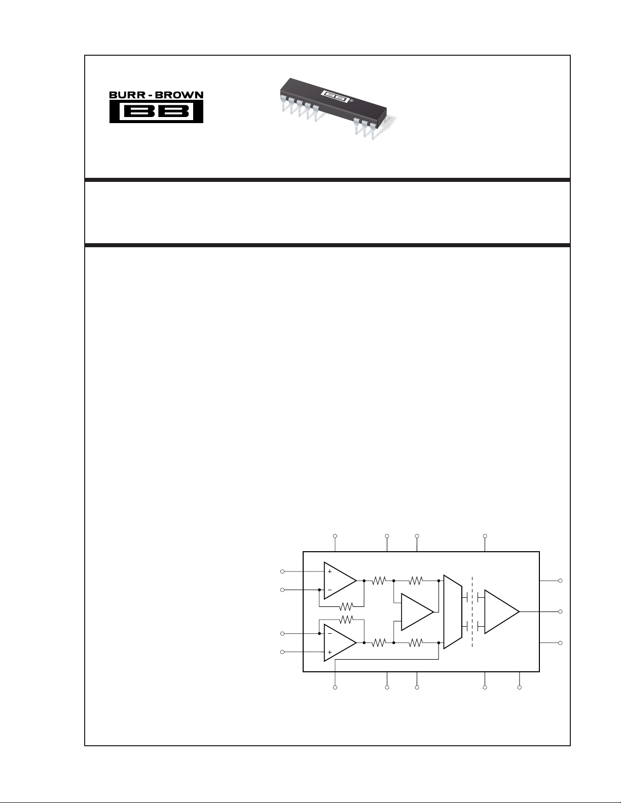
DESCRIPTION
ISO175 is a precision isolated instrumentation amplifier incorporating a novel duty cycle modulationdemodulation technique and excellent accuracy. A
single external resistor sets the gain. Internal input
protection can withstand up to ±40V without damage.
The signal is transmitted digitally across a differential
capacitive barrier. With digital modulation the barrier
characteristics do not affect signal integrity. This results in excellent reliability and good high frequency
transient immunity across the barrier. Both the amplifier and barrier capacitors are housed in a plastic DIP.
ISO175 is easy to use. A power supply range of ±4.5V
to ±18V makes this amplifier ideal for a wide range of
applications.
5214 15
Shield 1 Ext Osc +V
S1
+V
S2
Shield 2
V
OUT
Com2
14
11
10
Com1
23 20 3 13 12
International Airport Industrial Park • Mailing Address: PO Box 11400, Tucson, AZ 85734 • Street Address: 6730 S. Tucson Blvd., Tucson, AZ 85706 • Tel: (520) 746-1111 • Twx: 910-952-1111
Internet: http://www.burr-brown.com/ • FAXLine: (800) 548-6133 (US/Canada Only) • Cable: BBRCORP • Telex: 066-6491 • FAX: (520) 889-1510 • Immediate Product Info: (800) 548-6132
©
1996 Burr-Brown Corporation PDS-1293A Printed in U.S.A. May, 1996
GND1 –V
S1
–V
GND2
S2
Page 2
SPECIFICATIONS
At TA = +25°C, VS1 = VS2 = ±15V, and RL = 2kΩ unless otherwise noted.
ISO175P
PARAMETER CONDITIONS MIN TYP MAX UNITS
ISOLATION
Voltage Rated Continuous:
AC T
DC T
100% Test (AC, 50Hz) 1s; Partial Discharge ≤ 5pC 2500 Vrms
Isolation-Mode Rejection
AC 50Hz 1500Vrms 115 dB
DC 160 dB
Barrier Impedance 10
Leakage Current VISO = 240Vrms, 50Hz 0.8 1 µArms
GAIN
Gain Error G = 1 ±0.35 %
Gain vs Temperature G = 1 ±11 ppm/°C
Nonlinearity G = 1 ±0.102 %
INPUT OFFSET VOLTAGE
Initial Offset G = 1, 100 mV
vs Temperature µV/°C
vs Supply G = 1 ±2 mV/V
INPUT
Voltage Range ±10 V
Bias Current ±10 nA
vs Temperature ±40 pA/°C
Offset Current ±10 nA
vs Temperature ±40 pA/°C
OUTPUT
Voltage Range ±10 V
Current Drive ±5mA
Capacitive Load Drive 0.1 µF
Ripple Voltage 10 mVp-p
FREQUENCY RESPONSE
Small Signal Bandwidth G = 1 60 kHz
Slew Rate V
POWER SUPPLIES
Rated Voltage 15 V
Voltage Range ±4.5 ±18 V
Quiescent Current
V
V
TEMPERATURE RANGE
Operating –40 85 °C
Storage –40 125 °C
NOTE: (1) All devices receive a 1s test. Failure criterion is ≥ 5 pulses of ≥ 5pc.
(1)
MIN
MIN
to T
to T
MAX
MAX
1500 Vrms
2121 VDC
14
|| 6 Ω || pF
50k
1+
R
G
V/V
G = 10 ±0.07 %
G = 100 ±0.95 %
G = 10 ±0.04 %
G = 100 ±0.104 %
101
± 1+
520
G
± 0.125 +
G
G = 10 60 kHz
G = 100 50 kHz
= ±10V, G = 10 0.9 V/µs
O
S1
S2
±7.4 mA
±7.5 mA
®
ISO175
2
Page 3
V
S1–
V
S1+
Shield 1
Com 2
V
OUT
GND 2
R
G
EXT OSC
GND 1
V
S2+
Shield 2
V
S2–
R
G
Com 1
V
IN–
1
2
3
4
5
10
11
12
24
23
22
21
20
15
14
13
V
IN+
ABSOLUTE MAXIMUM RATINGS
Supply Voltage................................................................................... ±18V
Analog Input Voltage Range .............................................................. ±40V
External Oscillator Input..................................................................... ±25V
Com 1 to GND1 ................................................................................... ±1V
Com 2 to GND2 ................................................................................... ±1V
Continuous Isolation Voltage: ....................................................1500Vrms
IMV, dv/dt...................................................................................... 20kV/µs
Junction Temperature ...................................................................... 150°C
Storage Temperature...................................................... –40°C to +125°C
Lead Temperature (soldering, 10s)................................................ +300°C
Output Short Duration .......................................... Continuous to Common
ELECTROSTATIC
DISCHARGE SENSITIVITY
Any integrated circuit can be damaged by ESD. Burr-Brown
recommends that all integrated circuits be handled with
appropriate precautions. Failure to observe proper handling
and installation procedures can cause damage.
ESD damage can range from subtle performance degradation to complete device failure. Precision integrated circuits
may be more susceptible to damage because very small
parametric changes could cause the device not to meet
published specifications.
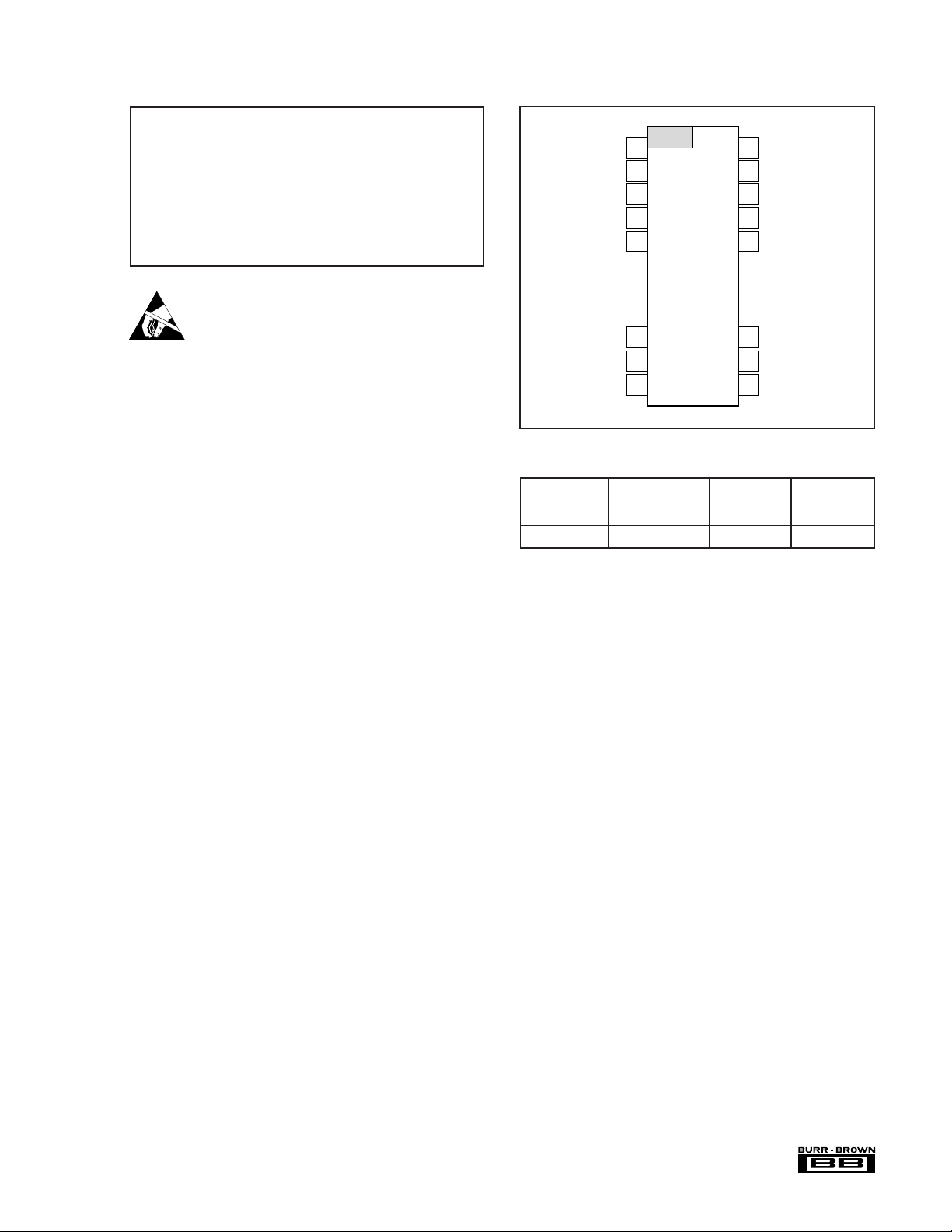
PIN CONFIGURATION
PACKAGE/ORDERING INFORMATION
PACKAGE
DRAWING
PRODUCT PACKAGE NUMBER
ISO175P 24-Pin Plastic DIP 243-2 60kHz
NOTE: (1) For detailed drawing and dimension table, please see end of data
sheet, or Appendix C of Burr-Brown IC Data Book.
(1)
BANDWIDTH
The information provided herein is believed to be reliable; however, BURR-BROWN assumes no responsibility for inaccuracies or omissions. BURR-BROWN assumes
no responsibility for the use of this information, and all use of such information shall be entirely at the user's own risk. Prices and specifications are subject to change
without notice. No patent rights or licenses to any of the circuits described herein are implied or granted to any third party. BURR-BROWN does not authorize or warrant
any BURR-BROWN product for use in life support devices and/or systems.
3
ISO175
®
Page 4
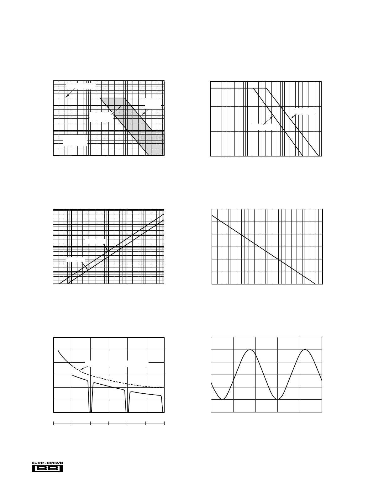
TYPICAL PERFORMANCE CURVES
At TA = +25°C, VS1 = VS2 = ±15V, and RL = 2kΩ, unless otherwise noted.
ISOLATION MODE VOLTAGE
vs FREQUENCY
Max DC Rating
2k
1k
100
Peak Isolation Voltage
Typical
Performance
Degraded
Performance
Max AC
Rating
60
54
40
PSRR (dB)
20
PSRR vs FREQUENCY
–VS1, –V
S2
+VS1, +V
S2
10
100
1k 100k 10M
100mA
10mA
1mA
100µA
10µA
Leakage Current (rms)
1µA
240 Vrms
0.1µA
1
SIGNAL RESPONSE vs CARRIER FREQUENCY
10k 1M 100M
Frequency (Hz)
ISOLATION LEAKAGE CURRENT
vs FREQUENCY
1500 Vrms
100 10k 1M10 1k 100k
Frequency (Hz)
0
160
140
120
100
IMR (dB)
80
60
40
15
1
100 10k 1M
10 1k 100k
Frequency (Hz)
IMR vs FREQUENCY
1
100 10k 1M10 1k 100k
Frequency (Hz)
SINE RESPONSE ISO175
(f = 2kHz, Gain = 10)
0
(dB)
IN
–20
/V
OUT
V
–40
0
(Hz)
f
IN
f
(Hz)
0000f
OUT
®
–20dB/dec (for comparison only)
f
C
/2 fC/2 fC/2
c
2f
C
ISO175
10
5
0
–5
Output Voltage (V)
–10
–15
3f
C
0
400 1000200 600 800
Time (µs)
4
Page 5

GAIN vs FREQUENCY
80
60
40
20
0
–20
Gain (dB)
Frequency (Hz)
1k 10k 100k
G = 100
G = 10
G = 1
G = 1000
0
Time (µs)
10
5
0
–5
–10
–15
Output Voltage (V)
15
10
5
0
–5
–10
Input Voltage (V)
200 500100 300 400
STEP RESPONSE
TYPICAL PERFORMANCE CURVES (CONT)
At TA = +25°C, VS1 = VS2 = ±15V, and RL = 2kΩ, unless otherwise noted.
SINE RESPONSE
15
10
5
0
–5
Output Voltage (V)
–10
–15
0
(f = 20kHz, Gain = 10)
400 1000200 600 800
Time (µs)
10
5
0
–5
–10
Output Voltage (V)
–15
0
INPUT COMMON-MODE RANGE
15
G ≥ 10
10
G = 1 G = 1
5
0
V
V
–5
Common-Mode Voltage (V)
–10
–15
–15 –10 0 5 15–5
All
Gains
STEP RESPONSE
40 10020 60 80
Time (µs)
vs OUTPUT VOLTAGE
–
D/2
+
–
D/2
+
V
CM
Output Voltage (V)
G ≥ 10
V
O
All
Gains
10
15
10
5
0
–5
Input Voltage (V)
–10
5
INPUT BIAS AND OFFSET CURRENT
vs TEMPERATURE
5
4
3
2
1
I
OS
±I
b
0
–1
–2
–3
Input Bias and Offset Current (nA)
–4
–5
–75 –50 –25 0 25 50 75 100 125
Temperature (°C)
ISO175
®
Page 6
BASIC OPERATION
ISO175 instrumentation input isolation amplifier comprises
of a precision instrumentation amplifier followed by an
isolation amplifier. The input and output isolation sections
are galvanically isolated and EMI shielded by matched
capacitors.
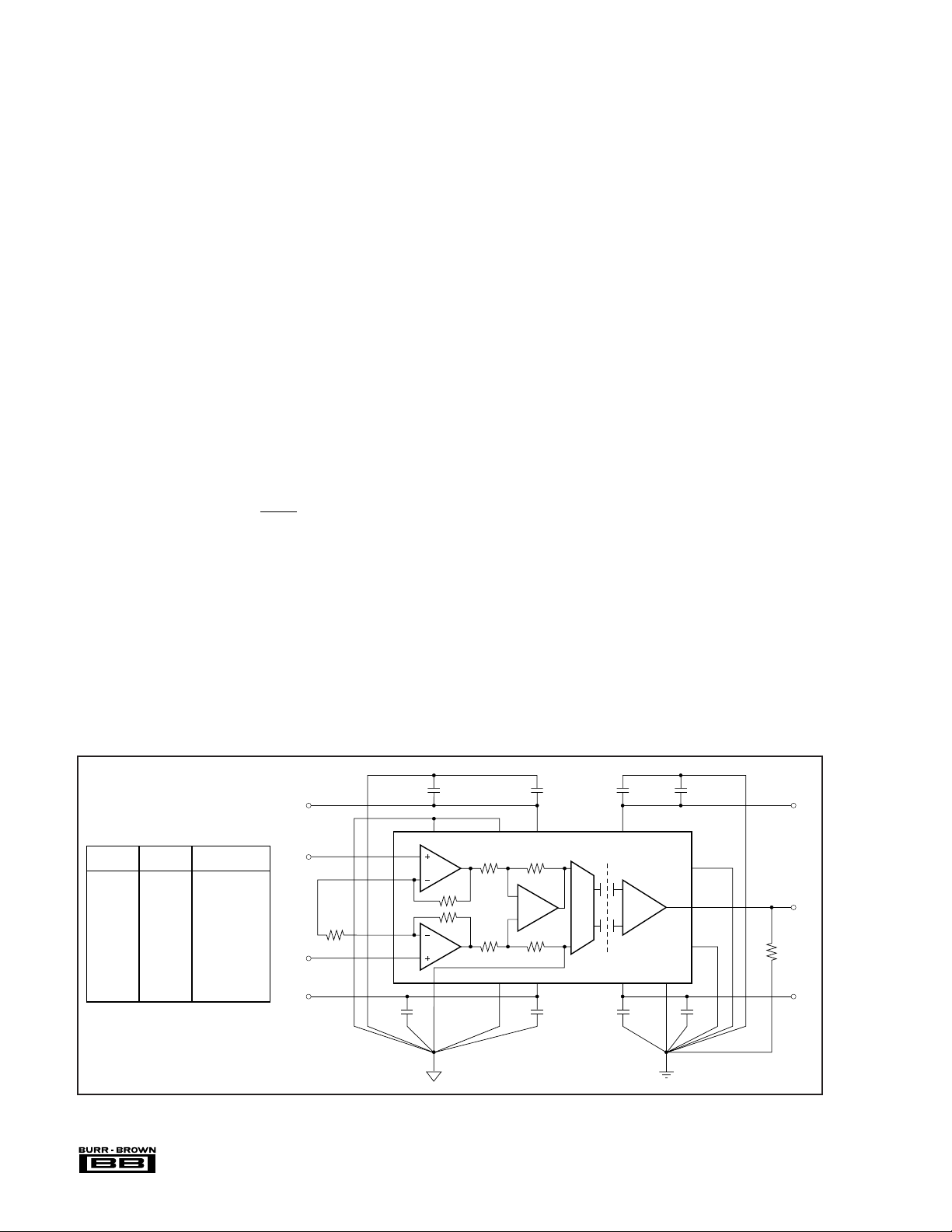
Signal and Power Connections
Figure 1 shows power and signal connections. Each power
supply pin should be bypassed with a 1µF tantalum capacitor located as close to the amplifier as possible. All ground
connections should be run independently to a common point
if possible. Signal Common on both input and output sections provide a high-impedance point for sensing signal
ground in noisy applications. Com 1 and Com 2 must have
a path to ground for bias current return and should be
maintained within ±1V of GND1 and GND2, respectively.
SETTING THE GAIN
Gain of the ISO175 is set by connecting a single external
resistor R
, connected between pins 2 and 22.
G
G = 1 +
50 kΩ
R
G
(1)
Commonly used gains and resistor values are shown in
Figure 1.
The 50kΩ term in equation (1) comes from the sum of the
two internal feedback resistors. These on-chip metal film
resistors are laser trimmed to accurate absolute values. The
accuracy and temperature coefficient of this resistor are
included in the gain accuracy and drift specifications of the
ISO175.
The stability and temperature drift of the external gain
setting resistor R
, also affects gain. RG’s contribution to
G
gain accuracy and drift can be directly inferred from the
gain equation (1). Low resistor values required for high
gain can make wiring resistance important. Sockets add to
the wiring resistance which will contribute additional gain
error (possibly an unstable gain error) in gains of approximately 100 or greater.
INPUT COMMON-MODE RANGE
The linear voltage range of the input circuitry of the ISO175
is from approximately 2.5V below the positive supply voltage to 2.5V above the negative supply. As a differential
input voltage causes the output voltage to increase, however,
the linear input range will be limited by the output voltage
swing of the internal amplifiers. Thus, the linear commonmode input range is related to the output voltage of the
complete input amplifier.
This behavior also depends on the supply voltage—see
performance curves “Input Common-Mode Range vs Output Voltage.”
Input-overload can produce an output voltage that appears
normal. For example, if an input overload condition drives
both input amplifiers to their positive output swing limit, the
difference voltage measured by the output amplifier will be
near zero. The output of the ISO175 will be near 0V even
though both inputs are overloaded.
INPUT PROTECTION
The input of the ISO175 is individually protected for voltages up to ±40V referenced to GND1. For example, a
condition of –40V on one input and +40V on the other input
will not cause damage. Internal circuitry on each input
provides low series impedance under normal signal conditions. To provide equivalent protection, series input resistors
would contribute excessive noise. If the input is overloaded,
DESIRED
GAIN
1
2
8
10
20
50
100
200
500
1000
2000
6000
10000
NOTE: (1) No Connection.
R
(Ω)
NC
50.00k
12.50k
5.556k
2.632k
1.02k
505.1
251.2
100.2
50.05
25.01
10.00
5.001
G
(1)
NEAREST 1% R
(Ω)
(1)
NC
49.9k
12.4k
5.62k
2.61k
1.02k
511
249
100
49.9
24.9
10
4.99
FIGURE 1. Basic Connections.
®
ISO175
+V
S1
V
G
IN–
R
G
V
IN+
–V
S1
1
22
2
24
0.1µF
0.1µF 1µF
521
Shield 1 Ext Osc +V
Com 1
23 20 3 13 12
GND 1
+
415
S1
–V
S1
1µF
+
1µF 0.1µF
+
+V
S2
–V
GND 2
S2
1µF
+
Shield 2
V
Com2
+V
S2
14
11
OUT
10
0.1µF
V
OUT
R
LOAD
–V
S2
6
Page 7

the protection circuitry limits the input current to a safe
value of approximately 1.5 to 5mA. The inputs are protected
even if the power supplies are disconnected or turned off.
SYNCHRONIZED OPERATION
ISO175 can be synchronized to an external signal source.
This capability is useful in eliminating troublesome beat
frequencies in multichannel systems and in rejecting AC
signals and their harmonics. To use this feature, an external
signal must be applied to the Ext Osc pin. ISO175 can be
synchronized over the 400kHz to 700kHz range.
The ideal external clock signal for the ISO175 is a ±4V sine
wave or ±4V, 50% duty-cycle triangle wave. The Ext Osc
pin of the ISO175 can be driven directly with a ±3V to ±5V
sine or 25% to 75% duty-cycle triangle wave and the ISO
amp’s internal modulator/demodulator circuitry will synchronize to the signal.
ISO175 can also be synchronized to a 400kHz to 700kHz
Square-Wave External Clock since an internal clamp and
filter provide signal conditioning. A square-wave signal of
25% to 75% duty cycle, and ±3V to ±20V level can be used
to directly drive the ISO175.
With the addition of the signal conditioning circuit shown in
Figure 2, any 10% to 90% duty-cycle square-wave signal
can be used to drive the ISO175 Ext Osc pin. With the values
shown, the circuit can be driven by a 4Vp-p TTL signal. For
a higher or lower voltage input, increase or decrease the 1kΩ
resistor, R
(8Vp-p) R
, proportionally, e.g. for a ±4V square-wave
X
should be increased to 2kΩ. The value of C
X
used in the Figure 2 circuit depends on the frequency of the
external clock signal. C
1µF
Sq Wave In
should be 30pF for ISO175.
X
10kΩ
C
R
1kΩ
X
X
OPA602
Triangle Out
ISO175
Ext Osc
generates an output signal component that varies in both
amplitude and frequency, as shown by the lower curve. The
lower horizontal scale shows the periodic variation in the
frequency of the output component. Note that at the carrier
frequency and its harmonics, both the frequency and amplitude of the response go to zero. These characteristics can be
exploited in certain applications.
It should be noted that for the ISO175, the carrier frequency
is nominally 500kHz and the –3dB point of the amplifier is
60kHz. Spurious signals at the output are not significant
under these circumstances unless the input signal contains
significant components above 250kHz.
When periodic noise from external sources such as system
clocks and DC/DC converters are a problem, ISO175 can
be used to reject this noise. The amplifier can be synchronized to an external frequency source, f
EXT
amplifier response curve at one of the frequency and
amplitude nulls indicated in the “Signal Response vs Carrier Frequency” performance curve. Figure 3 shows circuitry with opto-isolation suitable for driving the Ext Osc
input from TTL levels.
+15V+5V
200Ω
X
TTL
f
IN
3
6N136
2.5kΩ
C
82
2.5kΩ
6
10kΩ
5
= 10 X C1, with a minimum 10nF
C
2
2
C
1
140E-6
C1 = – 350pF
()
FIGURE 3. Synchronization with Isolated Drive Circuit for
Ext Osc Pin.
, placing the
Ext Osc on
ISO175
(Pin 21)
f
IN
FIGURE 2. Square-Wave to Triangle Wave Signal Condi-
tioner for Driving ISO175 Ext Osc Pin.
CARRIER FREQUENCY CONSIDERATIONS
ISO175 amplifier transmit the signal across the ISO-barrier
by a duty-cycle modulation technique. This system works
like any linear amplifier for input signals having frequencies
below one half the carrier frequency, f
cies above f
/2, the behavior becomes more complex. The
C
. For signal frequen-
C
“Signal Response vs Carrier Frequency” performance curve
describes this behavior graphically. The upper curve illustrates the response for input signals varying from DC to
fC/2. At input frequencies at or above fC/2, the device
ISOLATION MODE VOLTAGE
Isolation Mode Voltage (IMV) is the voltage appearing
between isolated grounds GND1 and GND2. The IMV can
induce errors at the output as indicated by the plots of IMV
versus Frequency. It should be noted that if the IMV frequency exceeds f
/2, the output will display spurious out-
C
puts in a manner similar to that described above, and the
amplifier response will be identical to that shown in the
“Signal Response vs Carrier Frequency” performance curve.
This occurs because IMV-induced errors behave like inputreferred error signals. To predict the total IMR, divide the
isolation voltage by the IMR shown in “IMR vs Frequency”
performance curve and compute the amplifier response to
this input-referred error signal from the data given in the
“Signal Response vs Carrier Frequency” performance curve.
7
ISO175
®
Page 8

Due to effects of very high-frequency signals, typical IMV
performance can be achieved only when dV/dT of the
isolation mode voltage falls below 1000V/µs. For convenience, this is plotted in the typical performance curve
for the ISO175 as a function of voltage and frequency for
sinusoidal voltages. When dV/dT exceeds 1000V/µs but
falls below 20kV/µs, performance may be degraded. At rates
of change above 20kV/µs, the amplifier may be damaged,
but the barrier retains its full integrity. Lowering the power
supply voltages below ±15V may decrease the dV/dT to
500V/µs for typical performance, but the maximum dV/dT
of 20kV/µs remains unchanged.
Leakage current is determined solely by the impedance of
the barrier capacitance and is plotted in the “Isolation Leakage Current vs Frequency” curve.
ISOLATION VOLTAGE RATINGS
Because a long-term test is impractical in a manufacturing
situation, the generally accepted practice is to perform a
production test at a higher voltage for some shorter time.
The relationship between actual test voltage and the continuous derated maximum specification is an important one.
Historically, Burr-Brown has chosen a deliberately conservative one: VTEST = (2 x ACrms continuous rating) +
1000V for 10 seconds, followed by a test at rated ACrms
voltage for one minute. This choice was appropriate for
conditions where system transients are not well defined.
Recent improvements in high-voltage stress testing have
produced a more meaningful test for determining maximum
permissible voltage ratings, and Burr-Brown has chosen to
apply this new technology in the manufacture and testing of
the ISO175.
PARTIAL DISCHARGE
When an insulation defect such as a void occurs within an
insulation system, the defect will display localized corona or
ionization during exposure to high-voltage stress. This ionization requires a higher applied voltage to start the
discharge and lower voltage to maintain it or extinguish it
once started. The higher start voltage is known as the
inception voltage, while the extinction voltage is that level
of voltage stress at which the discharge ceases. Just as the
total insulation system has an inception voltage, so do the
individual voids. A voltage will build up across a void until
its inception voltage is reached, at which point the void will
ionize, effectively shorting itself out. This action redistributes electrical charge within the dielectric and is known as
partial discharge. If, as is the case with AC, the applied
voltage gradient across the device continues to rise, another
partial discharge cycle begins. The importance of this
phenomenon is that, if the discharge does not occur, the
insulation system retains its integrity. If the discharge
begins, and is allowed to continue, the action of the ions and
electrons within the defect will eventually degrade any
organic insulation system in which they occur. The measurement of partial discharge is still useful in rating the devices
and providing quality control of the manufacturing process.
The inception voltage for these voids tends to be constant, so
that the measurement of total charge being redistributed
within the dielectric is a very good indicator of the size of the
voids and their likelihood of becoming an incipient failure.
The bulk inception voltage, on the other hand, varies with
the insulation system, and the number of ionization defects
and directly establishes the absolute maximum voltage (transient) that can be applied across the test device before
destructive partial discharge can begin. Measuring the bulk
extinction voltage provides a lower, more conservative voltage from which to derive a safe continuous rating. In
production, measuring at a level somewhat below the expected inception voltage and then derating by a factor
related to expectations about system transients is an accepted practice.
PARTIAL DISCHARGE TESTING
Not only does this test method provide far more qualitative
information about stress-withstand levels than did previous
stress tests, but it provides quantitative measurements from
which quality assurance and control measures can be based.
Tests similar to this test have been used by some manufacturers, such as those of high-voltage power distribution
equipment, for some time, but they employed a simple
measurement of RF noise to detect ionization. This method
was not quantitative with regard to energy of the discharge,
and was not sensitive enough for small components such as
isolation amplifiers. Now, however, manufacturers of HV
test equipment have developed means to quantify partial
discharge. VDE in Germany, an acknowledged leader in
high-voltage test standards, has developed a standard test
method to apply this powerful technique. Use of partial
discharge testing is an improved method for measuring the
integrity of an isolation barrier.
To accommodate poorly-defined transients, the part under
test is exposed to voltage that is 1.6 times the continuousrated voltage and must display less than or equal to 5pC
partial discharge level in a 100% production test.
APPLICATIONS
The ISO175 isolation amplifier is used in three categories of
applications:
• Accurate isolation of signals from high voltage ground
potentials,
• Accurate isolation of signals from severe ground noise and,
• Fault protection from high voltages in analog measurements.
®
ISO175
8
 Loading...