


1
®
ISO124
FEATURES
● 100% TESTED FOR HIGH-VOLTAGE
BREAKDOWN
● RATED 1500Vrms
● HIGH IMR: 140dB at 60Hz
● 0.010% max NONLINEARITY
● BIPOLAR OPERATION: V
O
= ±10V
● 16-PIN PLASTIC DIP AND 28-LEAD SOIC
● EASE OF USE: Fixed Unity Gain
Configuration
●
±4.5V to ±18V SUPPLY RANGE
APPLICATIONS
● INDUSTRIAL PROCESS CONTROL:
Transducer Isolator, Isolator for Thermocouples, RTDs, Pressure Bridges, and
Flow Meters, 4mA to 20mA Loop Isolation
● GROUND LOOP ELIMINATION
● MOTOR AND SCR CONTROL
● POWER MONITORING
● PC-BASED DATA ACQUISITION
● TEST EQUIPMENT
ISO124
DESCRIPTION
The ISO124 is a precision isolation amplifier incorporating a novel duty cycle modulation-demodulation
technique. The signal is transmitted digitally across
a 2pF differential capacitive barrier. With digital modulation the barrier characteristics do not affect signal
integrity, resulting in excellent reliability and good high
frequency transient immunity across the barrier. Both
barrier capacitors are imbedded in the plastic body of
the package.
The ISO124 is easy to use. No external components
are required for operation. The key specifications are
0.010% max nonlinearity, 50kHz signal bandwidth,
and 200µV/°C V
OS
drift. A power supply range of
±4.5V to ±18V and quiescent currents of ±5.0mA on
V
S1
and ±5.5mA on VS2 make these amplifiers ideal
for a wide range of applications.
The ISO124 is available in 16-pin plastic DIP and 28-
lead plastic surface mount packages.
®
Precision Lowest Cost
ISOLA TION AMPLIFIER
International Airport Industrial Park • Mailing Address: PO Box 11400, Tucson, AZ 85734 • Street Address: 6730 S. Tucson Blvd., Tucson, AZ 85706 • Tel: (520) 746-1111 • Twx: 910-952-1111
Internet: http://www.burr-brown.com/ • FAXLine: (800) 548-6133 (US/Canada Only) • Cable: BBRCORP • Telex: 066-6491 • FAX: (520) 889-1510 • Immediate Product Info: (800) 548-6132
©
1997 Burr-Brown Corporation PDS-1405A Printed in U.S.A. September, 1997
+V
S1
V
IN
V
OUT
–V
S1
+V
S2
Gnd
–V
S2
Gnd
ISO124
ISO124

2
®
ISO124
The information provided herein is believed to be reliable; however, BURR-BROWN assumes no responsibility for inaccuracies or omissions. BURR-BROWN assumes
no responsibility for the use of this information, and all use of such information shall be entirely at the user’s own risk. Prices and specifications are subject to change
without notice. No patent rights or licenses to any of the circuits described herein are implied or granted to any third party. BURR-BROWN does not authorize or warrant
any BURR-BROWN product for use in life support devices and/or systems.
SPECIFICATIONS
At TA = +25°C , VS1 = VS2 = ±15V, and RL = 2kΩ, unless otherwise noted.
ISO124P, U
PARAMETER CONDITIONS MIN TYP MAX UNITS
ISOLATION
Rated Voltage, continuous ac 60Hz 1500 Vac
100% Test
(1)
1s, 5pc PD 2400 Vac
Isolation Mode Rejection 60Hz 140 dB
Barrier Impedance 10
14
|| 2 Ω || pF
Leakage Current at 60Hz V
ISO
= 240Vrms 0.18 0.5 µArms
GAIN V
O
= ±10V
Nominal Gain 1 V/V
Gain Error ±0.05 ±0.50 %FSR
Gain vs Temperature ±10 ppm/°C
Nonlinearity
(2)
±0.005 ±0.010 %FSR
INPUT OFFSET VOLTAGE
Initial Offset ±20 ±50 mV
vs Temperature ±200 µV/°C
vs Supply ±2 mV/V
Noise 4 µV/√Hz
INPUT
Voltage Range ±10 ±12.5 V
Resistance 200 kΩ
OUTPUT
Voltage Range ±10 ±12.5 V
Current Drive ±5 ±15 mA
Capacitive Load Drive 0.1 µF
Ripple Voltage
(3)
20 mVp-p
FREQUENCY RESPONSE
Small Signal Bandwidth 50 kHz
Slew Rate 2V/µs
Settling Time V
O
= ±10V
0.1% 50 µs
0.01% 350 µs
Overload Recovery Time 150 µs
POWER SUPPLIES
Rated Voltage ±15 V
Voltage Range ±4.5 ±18 V
Quiescent Current: V
S1
±5.0 ±7.0 mA
V
S2
±5.5 ±7.0 mA
TEMPERATURE RANGE
Specification –25 +85 °C
Operating –25 +85 °C
Storage –40 +85 °C
Thermal Resistance,
θ
JA
100 °C/W
θ
JC
65 °C/W
NOTES: (1) Tested at 1.6 X rated, fail on 5pC partial discharge. (2) Nonlinearity is the peak deviation of the output voltage from the best-fit straight line. It is expressed
as the ratio of deviation to FSR. (3) Ripple frequency is at carrier frequency (500kHz).
3
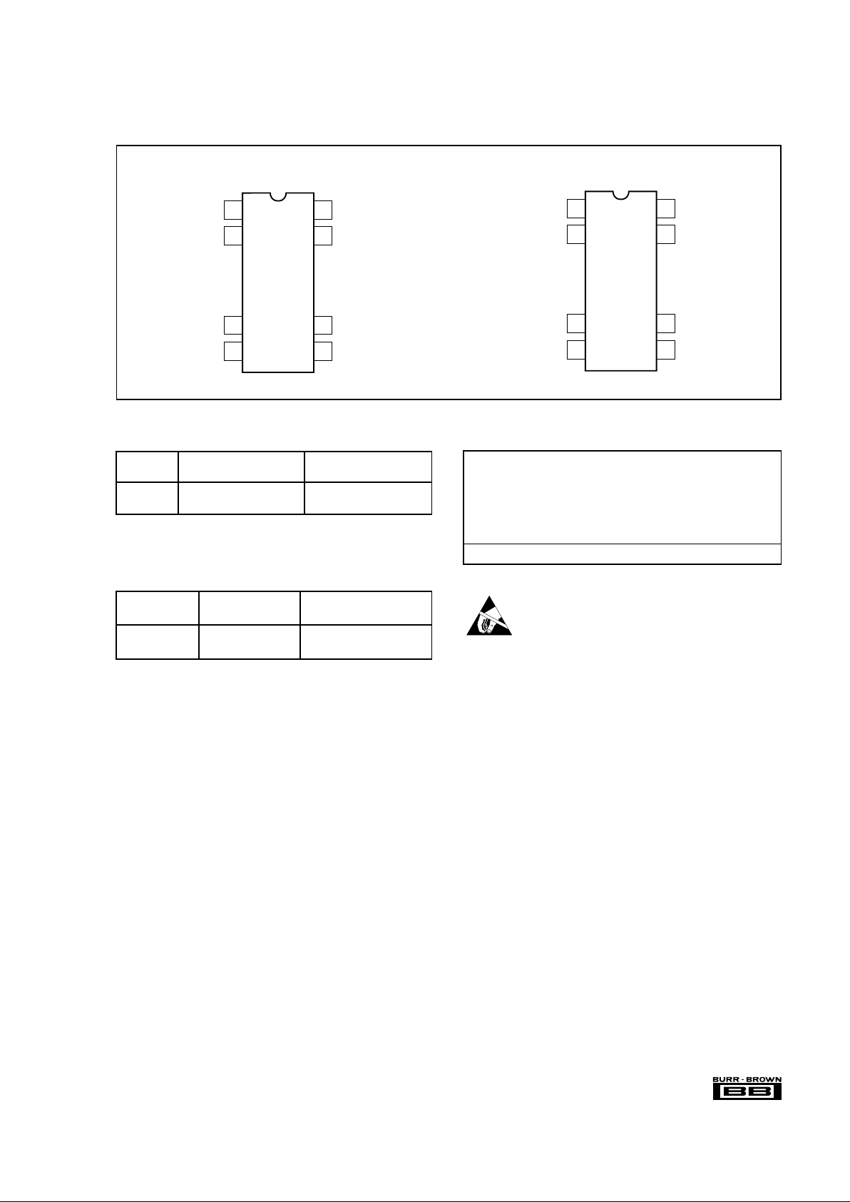
®
ISO124
1
2
28
27
16
15
13
14
+V
S1
–V
S1
V
OUT
Gnd
Gnd
V
IN
–V
S2
+V
S2
Top View —P Package Top View—U Package
CONNECTION DIAGRAM
ABSOLUTE MAXIMUM RATINGS
(1)
Supply Voltage................................................................................... ±18V
V
IN
......................................................................................................±100V
Continuous Isolation Voltage ..................................................... 1500Vrms
Junction Temperature .................................................................... +150°C
Storage Temperature....................................................................... +85°C
Lead Temperature (soldering, 10s)................................................ +300°C
Output Short to Common ......................................................... Continuous
NOTE: (1) Stresses above these ratings may cause permanent damage.
PACKAGE INFORMATION
PACKAGE DRAWING
PRODUCT PACKAGE NUMBER
(1)
ISO124P 16-Pin Plastic DIP 238
ISO124U 28-Lead Plastic SOIC 217-1
NOTE: (1) For detailed drawing and dimension table, please see end of data
sheet, or Appendix C of Burr-Brown IC Data Book.
1
2
16
15
10
9
7
8
+V
S1
–V
S1
V
OUT
Gnd
Gnd
V
IN
–V
S2
+V
S2
ELECTROSTATIC
DISCHARGE SENSITIVITY
This integrated circuit can be damaged by ESD. Burr-Brown
recommends that all integrated circuits be handled with
appropriate precautions. Failure to observe proper handling
and installation procedures can cause damage.
ESD damage can range from subtle performance degradation to complete device failure. Precision integrated circuits
may be more susceptible to damage because very small
parametric changes could cause the device not to meet its
published specifications.
NONLINEARITY
PRODUCT PACKAGE MAX %FSR
ISO124P 16-Pin Plastic DIP ±0.010
ISO124U 28-Lead Plastic SOIC ±0.010
ORDERING INFORMATION
4
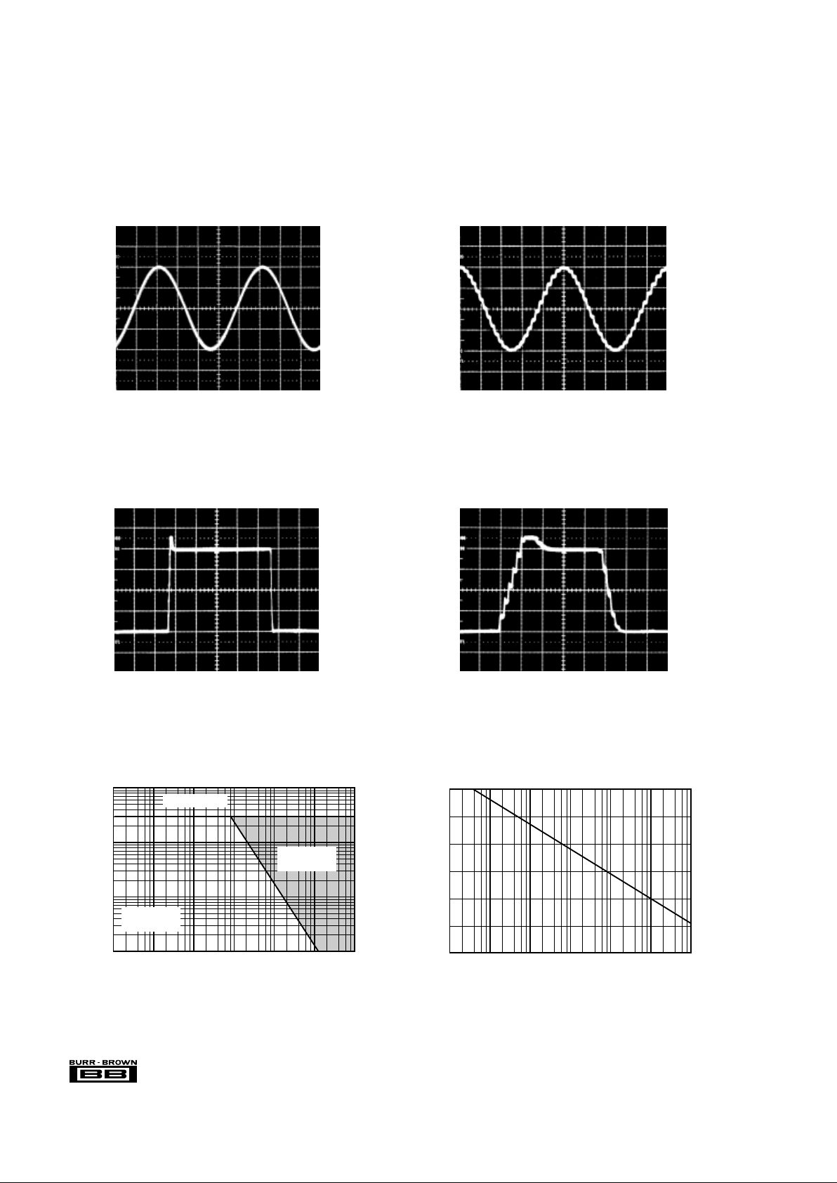
®
ISO124
Time (µs)
Time (µs)
+10
0
–10
0
STEP RESPONSE
500 1000
TYPICAL PERFORMANCE CURVES
At TA = +25°C, and VS = ±15V, unless otherwise noted.
+10
0
–10
0
SINE RESPONSE
(f = 2kHz)
Output Voltage (V)
Output Voltage (V)
SINE RESPONSE
(f = 20kHz)
Time (µs)
+10
0
–10
0
100
50
Output Voltage (V)
Time (µs)
+10
0
–10
0
STEP RESPONSE
100
50
Output Voltage (V)
1000500
ISOLATION VOLTAGE
vs FREQUENCY
Frequency (Hz)
Peak Isolation Voltage
100 1k 10k 100k 1M 10M 100M
1k
100
0
2.1k
Degraded
Performance
Typical
Performance
Max DC Rating
IMR vs FREQUENCY
Frequency (Hz)
IMR (dB)
160
140
120
100
80
60
40
1 10 100 1k 10k 100k 1M

5
®
ISO124
TYPICAL PERFORMANCE CURVES (CONT)
At TA = +25°C, and VS = ±15V, unless otherwise noted.
60
40
20
0
54
1 10 100 1k 10k 100k 1M
PSRR vs FREQUENCY
Frequency (Hz)
PSRR (dB)
–VS1, –V
S2
+VS1, +V
S2
100mA
10mA
1mA
100µA
10µA
1µA
0.1µA
1 10 100 1k 10k 100k 1M
ISOLATION LEAKAGE CURRENT vs FREQUENCY
Frequency (Hz)
Leakage Current (rms)
1500Vrms
240Vrms
0
–10
–20
–30
–40
250
200
150
100
50
0 500k 1M 1.5M
SIGNAL RESPONSE TO
INPUTS GREATER THAN 250kHz
Input Frequency (Hz)
V
OUT
/V
IN
(dBm)
Frequency Out
(NOTE: Shaded area shows aliasing frequencies that
cannot be removed by a low-pass filter at the output.)
V
OUT/VIN
100kHz
Frequency
Out

6
®
ISO124
THEORY OF OPERATION
The ISO124 isolation amplifier uses an input and an output
section galvanically isolated by matched 1pF isolating capacitors built into the plastic package. The input is dutycycle modulated and transmitted digitally across the barrier.
The output section receives the modulated signal, converts it
back to an analog voltage and removes the ripple component
inherent in the demodulation. Input and output sections are
fabricated, then laser trimmed for exceptional circuitry matching common to both input and output sections. The sections
are then mounted on opposite ends of the package with the
isolating capacitors mounted between the two sections. The
transistor count of the ISO124 is 250 transistors.
MODULATOR
An input amplifier (A1, Figure 1) integrates the difference
between the input current (V
IN
/200kΩ) and a switched
±100µA current source. This current source is implemented
by a switchable 200µA source and a fixed 100µA current
sink. To understand the basic operation of the modulator,
assume that VIN = 0.0V. The integrator will ramp in one
direction until the comparator threshold is exceeded. The
comparator and sense amp will force the current source to
switch; the resultant signal is a triangular waveform with a
50% duty cycle. The internal oscillator forces the current
source to switch at 500kHz. The resultant capacitor drive is
a complementary duty-cycle modulation square wave.
DEMODULATOR
The sense amplifier detects the signal transitions across the
capacitive barrier and drives a switched current source into
integrator A2. The output stage balances the duty-cycle
FIGURE 1. Block Diagram.
modulated current against the feedback current through the
200kΩ feedback resistor, resulting in an average value at the
V
OUT
pin equal to VIN. The sample and hold amplifiers in the
output feedback loop serve to remove undesired ripple
voltages inherent in the demodulation process.
BASIC OPERATION
SIGNAL AND SUPPLY CONNECTIONS
Each power supply pin should be bypassed with 1µF tantalum
capacitors located as close to the amplifier as possible. The
internal frequency of the modulator/demodulator is set at
500kHz by an internal oscillator. Therefore, if it is desired to
minimize any feedthrough noise (beat frequencies) from a
DC/DC converter, use a π filter on the supplies (see Figure 4).
ISO124 output has a 500kHz ripple of 20mV, which can be
removed with a simple two pole low-pass filter with a
100kHz cutoff using a low cost op amp (see Figure 4).
The input to the modulator is a current (set by the 200kΩ
integrator input resistor) that makes it possible to have an
input voltage greater than the input supplies, as long as the
output supply is at least ±15V. It is therefore possible when
using an unregulated DC/DC converter to minimize PSR
related output errors with ±5V voltage regulators on the
isolated side and still get the full ±10V input and output
swing. An example of this application is shown in Figure 9.
CARRIER FREQUENCY CONSIDERATIONS
The ISO124 amplifier transmits the signal across the isolation barrier by a 500kHz duty cycle modulation technique.
For input signals having frequencies below 250kHz, this
system works like any linear amplifier. But for frequencies
200kΩ
1pF
1pF
1pF
1pF
150pF
Osc
200µA
100µA
Sense
200µA
100µA
200kΩ
150pF
S/H
G = 1
S/H
G = 6
Sense
A2
A1
+V
S2
Gnd 2 –V
S2
+V
S1
Gnd 1 –V
S1
V
IN
V
OUT
Isolation Barrier

7
®
ISO124
1
2
7
9
10
8
PGA102
ISO124
ISO150
1
2
3
16
4
6
7
8
5
15 15
+15V –15V +15V –15V
V
IN
V
OUT
A
0
A
1
above 250kHz, the behavior is similar to that of a sampling
amplifier. The signal response to inputs greater than 250kHz
performance curve shows this behavior graphically; at input
frequencies above 250kHz the device generates an output
signal component of reduced magnitude at a frequency
below 250kHz. This is the aliasing effect of sampling at
frequencies less than 2 times the signal frequency (the
Nyquist frequency). Note that at the carrier frequency and its
harmonics, both the frequency and amplitude of the aliasing
go to zero.
ISOLATION MODE VOLTAGE INDUCED ERRORS
IMV can induce errors at the output as indicated by the plots of
IMV vs Frequency. It should be noted that if the IMV frequency
exceeds 250kHz, the output also will display spurious outputs
(aliasing) in a manner similar to that for V
IN
>250kHz and the
amplifier response will be identical to that shown in the “Signal
Response to Inputs Greater Than 250kHz” typical performance
curve. This occurs because IMV-induced errors behave like inputreferred error signals. To predict the total error, divide the isolation
voltage by the IMR shown in the “IMR versus Frequency” typical
performance curve and compute the amplifier response to this
input-referred error signal from the data given in the “Signal
Response to Inputs Greater Than 250kHz” typical performance
curve. For example, if a 800kHz 1000Vrms IMR is present, then
a total of [(–60dB) + (–30dB)] x (1000V) = 32mV error signal at
200kHz plus a 1V, 800kHz error signal will be present at the
output.
HIGH IMV dV/dt ERRORS
As the IMV frequency increases and the dV/dt exceeds
1000V/µs, the sense amp may start to false trigger, and the
output will display spurious errors. The common-mode
current being sent across the barrier by the high slew rate is
the cause of the false triggering of the sense amplifier.
Lowering the power supply voltages below ±15V may
decrease the dV/dt to 500V/µs for typical performance.
HIGH VOLTAGE TESTING
Burr-Brown Corporation has adopted a partial discharge test
criterion that conforms to the German VDE0884 Optocoupler Standards. This method requires the measurement of
minute current pulses (<5pC) while applying 2400Vrms,
60Hz high voltage stress across every ISO124 isolation
barrier. No partial discharge may be initiated to pass
this test. This criterion confirms transient overvoltage
(1.6 x 1500Vrms) protection without damage to the ISO124.
Lifetest results verify the absence of failure under continuous rated voltage and maximum temperature.
This new test method represents the “state-of-the art” for
non-destructive high voltage reliability testing. It is based on
the effects of non-uniform fields that exist in heterogeneous
dielectric material during barrier degradation. In the case of
void non-uniformities, electric field stress begins to ionize
the void region before bridging the entire high voltage
barrier. The transient conduction of charge during and after
the ionization can be detected externally as a burst of 0.01-
0.1µs current pulses that repeat on each ac voltage cycle.
The minimum ac barrier voltage that initiates partial discharge is defined as the “inception voltage.” Decreasing the
barrier voltage to a lower level is required before partial
discharge ceases and is defined as the “extinction voltage.”
We have characterized and developed the package insulation
processes to yield an inception voltage in excess of 2400Vrms
so that transient overvoltages below this level will not
damage the ISO124. The extinction voltage is above
1500Vrms so that even overvoltage induced partial discharge will cease once the barrier voltage is reduced to the
1500Vrms (rated) level. Older high voltage test methods
relied on applying a large enough overvoltage (above rating)
to break down marginal parts, but not so high as to damage
good ones. Our new partial discharge testing gives us more
confidence in barrier reliability than breakdown/no breakdown criteria.
FIGURE 3. Programmable-Gain Isolation Channel with
Gains of 1, 10, and 100.
FIGURE 2. Basic Signal and Power Connections.
+V
S1
+V
S2
Gnd
Gnd
V
IN
V
OUT
–V
S1
±V
S1
±V
S2
–V
S2
1µF 1µF
1µF
1µF
Isolation Barrier
ISO124

8
®
ISO124
FIGURE 5. Battery Monitor for a 600V Battery Power System. (Derives input power from the battery.)
FIGURE 4. Optional π Filter to Minimize Power Supply Feedthrough Noise; Output Filter to Remove 500kHz Carrier Ripple.
For more information concerning output filter refer to AB-023 and AB-034.
V
IN
V
OUT
= V
IN
Isolation Barrier
ISO124
+V
S2
+V
S1
–V
S1
±V
S1
–V
S2
Gnd2
Gnd1
R1
4.75kΩ
R2
9.76kΩ
1µF 1µF
1µF 1µF
10µH
10µH
±V
S2
10µH
10µH
1µF 1µF 1µF 1µF
C1
220pF
C2
1000pF
OPA237
15
1
9
10
7
2
e
50
= 12V
8
–V
16
+V
15
1
9
10
7
2
10kΩ
8
–V
16
+V
10kΩ
e
49
= 12V
e
2
= 12V
e
1
= 12V
10kΩ
10kΩ
Charge/Discharge Control
INA105
25kΩ
25kΩ
25kΩ
25kΩ
2
3
1
e
50
V =
2
+V –V
74
5
6
e
1
V =
2
Multiplexer
Control
Section
ISO124
This Section Repeated 49 Times.
ISO124

9
®
ISO124
FIGURE 6. Thermocouple Amplifier with Ground Loop Elimination, Cold Junction Compensation, and Up-scale Burn-out.
FIGURE 7. Isolated 4-20mA Instrument Loop. (RTD shown.)
R
CM
1kΩ
RCV420
XTR105
R
G
R
Z
(1)
13
3
4
2
6
7
10
14
1
0.01µF
4-20mA
RTD
(PT100)
0.8mA 0.8mA
1.6mA
14
15
16
3
2
10
4
12
11
5, 13
15
16
2
1
Gnd
–V
S
= –15V
on PWS740
+VS = 15V on PWS740
9
10
7
8
–V
+V
ISO124
V
OUT
0V - 5V
NOTE: (1) RZ = RTD resistance at minimum measured temperature.
2
6
10.0V
4
REF102
INA114
or
INA128
+In
7
4
3
8
1
2
5
16
15
8
10
ISO124
7
V
OUT
9
6
–In
+15V
+15V
–15V
+15V –15V
ISA
TYPE
E
J
K
T
MATERIAL
Chromel
Constantan
Iron
Constantan
Chromel
Alumel
Copper
Constantan
SEEBACK
COEFFICIENT
(µV/°C)
58.5
50.2
39.4
38.0
R
2
(R
3
= 100Ω)
3.48kΩ
4.12kΩ
5.23kΩ
5.49kΩ
R
4
(R
5
+ R6 = 100Ω)
56.2kΩ
64.9kΩ
80.6kΩ
84.5kΩ
+15V –15V
R3
100Ω
Ground Loop Through Conduit
NOTE: (1) –2.1mV/°C at 2.00µA.
R
1
27kΩ
Isothermal
Block with
1N4148
(1)
R
2
1MΩ
R
5
50Ω
R
G
R
4
R
6
100
Zero Adj
Thermocouple
2
1

10
®
ISO124
FIGURE 8. Isolated Power Line Monitor.
15
V–
V+
10
7
9
8
ISO124
1
2
16
15
16
V–
V+
10
7
9
8
ISO124
1
2
0.47µF
0.47µF
0.47µF
0.47µF
0.47µF
0.47µF
R
S
R
D1
I
L
Load
R
D2
V
L
Y
X
XY
10
P
L
= V
2
(R
D1
+ R
D2
)
R
S
R
D2
(V
2
)
MPY634
I
L
=
V
1
10R
S
(V
1
)
10kΩ2kΩ
2kΩ
0.01µF
V
L
= V
3
(R
D1
+ R
D2
)
R
D2
(V
3
)
OPA237
6
2
3
12
DCP011515
5 6 7
12
DCP011515
5 6 7

11
®
ISO124
FIGURE 10. Single Supply Operation of the ISO124 Isolation Amplifier. For additional information refer to AB-009.
R
1
R
2
R
4
INA105
Difference Amp
R
3
R
S
2
3
4
IN4689
5.1V
Reference
5
7
6
1
V
IN
Signal Source
+
NOTE: (1) Select to match R .
NOTE: Since the amplifier is unity gain, the input
range is also the output range. The output can go
to –2V since the output section of the ISO amp
operates from dual supplies.
S
10kΩ
15
–V
S2
(–15V)
+V
S2
(+15V)
V
S1
(+15V)
16
–V
S1
Com 2
10
In
Gnd
R
C
(1)
VS
(V)
20+
15
12
INPUT RANGE
(V)
(1)
–2 to +10
–2 to +5
–2 to +2
7
9
8
ISO124
2
1
V
OUT
= V
IN
FIGURE 9. Improved PSR Using External Regulator.
NOTE: The input supplies can be subregulated to ±5V to reduce
PSR related errors without reducing the ±10V input range.
10
7
9
8
2
V
OUT
+15V
–15V
VIN, up to
±10V Swing
+5V
Regulator
MC78L05
–5V
Regulator
MC79L05
0.47µF 0.47µF
0.1µF
1
2
3
0.1µF
0.47µF
ISO124
3
1
2
16
1
DCP011515
7
6 5 21

12
®
ISO124
FIGURE 12. Powered ISO Amp with Three-Port Isolation.
FIGURE 11. Input-Side Powered ISO Amp.
16
Gnd V
IN
V– V+
V+ V– V
O
Gnd
15
12
12
10 9
78
DCP011515
INPUT
SECTION
OUTPUT
SECTION
5 6 7
V
IN
Input
Gnd
+15V
–15V
–15V, 20mA
+15V, 20mA
Auxiliary
Isolated
Power
Output
Output
Gnd
V
O
ISO124
0.47µF
0.47µF
0.47µF
16
Gnd V
IN
V– V+
V+ V– V
O
Gnd
15
12
12
10 9
78
DCP011515
INPUT
SECTION
OUTPUT
SECTION
5 6 7
+15V Gnd
DCP011515
7
6 5 21
V
IN
Input
Gnd
+15V, 20mA
–15V, 20mA
–15V, 20mA
+15V, 20mA
Auxiliary
Isolated
Power
Output
Auxiliary
Isolated
Power
Output
Output
Gnd
V
O
ISO124
0.47µF
0.47µF
0.47µF
0.47µF
0.47µF
 Loading...