

Page 1
HT1611C
Timer with Dialer Interface
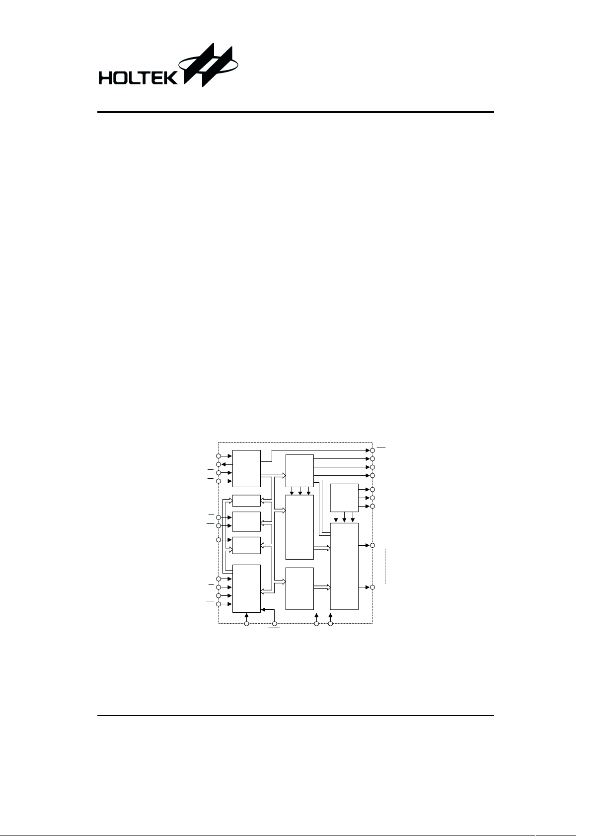
Block Diagram
Rev. 1.10 1 August 17, 2001
General Description
The HT1611C is a CMOS chip designed for dialer inter
faces driving 8 or 10-digit LCDs. Various functions, such
as real time clock, dialing number and conversation time
display are provided.
The real time is displayed by default. When answering a
telephone call, the timer is activated to tell users how
long the conversation has taken. After the telephone is
hung up, the total conversation time is shown for about 5
seconds and then the real time is displayed again.
When making a phone call, the HT1611C receives the
dialing data from the dialer and displays the phone num
ber from left to right on the LCD. However, if there is no
dialing action within 10 seconds, it restarts the timer
again. By adding a TIMER key, the HT1611C can provide a stopwatch function and timer reset/hold functions
(for details, refer to the functional description).
Features
·
Operating voltage: 1.2V~1.7V
·
Low operating current: 3mA (typ.)
·
Dialing number and conversation time display
·
Conversation timer (59 mins and 59 secs max.)
·
8 or 10-digit LCD display driver; 3V,1/2 bias, 1/3 duty
(8-digit hand-held calculator LCD used for 8-digit ap
-
plications)
·
Real time clock with stopwatch
·
Built-in dialer interface
·
12-hour or 24-hour format
·
Two-button sequential operation for real time clock
setting
·
Uses 32768Hz crystal
Applications
·
Timers, clocks, watches
·
LCD display drivers
·
Telephone display interface
·
Instrument display
Patent Number: 84545 (R.O.C.)
Patent Pending: 08/214, 079 (U.S.A.)
EPN
T1
T2
SEG1
SEG30
TIM ER
S1
HK
Tim e
Base
Tim er
Shift
R egister
State
C ontrol
C ontrol
Circuit
Comm on
Circuit
D ecoder
&
MUX
Voltage
D oubler
Segm ent
Latch
&
Select
Scan
CKT
X1
X2
S2
IN T
COM 1
COM 2
COM 3
VA
VB
VC
RT
12/24
VDD VSS
DI
SK
Page 2
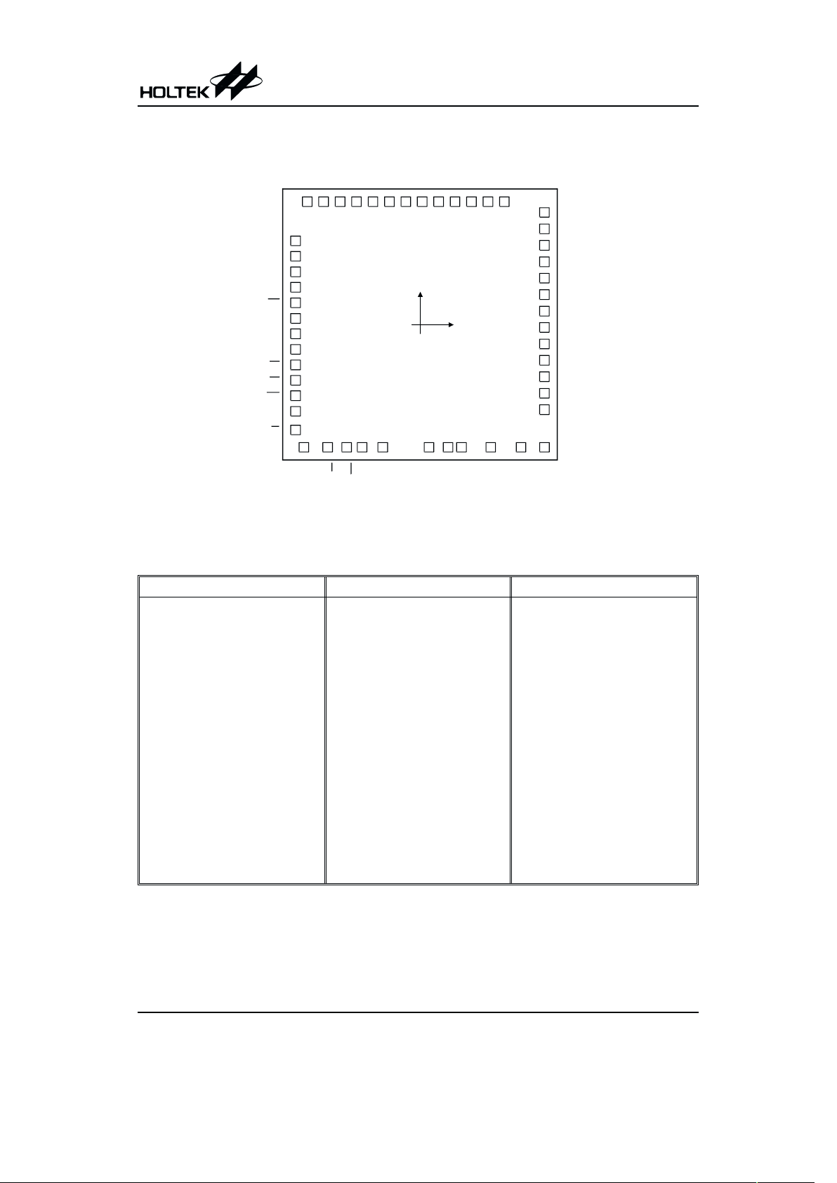
Pad Assignment
Chip size: 122.5 ´ 124.9 (mil)
2
* The IC substrate should be connected to VDD in the PCB layout artwork.
Pad Coordinates Unit: mil
Pad No. X Y Pad No. X Y Pad No. X Y
1
-55.73
37.50 18
-16.79 -54.72
35 55.46 35.51
2
-55.73
30.58 19 3.90
-54.72
36 55.46 42.86
3
-55.73
23.66 20 12.43
-54.72
37 55.46 50.20
4
-55.73
16.77 21 18.40
-54.72
38 37.60 55.02
5
-55.73
9.85 22 31.48
-54.72
39 30.26 55.02
6
-55.73
2.85 23 45.02
-54.72
40 22.91 55.02
7
-55.73 -4.07
24 55.50
-54.72
41 15.57 55.02
8
-55.73 -11.00
25 55.46
-37.96
42 8.22 55.02
9
-55.73 -17.96
26 55.46
-30.58
43 0.88 55.02
10
-55.73 -24.84
27 55.46
-23.24
44
-6.46
55.02
11
-55.73 -31.73
28 55.46
-15.89
45
-13.81
55.02
12
-55.73 -38.65
29 55.46
-8.55
46
-21.15
55.02
13
-55.73 -47.03
30 55.46
-1.21
47
-28.50
55.02
14
-52.02 -54.72
31 55.46 6.14 48
-35.84
55.02
15
-41.35 -54.72
32 55.46 13.48 49
-43.18
55.02
16
-32.86 -54.72
33 55.46 20.83 50
-50.53
55.02
17
-25.97 -54.72
34 55.46 28.17
HT1611C
Rev. 1.10 2 August 17, 2001
1
26
2
27
3
28
4
29
5
30
6
31
7
32
8
33
9
34
10
35
11
36
12
37
13
381439
15401641174218
43194420452146224723482449
25
50
(0,0)
DI
S1
VSS
VA
VB
VC
VDD
COM1
COM3
SEG1
SEG2
SK
SEG14
SEG13
SEG12
SEG11
SEG10
SEG9
SEG8
SEG7
SEG6
SEG5
SEG4
SEG3
SEG15
SEG16
SEG17
SEG18
SEG19
SEG20
SEG21
SEG22
SEG23
SEG24
SEG25
SEG26
SEG27
HK
INT
12/24
SEG28
SEG29
SEG30
COM2
S2
X2
X1
TIMER
T2
T1
Page 3
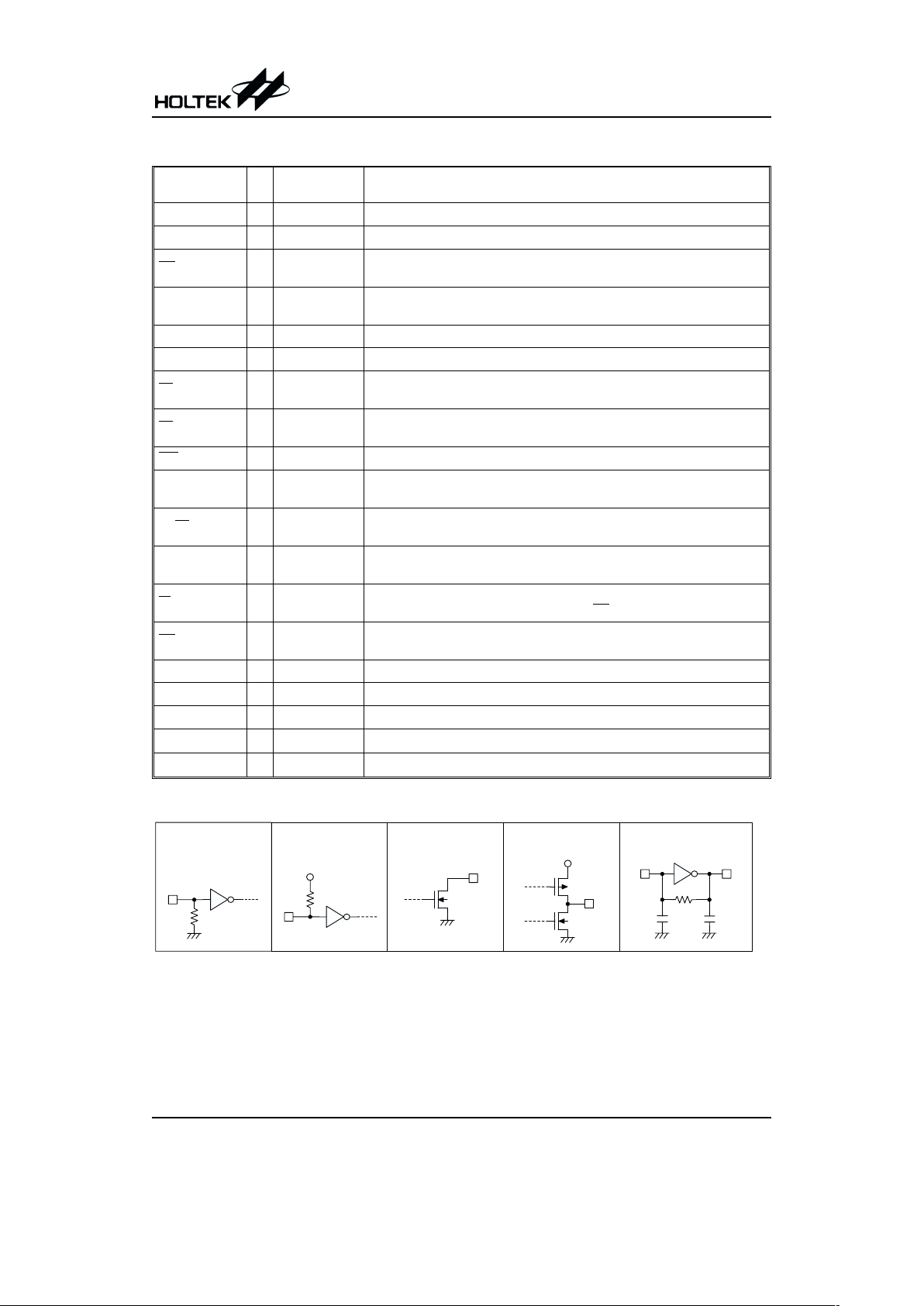
Pad Description
Pad Name I/O
Internal
Connection
Description
SEG1~SEG30 O CMOS OUT LCD segment signal output pads
COM1~COM3 O CMOS OUT LCD common signal output pads
HK
I
CMOS IN
Pull-high
Hook switch detector input
Active low
S2 I
CMOS IN
Pull-low
Clock adjusting switch
Active high
X2 O OSCILLATOR 32768Hz crystal oscillator output
X1 I OSCILLATOR 32768Hz crystal oscillator input
T2
I
CMOS IN
Pull-high
Test pad (connected to VSS for production test)
T1
I
CMOS IN
Pull-high
Test pad (connected to VSS for production test)
INT O NMOS OUT Interrupt output, 2Hz (default) or 16Hz (by mask option)
TIMER I
CMOS IN
Pull-low
Timer reset and start/hold toggle control input pad
12/24
I
CMOS IN
Pull-low
12-hour or24-hour format option pad, connectedto VDD for 12-hour format
S1 I
CMOS IN
Pull-low
Clock setting switch
Active high
DI
I
CMOS IN
Pull-high
Serial data input pad (connected to the dialer)
Data should be valid at the falling edge of SK
SK I
CMOS IN
Pull-high
Clock input pad (connected to the dialer)
VA O CMOS OUT Voltage doubler, connected to the external capacitor
VB O CMOS OUT Voltage doubler, connected to the external capacitor
VC O CMOS OUT Voltage doubler, connected to the external capacitor
VDD
¾¾
Positive power supply
VSS
¾¾
Negative power supply, ground
Approximate internal connection circuit
HT1611C
Rev. 1.10 3 August 17, 2001
NMOS OUTCMOS IN
Pull-low
CMOS IN
Pull-high
OSCILLATORCMOS OUT
X1
X2
12pF
15pF
10M
W
V
DD
V
DD
Page 4
Absolute Maximum Ratings
Supply Voltage ...........................................-0.3V to 5V
Storage Temperature .......................... -50°Cto125°C
Input Voltage ................................. V
SS
-0.3 to VDD+0.3
Operating Temperature ......................... -20°Cto75°C
Note: These are stress ratings only. Stresses exceeding the range specified under ²Absolute Maximum Ratings² may
cause substantial damage to the device. Functional operation of this device at other conditions beyond those
listed in the specification is not implied and prolonged exposure to extreme conditions may affect device reliabil
-
ity.
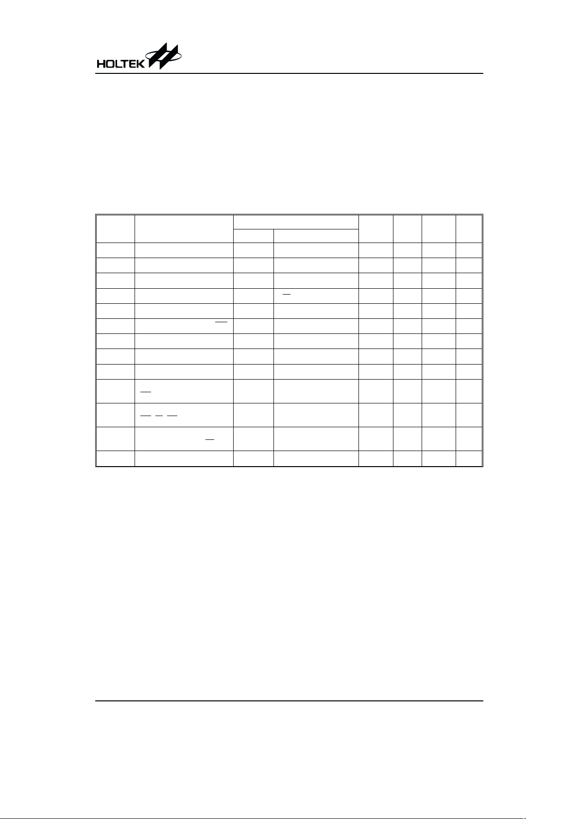
Electrical Characteristics
f
OSC
=32768Hz, Ta=25°C
Symbol Parameter
Test Conditions
Min. Typ. Max. Unit
V
DD
Conditions
V
DD
Operating Voltage
¾¾
1.2 1.5 1.7 V
V
IL
Input Low Voltage 1.2V~1.7V
¾
V
SS
¾
0.2V
DD
V
V
IH
Input High Voltage 1.2V~1.7V
¾
0.8V
DD
¾
V
DD
V
I
STB
Standby Current 1.5V
V
HK
=Floating (or VDD)
¾
0.1 1
mA
I
DD
Operating Current 1.5V No load
¾
310
mA
I
OL
Output Sink Current of INT 1.5V
V
O
=0.3V
500 1000
¾mA
t
A
Data Setup Time 1.5V
¾
1
¾¾ms
t
B
Data Hold On Time 1.5V
¾
2
¾¾ms
t
C
Inter Digit Time 1.5V
¾
5
¾¾ms
t
DB
Debounce Time
(HK
, S1, S2, TIMER)
1.5V
¾¾
31.25
¾
ms
R
HI
Pull-high Resistance
(HK
,DI,SK)
1.5V
V
IN
=0V
¾
1
¾ MW
R
LO
Pull-low Resistance
(TIMER, S1, S2, 12/24
)
1.5V
V
TIMER
=1.5V
¾
5
¾ MW
f
OSC
System Frequency 1.5V Crystal=32768Hz
¾
32768
¾
Hz
HT1611C
Rev. 1.10 4 August 17, 2001
Page 5

Functional Description
Operational flow chart
HT1611C
Rev. 1.10 5 August 17, 2001
HK=0 ?
"HK= 1"
> 5 secs ?
HK= "0" ?
N
N
N
Y
Y
N
N
Y
Y
N
Y
Y
Reset to 00 00
start real time clock
Display real time
Trig.
TIMER key?
N
Display dialing number
Timer stops, displays
total conversation time
Over 5 secs ?
N
Y
Y
N
Y
N
Y
Y
Reset to 00 00
& start timer
Keep counting
Timer hold
> 5 secs ?
N
Y
N
Power-on
Timer keeps counting,
displays timer value
Reset to 00 00
& start timer
Dialing data input ?
Trig. TIME R key ?
HK= "0" ?
HK= "0" ?
N
Y
HK= "0" ?
No
data in > 10 s ?
Trig. TIME R key ?
Trig. TIME R key ?
Trig. TIME R key ?
N
N
Y
Y
Reset to 00 00
& start timer
Keep counting
Timer hold
Trig. TIME R key ?
Trig. TIME R key ?
HK= "0" ?
N
N
Y
Y
N
Y
N
Y
HK=1
>5sec?
Page 6

On-hook & off-hook
Note: Block A shows the switches S1 and S2 that are used for setting and selecting.
Block B illustrates a timer mode when Off-hook; timer resets and starts to count the conversation time.
In Block C, the dialing data is received and displayed on the LCD from left to right after Off-hook. When the entry interval is over 10 seconds, it resets the timer and starts to count.
TIMER key function
The TIMER key is used to start/stop the timer (toggle). In real time mode, it can perform a stopwatch function.
In the conversation timer mode, it can reset or hold the timer.
HT1611C
Rev. 1.10 6 August 17, 2001
Block A Block B
Block C
Receive Digit(s)
78
7
780
On-hook
Receive Data
No Data
Entry >10 secs
Timer Mode
On-hook
00 01
00 02
11
26
10 25 37
S2
S2
S2
S1
S1
Hour
Minute
Real Time
Display Timer
5 sec duration
> 5 secs
< 5 secs and
Off-hook
Off-hook
00 00
Trig. TIME R
(within 5 secs) Timer reset
and count
00 00
01 24
Trig.
TIMER
01 24
Timer hold
No action for
over 5 secs
Timer reset
and count
00 00
00 12
LCD display
real time
10 11 00
00 12 36
Return to real
time clock
00 12
Timer hold
Trig. TIME R Trig. TIME R
(HK=0)
Off-hook Dialing out
Timer reset
and count
00 00
01 24
Trig.
TIMER
Timer reset
and count
00 00
00 12
LCD display
real time
10 11 00 1234567
Dialing finished
(after 10 secs)
01 24
Timer hold
00 24 36
Return to real
time clock
On-hook
over 5 secs
Trig. TIME R
Timer reset
and count
00 00
01 24
Show dialing
numbers
Page 7

·
Data latch timing
HT1611C
Rev. 1.10 7 August 17, 2001
Data & Timing
·
For telephone application
The HT1611C is designed to display telephone num
-
bers derived from the HT93XXX series telephone dial
ers. The corresponding data is illustrated in the
following table.
·
For instrument or mC application
The HT1611C is also capable of displaying BCD data
generated from instrument or a mC system. The corre
sponding data and timing is shown in the Data latch
timing. Before the data is transmitted to the HT1611C,
the HK
pin should be pulled-low or continuously kept
low. The HT1611C is then ready to receive the data.
At the falling edge of the clock the data is shifted in to
the IC. After all the data is sent to the HT1611C, the
SK
pin isset low to avoid switchingto the timer mode.
K ey-In
Data Code
Display
b3
b2
b1
b0
Blank
1
2
3
4
5
6
7
8
9
0
*
#
F
P
1
0
0
0
0
0
0
0
0
1
1
1
1
1
1
11
1
0
1
1
0
0
0
1
1
1
1
0
0
0
0
00
01
110
1
0
1
0
1
0
1
0
1
0
1
0
1
1
1
1
0
0
1
0
0
1
1
0
0
Blank
DI
SK
Digit 1
Digit 2
Digit N
b3 b0b1b2 b3 b0b1b2 b0b1
t
A
t
B
t
C
Page 8

Application Circuits
For telephone interfacing (with batteries)
* The IC substrate should be connected to VDD in the PCB layout artwork.
HT1611C
Rev. 1.10 8 August 17, 2001
HDI
SKDI
PO
12/24
HK
0.1mF
TIM ER
32768H z
8 /1 0 -D ig it L C D
COM
SEG
COM
SEG
COM
30 2131
S1
S2
1.5V
H T1611C
1
26
2
27
3
28
4
29
5
30
6
31
7
32
8
33
9
34
10
35
11
36
12
37
13
38
14
39 40
16
41
17
42
18
43
19
44
20
45
21
46
22
47
23
48
24
49
25
50
15
DO CLOCK
47k
W
HT93XXX Dialer
HFO
8050
HFI
330mF
10V
VSS
47k
W
1A bridge
Ring
Tip
A92
33k
W
100k
W
100k
W
HFI VDD
8050
270k
W
47k
W
A42
2.7k
W
5.1V
220k
W
10M
W
330k
W
HKS
1N 4148´3
+
O ff-h o o k
On-hook
HDI
VSS
X1 X2
3.58M H z
0.1
m
F
0.02
m
F
Page 9

For telephone interfacing (without batteries)
* The IC substrate should be connected to VDD in the PCB layout artwork.
HT1611C
Rev. 1.10 9 August 17, 2001
HDI
SKDI
TIM ER
32768H z
8 /1 0 -D ig it L C D
COM
SEG
COM
SEG
COM
30 2131
H T1611C
1
26
2
27
3
28
4
29
5
30
6
31
7
32
8
33
9
34
10
35
11
36
12
37
13
38
14
39 40
16
41
17
42
18
43
19
44
20
45
21
46
22
47
23
48
24
49
25
50
15
DO CLOCK
47k
W
HT93XXX Dialer
HFO
8050
HDI
330mF
10V
VSS
47k
W
1A bridge
Ring
Tip
A92
33k
W
100k
W
100k
W
HFI VDD
8050
270k
W
47k
W
A42
2.7k
W
5.1V
220k
W
10M
W
330k
W
1N 4148´6
20k
W
1mF
HK
PO
HKS
O ff-hook
On-hook
VSS
X1 X2
3.58M H z
HFI
0.1mF
0.1
m
F
0.02
m
F
Page 10

For instrument or mC use
* The IC substrate should be connected to VDD in the PCB layout artwork.
Note:
To drive SK
, DI,HK, an open drain NMOS output structure is recommended.
To drive SK
,DIand HK with a CMOS output structure, a voltage divider is needed (R=4.3kW, R1=10kW).
HT1611C
Rev. 1.10 10 August 17, 2001
SK
TIM ER
32768H z
8 /1 0 -D ig it L C D
COM
SEG
COM
SEG
COM
30 2131
S1
S2
1.5V
H T1611C
1
26
2
27
3
28
4
29
5
30
6
31
7
32
8
33
9
34
10
35
11
36
12
37
13
38
14
39 40
16
41
17
42
18
43
19
44
20
45
21
46
22
47
23
48
24
49
25
50
15
DO CLOCK
VDD
5V
VSS
In s tru m e n t o r mC S ystem
R1
R
R1
R
R1
R
+
HK
12/24
DI
HK
0.1mF
0.1
m
F
Page 11

LCD Configuration
For 8-digit application
·
Segment electrode side
LCD driving system 1/2 bias, 1/3 duty, 3V
·
Common electrode side
·
LCD connection
HT1611C
Rev. 1.10 11 August 17, 2001
COM1COM3SEG7SEG8SEG9SEG10SEG11SEG12SEG13SEG14SEG15SEG16SEG17SEG18SEG19SEG20SEG21SEG22SEG23SEG24SEG25SEG26SEG27SEG28SEG29SEG30COM
2
789 27 28 29 3021 22 23 24 25 2615 16 17 18 19 2010 11 12 13 14SEG
COM1
COM2
COM3
Page 12

For 10-digit application
·
Segment electrode side
LCD driving system 1/2 bias, 1/3 duty, 3V
·
Common electrode side
·
LCD connection
HT1611C
Rev. 1.10 12 August 17, 2001
2
1178910
11 1 2
21
2019181716
151413
22 23 24 252627 28 30 2
4563
SEG
SEGCOM SEG SEG SEG SEG
SEG
SEG SEGSEG
SEGSEGSEGSEG
SEGSEGSEG
SEG SEG SEG SEG
SEG SEG
SEG SEG COM
SEG
29
SEG SEG SEG
SEG
COM
3
789 27 28 29 3021 22 23 24 25 2615 16 17 18 19 2010 11 12 13 14SEG 456123
COM1 CO
M
Page 13

HT1611C
Rev. 1.10 13 August 17, 2001
Copyright Ó 2001 by HOLTEK SEMICONDUCTOR INC.
The information appearing in this Data Sheet is believed to be accurate at the time of publication. However, Holtek as
sumes no responsibility arising from the use of the specifications described. The applications mentioned herein are used
solely for the purpose of illustration and Holtek makes no warranty or representation that such applications will be suitable
without further modification, nor recommends the use of its products for application that may present a risk to human life
due to malfunction or otherwise. Holtek¢s products are not authorized for use as critical components in life support devices
or systems. Holtek reserves the right to alter its products without prior notification. For the most up-to-date information,
please visit our web site at http://www.holtek.com.tw.
Holtek Semiconductor Inc. (Headquarters)
No.3, Creation Rd. II, Science Park, Hsinchu, Taiwan
Tel: 886-3-563-1999
Fax: 886-3-563-1189
http://www.holtek.com.tw
Holtek Semiconductor Inc. (Taipei Sales Office)
4F-2, No. 3-2, YuanQu St., Nankang Software Park, Taipei 115, Taiwan
Tel: 886-2-2655-7070
Fax: 886-2-2655-7373
Fax: 886-2-2655-7383 (International sales hotline)
Holtek Semiconductor Inc. (Shanghai Sales Office)
7th Floor, Building 2, No.889, Yi Shan Rd., Shanghai, China 200233
Tel: 021-6485-5560
Fax: 021-6485-0313
http://www.holtek.com.cn
Holtek Semiconductor Inc. (Shenzhen Sales Office)
5/F, Unit A, Productivity Building, Cross of Science M 3rd Road and Gaoxin M 2nd Road, Science Park, Nanshan District,
Shenzhen, China 518057
Tel: 0755-8616-9908, 8616-9308
Fax: 0755-8616-9533
Holtek Semiconductor Inc. (Beijing Sales Office)
Suite 1721, Jinyu Tower, A129 West Xuan Wu Men Street, Xicheng District, Beijing, China 100031
Tel: 010-6641-0030, 6641-7751, 6641-7752
Fax: 010-6641-0125
Holtek Semiconductor Inc. (Chengdu Sales Office)
709, Building 3, Champagne Plaza, No.97 Dongda Street, Chengdu, Sichuan, China 610016
Tel: 028-6653-6590
Fax: 028-6653-6591
Holmate Semiconductor, Inc. (North America Sales Office)
46729 Fremont Blvd., Fremont, CA 94538
Tel: 510-252-9880
Fax: 510-252-9885
http://www.holmate.com
 Loading...