

Page 1
Features
Operating voltage: 1.5V
·
Auto walking or jogging detection
·
Step number/mileage/kilometer/calorie
·
display
LCD display
·
General Description
The HT1350 is a step counter IC implemented
in the CMOS technology. It provides an LCD
with a whole course (kilometer/mile) as well as
the consumed calorie display.
The HT1350 consists of internal oscillator cir
cuit, a step number/kilometer/mile/calorie step
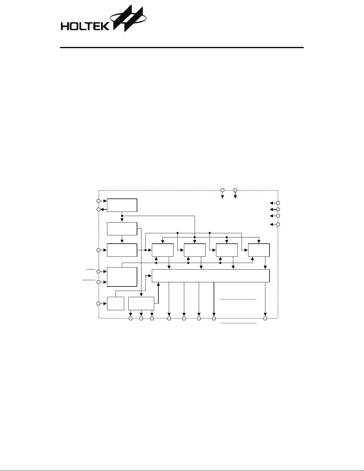
Block Diagram
HT1350
Step Counter
An oscillator with 32kHz
·
Few external components
·
Low power consumption
·
An LCD with 1/3 duty, 1/2 bias
·
counter, a voltage doubler, and an LCD display
multiplexer.
The IC can automatically distinguish walking
from jogging, thus making appropriate calcula
tions.
-
VDD VSS
-
OSC1
OSC2
STEP
WALK/RUN
AUTO /M AN U
MODE
O scillator
P re scaler
Step Pulse
G enerator
Auto-Detect
Circuit
(Jog/W alk)
M ode
Switch
Level Shift
Circuit
CP1 CP2 CP3 COM1 COM2 COM3 OUT4 OUT17
Step
C ounter
Mile
C ounter
M u lt ip le x e r C irc u it
1 June 28, 1999
Km
C ounter
TEST1
TEST2
TEST3
RESET
Cales
C ounter
Page 2
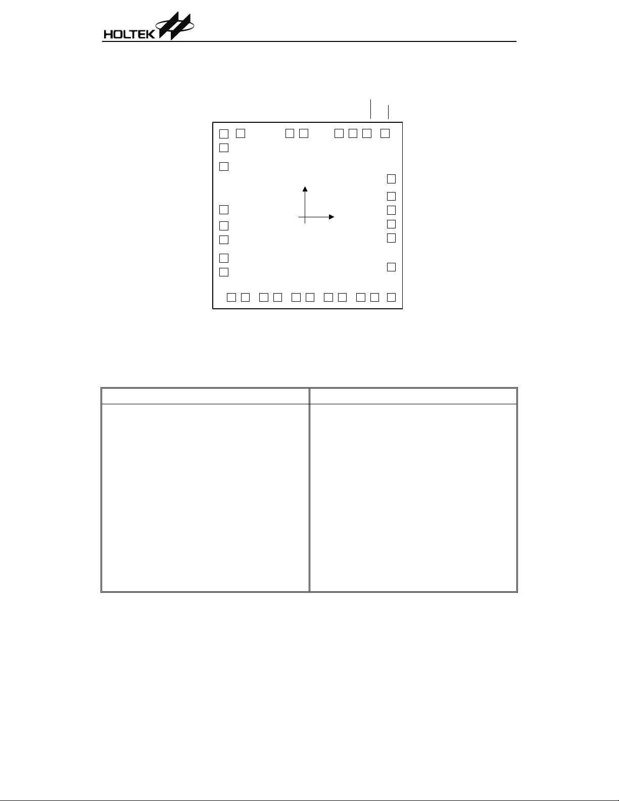
Pad Assignment
HT1350
AUTO /M AN U
WALK/RUN
RESET
MODE
VSS
TEST3
VDD
TEST2
TEST1
OSC2
OSC1
OUT17
OUT16
OUT15
OUT14
1
2
3
4
5
6
7
8
32
92510
OUT13
11
OUT12
OUT11
30
31
13
12
OUT9
OUT10
Chip size: 2725 ´ 2780 (mm)
(0,0)
14
OUT8
29
28
16
15
OUT7
OUT6
26
27
STEP
24
CP1
23
CP2
22
CP3
21
COM 1
20
COM 2
18
17
19
OUT5
OUT4
COM 3
2
* The IC substrate should be connected to VDD in the PCB layout artwork.
Pad No. X Y Pad No. X Y
1
2
3
4
5
6
7
8
9
10
11
12
13
-1206.00
-1206.00
-1206.00
-1206.00
-1206.00 -159.50
-1206.00 -359.50
-1206.00 -624.50
-1206.00 -824.50
-1098.00 -1190.50
-898.00 -1190.50
-633.00 -1190.50
-433.00 -1190.50
-168.00 -1190.50
14 32.00
15 297.00
16 497.00
1159.50 17 762.00
994.50 18 962.00
661.70 19 1202.00
71.50 20 1202.00
21 1202.00
22 1202.00
23 1202.00 65.50
24 1202.00 259.50
25 1202.00 537.00
26 1078.00 1167.50
27 812.00 1167.50
28 631.00 1167.50
29 447.00 1167.50
-1190.50
-1190.50
-1190.50
30
31
32
-59.00
-259.00
-966.00
-1190.50
-1190.50
-1190.50
-753.50
-335.50
-135.50
1167.50
1167.50
1167.50
Unit: mm
2 June 28, 1999
Page 3

Pad Description
HT1350
Pad No Pad Name I/O
1 TEST2 I/O
2 TEST1 I/O
3 OSC2 O
4 OSC1 I
Internal
Connection
¾
¾
¾
¾
Descriptions
For IC test only
For IC test only
Oscillator output
Oscillator input
5~18 OUT17~OUT4 O CMOS Display data output pads for segments
19~21 COM3~COM1 O NMOS Display data output pads for commons
22 CP3 O * Bias supply voltage pad for driving the LCD panel
23~24 CP2~CP1 O * LCD bias supply voltage control pads
I
CMOS
Pull-high
CMOS
Pull-high
CMOS
Pull-high
¾
¾
¾
CMOS
Pull-high
CMOS
Pull-high
Step sensor input pad
Walk/Run mode manual set pad
Auto detection/Manual set selection pad
Positive power supply
For IC test only
Negative power supply (GND)
LCD display mode selection
System reset pad
25 STEP I
26 WALK/RUN
27 AUTO/MANU I
28 VDD I
29 TEST3 I/O
30 VSS I
31 MODE O
32 RESET O
Approximate internal connection circuits
CMOS IN
Pull-high
VDD
CMOS OUT
(F o r C O M 1 ~ C O M 3 )
NMOS OUT
CP1
COM 1~
COM 3
VSS
3 June 28, 1999
CP3
CP2
OSCILLATORCP1~CP3
VDD VD D
OSC1
OSC2
Page 4

Absolute Maximum Ratings
HT1350
Supply Voltage.................................-0.3V to 5V
Input Voltage .................V
-0.3V to VDD+0.3V
SS
Storage Temperature.................-50°Cto125°C
Operating Temperature ..................0°Cto70°C
Note: These are stress ratings only. Stresses exceeding the range specified under ²Absolute Maxi
mum Ratings² may cause substantial damage to the device. Functional operation of this de
vice at other conditions beyond those listed in the specification is not implied and prolonged
exposure to extreme conditions may affect device reliability.
Electrical Characteristics
Ta=25°C
Test Conditions
Symbol Parameter
V
I
I
V
V
f
DD
DD
STB
IL
IH
OSC
Operating Voltage
Operating Current 1.5V
Standby Current 1.5V
Input Low Voltage 1.5V
Input High Voltage 1.5V
System Frequency 1.5V
DD
Conditions
V
¾¾
No load,
=32kHz
f
OSC
¾¾
¾¾¾
¾
¾¾32¾
Min. Typ. Max. Unit
1.3 1.5 1.7 V
¾
1.5 3
0.5 1
0.2V
DD
0.8V
¾¾
DD
kHz
mA
mA
V
V
Functional Description
The HT1350 is a step counter IC. It is used to automatically count the step number taken by a
runner and to display the whole course (kilometer/mile) combined with the calories consumed
on the LCD.
The IC is turned on and off with respect to the
on/off status of a short of spring switch which
corresponds to the up/down motion of the steps.
The output of step number can be changed to
kilometers/miles or calories by counting the to
tal number of times the step switch is closed.
The IC can automatically distinguish between
walking and jogging and make the according
calculations. The output of the LCD is busy
when the RESET key is pressed. Once the LCD
is in the busy state, the step counter will start
counting at 0 after 0.5 seconds till the runner
stops running and stands still. After the step
counter stops counting, pressing the MODE
key will display the step number®mile®kilo
meter®calorie in sequence.
-
-
-
-
4 June 28, 1999
Page 5

LCD Display
D ig it 5 D ig it 4 D ig it 3 D ig it 2 D ig it 1
a
HT1350
f
g
e
d
12345
12345
Com1
Com2
Application Circuit
Com3
b
c
D3c
D2e
D2f
D2a
P1
D2d
D2g
D2b
D1e
D1f
D1a
14 15 16
14 15 16
D1d
P1 P2
D1g
D2c
D1c
D1b
D4c
Cals
17
17
M ile s
D5c
Km
D5e
D5f
D5a
P2
6 7 8 9 10 11 12 13
6 7 8 9 10 11 12 13
D4d
D3e
D3f
D3a
D3d
D3g
D3b
D5d
D5g
D5b
D4e
D4f
D4a
D4g
D4b
102
1.5V
COM 1 CO M2
COM 3
OUT4 OUT17
CP3
VDD
VSS
OSC1 OSC2 RESET MODE
0 6 !#
32kHz
5 June 28, 1999
X 14
CP1
102
CP2
STEP
Page 6

HT1350
Holtek Semiconductor Inc. (Headquarters)
No.3 Creation Rd. II, Science-based Industrial Park, Hsinchu, Taiwan, R.O.C.
Tel: 886-3-563-1999
Fax: 886-3-563-1189
Holtek Semiconductor Inc. (Taipei Office)
5F, No.576, Sec.7 Chung Hsiao E. Rd., Taipei, Taiwan, R.O.C.
Tel: 886-2-2782-9635
Fax: 886-2-2782-9636
Fax: 886-2-2782-7128 (International sales hotline)
Holtek Microelectronics Enterprises Ltd.
RM.711, Tower 2, Cheung Sha Wan Plaza, 833 Cheung Sha Wan Rd., Kowloon, Hong Kong
Tel: 852-2-745-8288
Fax: 852-2-742-8657
Copyright 1999 by HOL TEK SEMICONDUCTOR INC.
The information appearing in this Data Sheet is believed to be accurate at the time of publication. However, Holtek
assumes no responsibility arisingfrom the use of the specifications described. The applications mentioned herein are
used solely for the purpose of illustration and Holtek makes no warranty or representation that such applications
will be suitable without further modification, nor recommends the use of its products for application that may pres
ent a risk to human life due to malfunction or otherwise. Holtek reserves the right to alter its products without prior
notification. For the most up-to-date information, please visit our web site at http://www.holtek.com.tw.
6 June 28, 1999
-
 Loading...