

Page 1
MICROWAVE CORPORATION
GaAs MMIC VOLTAGE VARIABLE ATTENUATOR 1.5 - 2.3 GHz
FEBRUARY 2001
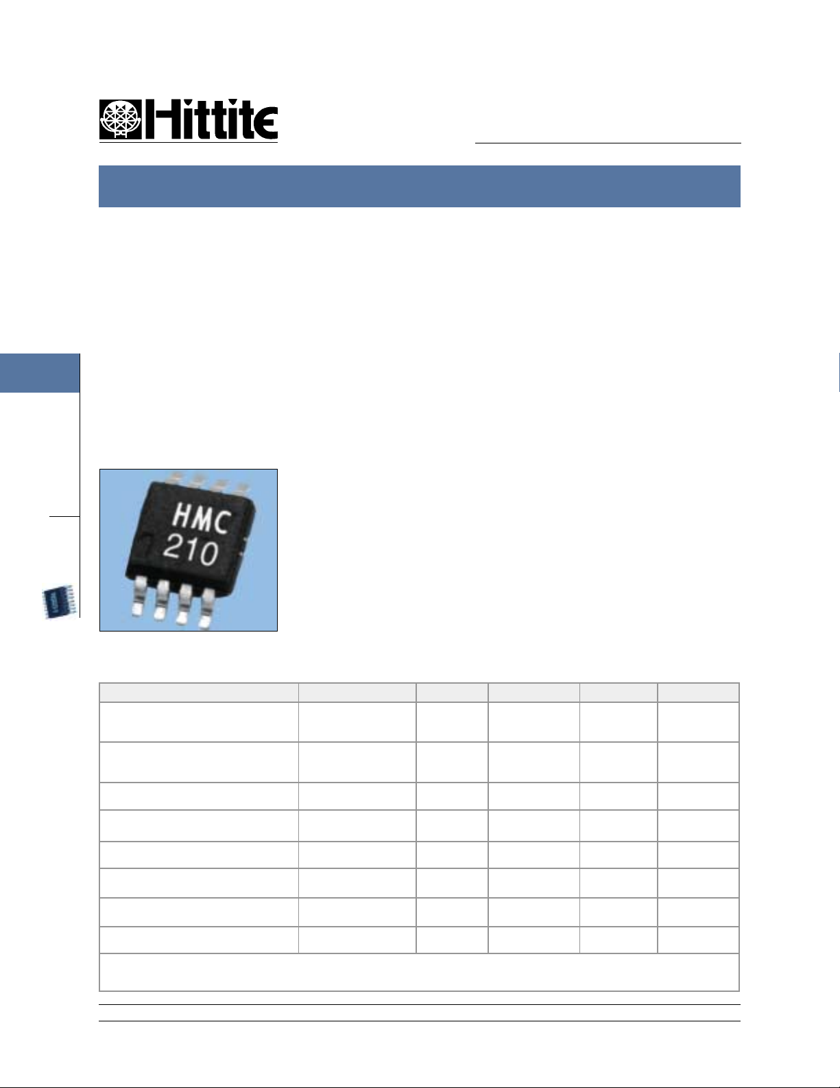
HMC210MS8
2
ATTENUATORS
SMT
Features
SINGLE POSITIVE VOLTAGE CONTROL: 0 to +2.5V
HIGH ATTENUATION RANGE: >50 dB @ 1.9 GHz
HIGH INPUT IP3: +15 dBm Typical
(All Attenuation States)
ULTRA SMALL PACKAGE: MSOP
General Description
The HMC210MS8 is a miniature absorptive voltage variable attenuator in an 8lead MSOP package. The device operates with a positive supply voltage (+2.5V),
and a positive control voltage. A unique
feature is the high third order intercept
point for all attenuation states. The
HMC210MS8 is ideal for operation in PCS
applications at 1.9 GHz and W-CDMA
applications through 2.2 GHz. Operation
up to 2.3 GHz is possible, with a reduced
attenuation range of 31 dB.
Guaranteed Performance V
= +2.5 Vdc, 50 Ohm System, -40 to +85°C
dd
Parameter Condition Min Typical Max Units
Insertion Loss
(Vctl = 0 V Min.Atten.)
Attenuation Range
(Vctl=0to+2.5V)
Return Loss
(Vctl=0to+2.5V)
Input Power for 0.1 dB
Compression (f = 1.9 GHz)
Input Power for 1.0 dB
Compression (f = 1.9 GHz))
Input Third Order Intercept
(f = 1.9 GHz, two tones @ +5dBm)
Rise / Fall Time (tRise /tFall)
Note 1
On Time (tOnTotal)
Note 2
Note 1:Ri se T ime(tRise) and Fall Time (tFall) are measured between the 10% and 90% attenuation values.
Note 2:The On Time (tOn Total)is defined as the time fromthe 50% control signal level point to the maximum attenuation
level.
12 Elizabeth Drive, Chelmsford, MA 01824 Phone: 978-250-3343 Fax: 978-250-3373 Web Site: www.hittite.com
1.8 - 2.0 GHz
1.7 - 2.1 GHz
1.5 - 2.3 GHz
1.8 - 2.0 GHz
1.7 - 2.1 GHz
1.5 - 2.3 GHz
1.5 - 2.0 GHz
2.0 - 2.3 GHz
Min.Atten.
Atten.>2.0 dB
Min.Atten.
Atten.>2.0 dB
Min.Atten.
Atten.>2.0 dB
1.5 - 2.3 GHz 0.9 uS
1.5 - 2.3 GHz 2.6 uS
44
39
31
17
0
30
10
3.3
3.4
3.0 - 5.0
55
43
40
9
6
15
-5
20
3
35
15
4.9
5.5
7.5
dB
dB
dB
dB
dB
dB
dB
dB
dBm
dBm
dBm
dBm
dBm
dBm
2 - 32
Page 2
HMC210MS8
MICROWAVE CORPORATION
HMC210MS8 VOLTAGE VARIABLE ATTENUATOR 1.5 - 2.3 GHz
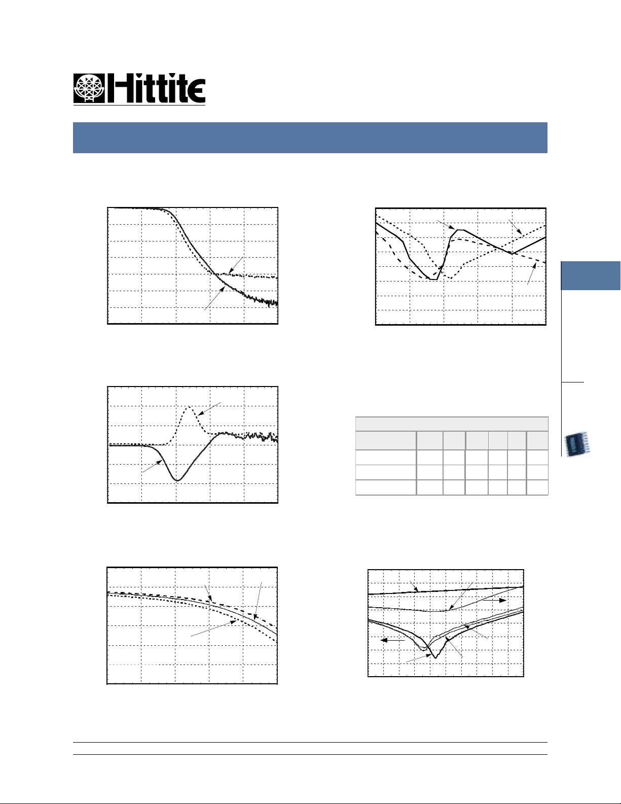
Relative Attenuation vs. Control
Voltage@1.9 and 2.2 GHz
0
-10
-20
-30
-40
-50
-60
RELATIVE ATTENUATION (dB)
-70
0 0.5 1 1.5 2 2.5
f= 1.9 GHz
CONTROL VOLTAGE (V)
f= 2.2GHz
Attenuation vs. Temperature
Normalized to +25°C @1.9 GHz
15
10
5
0
-5
+85 C
-10
NORMALIZED ATTENUATION (dB)
-15
0 0.5 1 1.5 2 2.5
CONTROL VOLTAGE (V)
-40 C
Broadband Insertion Loss
0
-2
-4
-6
-8
INSERTION LOSS (dB)
-10
-12
1.5 1.7 1.9 2.1 2.3 2.5
FREQUENCY (GHz)
-40 C
+85 C
+25 C
Input IP3 vs. Control Voltage
@1.9 GHz
40
35
30
25
20
15
INPUT IP3 (dBm)
10
5
0
0 0.5 1 1.5 2 2.5
+25 C
CONTROL VOLTAGE (V)
Typical Input P1dB Compression
@1.9 GHz vs. Temperature
Input Power For 1 dB Compression Point
Test Condition
(1.9 GHz)
Min. Attenuation 0.0 +2.5 20 20 21 dBm
Max.Attenuation +2.5 +2.5 19 16 25 dBm
WorstCase P1dB +1.0 +2.5 3 4 3 dBm
V
CTL
(Vdc)
Vdd
(Vdc)
Broadband Maximum Relative
Attenuation and Return Loss
0
Vctl = +2.5 V
+25 C
ATTEN.
1.5 1.7 1.9 2.1 2.3 2.5
FREQUENCY (GHz)
RELATIVE ATTENUATION (dB)
-10
-20
-30
-40
-50
-60
-70
-80
FEBRUARY 2001
-40 C
+85 C
+25C +85C -40C Units
Vctl = 0 V
+85 C ATTEN
-40 C
ATTEN.
0
-5
-10
-15
-20
-25
-30
-35
-40
2
ATTENUATORS
SMT
RETURN LOSS (dB)
S - Parameter data is available On-Line at www.hittite.com
12 Elizabeth Drive, Chelmsford, MA 01824 Phone: 978-250-3343 Fax: 978-250-3373 Web Site: www.hittite.com
2 - 33
Page 3

HMC210MS8
MICROWAVE CORPORATION
HMC210MS8 VOLTAGE VARIABLE ATTENUATOR 1.5 - 2.3 GHz
FEBRUARY 2001
Typical Performance for 1.9 GHz Applications
2
ATTENUATORS
SMT
Attenuation vs. Control Voltage
1.9 GHz
0
-10
-20
-30
-40
-50
-60
RELATIVE ATTENUATION (dB)
-70
0 0.5 1 1.5 2 2.5
+85 C
CONTROL VOLTAGE (V)
-40 C
+25 C
Return Loss vs. Control Voltage
1.9 GHz
0
-4
-8
-12
-16
INPUT RETURN LOSS (dB)
-20
0 0.5 1 1.5 2 2.5
CONTROL VOLTAGE (V)
Typical Performance for 2.2 GHz Applications
Attenuation vs. Control Voltage
2.2 GHz
0
-10
-20
-30
-40
-50
-60
RELATIVE ATTENUATION (dB)
-70
0 0.5 1 1.5 2 2.5
+85 C
CONTROL VOLTAGE (V)
-40 C
+25 C
Return Loss vs. Control Voltage
2.2 GHz
0
-4
-8
-12
-16
INPUT RETURN LOSS (dB)
-20
0 0.5 1 1.5 2 2.5
T=+85C
T= -40C
CONTROL VOLTAGE (V)
T=+85C
T= +25 C
T= -40C
T= +25 C
12 Elizabeth Drive, Chelmsford, MA 01824 Phone: 978-250-3343 Fax: 978-250-3373 Web Site: www.hittite.com
2 - 34
Page 4

HMC210MS8
MICROWAVE CORPORATION
HMC210MS8 VOLTAGE VARIABLE ATTENUATOR 1.5 - 2.3 GHz
FEBRUARY 2001
Functional Diagram
RF2 V
GND GND
PIN 1
* NOTE: DC blocking capacitors are required for RFports. 100 pF RF chip
capacitors (0603 size) are recommended on RF1 &RF2 ports.
V
dd
CTL
GNDGNDRF1
Outline Drawing
GND
Vdd
RF2
0.116/ 0.120
(2.95/ 3.05)
GND
Control and Bias Voltages
V
LTC
ddV001+@cdV1.0-/+cdV5.2+ µA
001-@cdV5.2+ot0 µ 001+otA µA
Absolute Maximum Ratings
V
CTL
Vdd +
Maximum Input Power
(Vdd = +2.5 Vdc)
Storage Temperature -65 to +150deg.C
Operating
Temperature
-0.2 Vdc to Vdd
8
Vdc
+26 dBm
+
-40 to +85deg.C
@Min Attenuation,Vctl= +0.0V
20
dBm
@Att.> 2 dB
LOT NUMBER
2
ATTENUATORS
SMT
0.116/ 0.120
(2.95/ 3.05)
HMC
210
0.188/ 0.196
(4.78/ 4.98)
XXXX
YYWW
DATE CODE
YY= YEAR
PIN 1
RF1
CTL
GND
GND
V
WW= WEEK
PIN 1 (REF)
0.032/ 0.036
0.038/ 0.042
(0.96/ 1.07)
1. MATERIAL:
2. PLATING: LEAD - TIN SOLDER PLATE
3. DIMENSIONS ARE IN INCHES (MILLIMETERS), UNLESS OTHERWISE SPECIFIED TOL. ARE ±0.005(±0.13)
4. TAPE AND REEL SHIPMENT PACKAGING AVAILABLE, SEE PAGE 10 - 1
(0.81/ 0.91)
(0.30)
0 to 5 deg
0.021 MIN TYP
(0.53)
0.0256 TYP
(0.65)
A) PACKAGE BODY - LOW STRESS INJECTION - MOLDED PLASTIC, SILICA & SILICONE IMPREGNATED.
B) LEADFRAME MATERIAL: COPPER ALLOY
0.012 TYP
0.005/ 0.007
(0.13/ 0.18)
12 Elizabeth Drive, Chelmsford, MA 01824 Phone: 978-250-3343 Fax: 978-250-3373 Web Site: www.hittite.com
2 - 35
Page 5

2
ATTENUATORS
HMC210MS8
MICROWAVE CORPORATION
HMC210MS8 VOLTAGE VARIABLE ATTENUATOR 1.5 - 2.3 GHz
FEBRUARY 2001
Evaluation Circuit Board
SMT
The circuit board used in the final application should use RF circuit design techniques. Signal lines should have
50 ohm impedance while the package ground leads should be connected directly to the ground plane similar to
that shown below. A sufficient number of VIA holes should be used to connect the top and bottom ground planes.
The evaluation circuit board as shown is available from Hittite upon request.
Evaluation Circuit Board Layout Design Details
Layout Technique Grounded Co-Planar Waveguide (GCPW)
Material FR4
Dielectric Thickness 0.028" (0.71 mm)
50 Ohm Line Width 0.037" (0.94 mm)
Gap to Ground Edge 0.010" (0.25 mm)
Ground VIA Hole Diameter 0.014" (0.36 mm)
Connectors SMA-F ( EF - Johnson P/N 142-0701-806)
12 Elizabeth Drive, Chelmsford, MA 01824 Phone: 978-250-3343 Fax: 978-250-3373 Web Site: www.hittite.com
2 - 36
Page 6

HMC210MS8
MICROWAVE CORPORATION
HMC210MS8 VOLTAGE VARIABLE ATTENUATOR 1.5 - 2.3 GHz
NOTES:
FEBRUARY 2001
2
ATTENUATORS
SMT
12 Elizabeth Drive, Chelmsford, MA 01824 Phone: 978-250-3343 Fax: 978-250-3373 Web Site: www.hittite.com
2 - 37
 Loading...