

Page 1
'99
new!
MICROWAVE CORPORATION
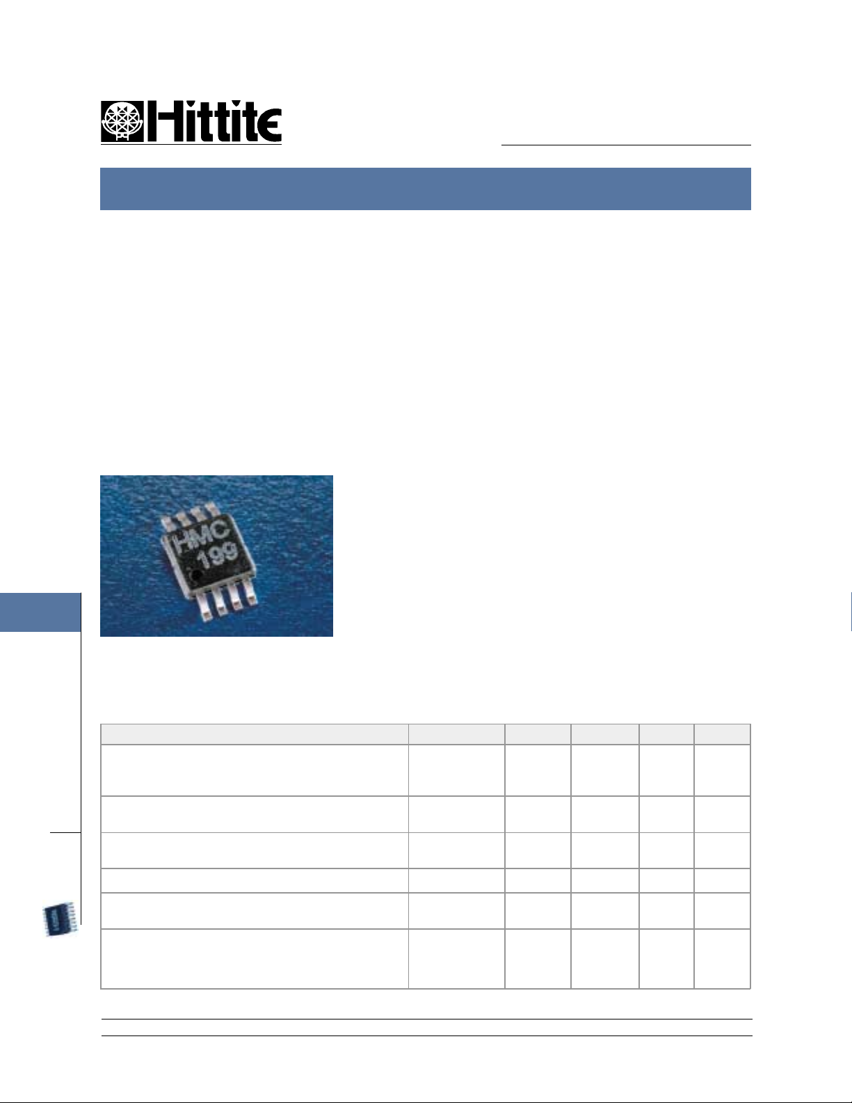
HMC199MS8 MSOP8 DUAL SPDT SWITCH DC - 2.5 GHz
HMC199MS8
7
FEBRUARY 2001
Features
INTEGRATED DUAL SPDTs
LOW INSERTION LOSS: <0.5 dB @ 2.0 GHz
POSITIVE CONTROL: 0/+5V
ULTRA SMALL MSOP8 PACKAGE: 14.8 mm
V01.0700
General Description
The HMC199MS8 is a low-cost dual SPDT
GaAs “bypass” switch in an 8-lead MSOP
package covering DC to 2.5 GHz. This
four RF port component integrates two
SPDT switches and a through line onto a
2
single IC. The design provides low insertion loss of less than 0.5 dB while switching passive or active external circuit components in and out of the signal path. Port
to port isolations are typically 35 to 20 dB.
On-chip circuitry enables positive voltage
control operation at very low DC currents
with control inputs compatible with CMOS
and most TTL logic families. Applications
include LNA or filter bypass switching and
single bit attenuator switching for cellular,
PCS, and ISM base stations.
Guaranteed Performance Vctl = 0/ +5 Vdc, 50 Ohm System, -40 to +85 deg. C
SWITCHES
Insertion Loss
SPDT
Isolation
Return Loss (On State, Any P ort) DC - 2.0 GHz
Input Power for 1dB Compression 0.5 - 2.0 GHz 19 23 dBm
SMT
Input ThirdOrderIntercept
(Two Tone I nput Power= 0 dBm Each Tone)
Switching Characteristics
tRISE / tFALL (10/90% RF / 90/10% RF)
tON / tOFF (50% CTL to 10/90% RF)
12 Elizabeth Drive, Chelmsford, MA 01824 Phone: 978-250-3343 Fax: 978-250-3373 Web Site: www.hittite.com
7 - 70
Parameter Frequency Min. Typ. Max. Units
DC - 1.0 GHz
DC - 2.0 GHz
DC - 2.5 GHz
DC - 2.0 GHz
DC - 2.5 GHz
DC - 2.5 GHz
0.5 - 2.0 GHz 32 36 dBm
DC - 2. 5 GHz
22
17
22
14
0.3
0.5
0.7
25
21
25
17
20
40
0.6
0.8
1.0
dB
dB
dB
dB
dB
dB
dB
nS
nS
Page 2
MICROWAVE CORPORATION
HMC199MS8 MSOP8 DUAL SPDT SWITCH DC - 2.5 GHz
H MC199MS8
'99
new!
V01.0700
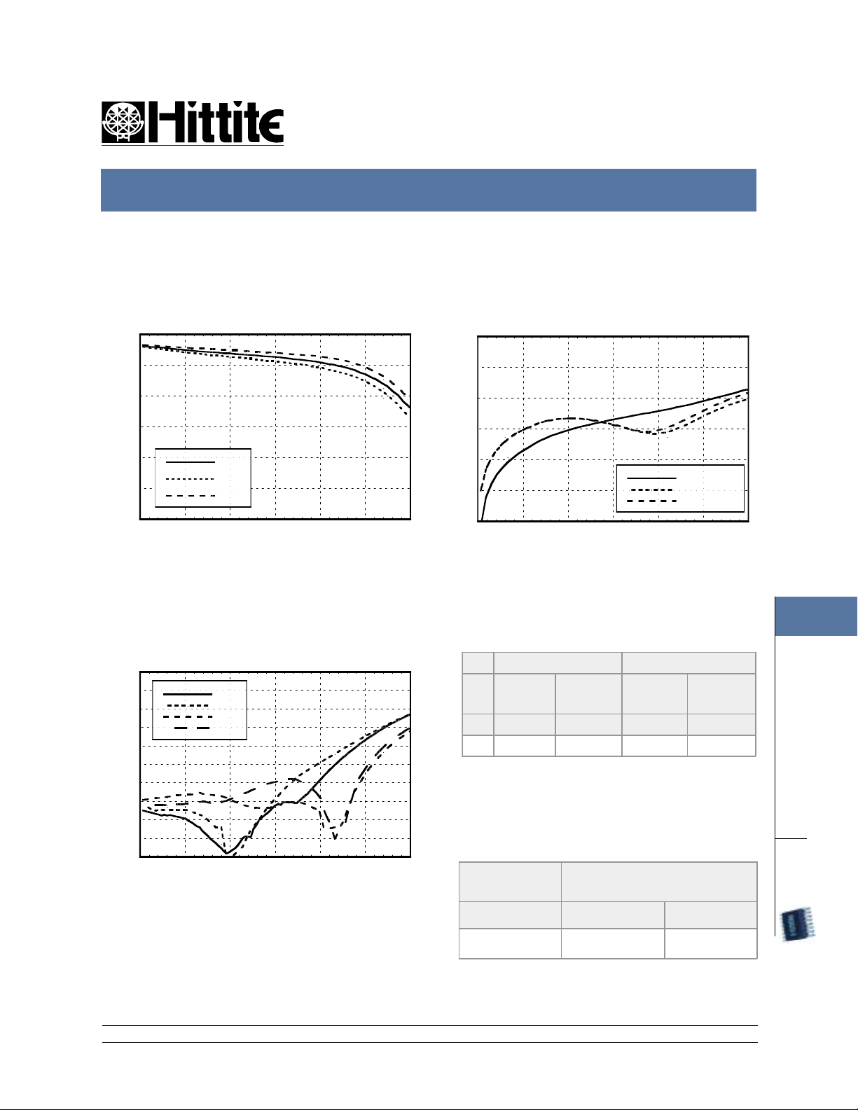
Insertion Loss
0
-0.5
-1
-1.5
-2
INSERTION LOSS (dB)
-2.5
-3
0 0.5 1 1.5 2 2.5 3
+25 C
+85 C
-40 C
FREQUENCY (GHz)
Return Loss
0
-5
-10
-15
-20
-25
-30
-35
RETURN LOSS (dB)
-40
-45
-50
0 0.5 1 1.5 2 2.5 3
RFC1
RFC2
RF1
RF2
FREQUENCY (GHz)
FEBRUARY 2001
Isolation
0
-10
-20
-30
-40
ISOLATION (dB)
RFC1 to RFC2
-50
-60
0 0.5 1 1.5 2 2.5 3
FREQUENCY (GHz)
RFC1 to RF1
RFC2 to RF2
Note: Isolation between RF1 - RF2 ( when RFC1 RFC2 is in insertion loss state) is 25 dB @ 1 GHz
and 17 dB @ 2 GHz.
Compression vs Frequency
Carrier at 900MHz Carrier at 1900MHz
InputPower
CTL
for 0.1dB
Input
Compression
(Vdc) (dBm) (dBm) (dBm) (dBm)
+5 20 23.5 19 22
InputPower
for 1dB
Compression
InputPower
for 0.1dB
Compression
InputPower
Compression
Caution: Do not operate continuously at RF power
input greater than 1dB compression and do not "hot
switch" power levels greater than +13 dBm
(Control =0/ +5Vdc).
Distortion vs Frequency
Control Input
Input Third Order Intercept (dBm)
0 dBm Each Tone
7
for 1dB
SWITCHES
SPDT
SMT
(Vdc) 900 MHz 1900 MHz
+5 34.5 37.5
12 Elizabeth Drive, Chelmsford, MA 01824 Phone: 978-250-3343 Fax: 978-250-3373 Web Site: www.hittite.com
7 - 71
Page 3

'99
new!
MICROWAVE CORPORATION
HMC199MS8 MSOP8 DUAL SPDT SWITCH DC - 2.5 GHz
FEBRUARY 2001
Functional Diagram
RF1 GND GND RF2
PIN1
RFC1 A B RFC2
HMC199MS8
V01.0700
Absolute Maximum Ratings
RF Input Power Vctl = 0/+5V +24 dBm
Control Voltage Range (A & B) -0.5 to +7.5 Vdc
Storage T emperature -65 to +150 deg C
Operating Temperature -40 to +85 dec C
T ruth Table
*Control Input Tolerances are +/- 0.5 Vdc
Control Input *
A
(Vdc)B(Vdc)Ia(uA)Ib(uA)
0 +5 -65 65 On Off Off
+5 0 65 -65 Off On On
Control Current
(Typical)
RFC1
to
RFC2
SignalPath
RFC1
to
RF1
RFC2
to
RF2
Outline Drawing
7
SWITCHES
SPDT
SMT
1. MATERIAL:
A) PACKAGE BODY - LOW STRESS INJECTION-MOLDED PLASTIC.
B) LEADFRAME MATERIAL: COPPER ALLOY
2 . PLATING : LEAD - TIN SOLDER PLATE
3. DIMENSIONS ARE IN INCHES (MILLIMETERS).
UNLESS OTHERWISE SPECIFIED ALL TOL. ARE ±0.005(±0.13).
DC blocking capacitors are required at ports RFC1,
RFC2, RF1, RF2. Choose value for lowest frequency of
operation.
4. DIMENSION DOES NOT INCLUDE MOLDFLASH OF 0.15 MM PER SIDE
5. DIMENSION DOES NOT INCLUDE MOLDFLASH OF 0.25 MM PER SIDE
12 Elizabeth Drive, Chelmsford, MA 01824 Phone: 978-250-3343 Fax: 978-250-3373 Web Site: www.hittite.com
7 - 72
Page 4

MICROWAVE CORPORATION
HMC199MS8 MSOP8 DUAL SPDT SWITCH DC - 2.5 GHz
new!
HMC199MS8
'99
V01.0700
Eval Board Layout (Top View)
FEBRUARY 2001
* R1 & R2 = 100 Ω .
These optional resistors will
provide more RF path to control
circuit isolation.
7
The circuit board used in the final application should be generated with proper RF circuit design techniques.
Signal lines at the RF port should have 50 ohm impedance. The evaluation circuit board shown above is
available from Hittite Microwave Corporation upon request.
List of Material
Item Description
J1 - J4 PC Mount SMA Connector
J5- J8 DC Pin
C1 - C4 Chip Capacitor, 0402 Pkg.Choose value for lowest frequency
of operation. 330 pF is provided on PCB.
R1 - R2 100 ohm Resister, 0402 Pkg.
U1 HMC199MS8 BypassSwitch
PCB* 103234 Evaluation PCB 1.5" x 1.5"
* Circuit Board Material : Rogers 4350
12 Elizabeth Drive, Chelmsford, MA 01824 Phone: 978-250-3343 Fax: 978-250-3373 Web Site: www.hittite.com
7 - 73
SWITCHES
SPDT
SMT
Page 5

'99
new!
MICROWAVE CORPORATION
HMC199MS8 MSOP8 DUAL SPDT SWITCH DC - 2.5 GHz
FEBRUARY 2001
Typical Application Circuit
RF2
RF1
HMC199MS8
V01.0700
C4
GND
GND
C2
PIN 1
Vdd
C3
RFC2
B
A
C1
RFC1
Notes:
7
1. Set A / B control to 0/+5V, Vdd = +5V and use HCT series logic to provide a TTL driver interface.
2. Control inputs A/B can be driven directly with CMOS logic (HC) with Vdd = 5 to 7 Volts applied to the CMOS logic gates.
3. DC Blocking capacitors are required for each RF port as shown. Capacitor value determines lowest frequency of operation.
4. Highest RF signal power capability is achieved with Vdd = +7V and A/B set to 0/+7V.
SWITCHES
SPDT
SMT
CTL
74HC04 or
74HCT04
12 Elizabeth Drive, Chelmsford, MA 01824 Phone: 978-250-3343 Fax: 978-250-3373 Web Site: www.hittite.com
7 - 74
Page 6

MICROWAVE CORPORATION
HMC199MS8 MSOP8 DUAL SPDT SWITCH DC - 2.5 GHz
new!
HMC199MS8
'99
V01.0700
NOTES:
FEBRUARY 2001
7
12 Elizabeth Drive, Chelmsford, MA 01824 Phone: 978-250-3343 Fax: 978-250-3373 Web Site: www.hittite.com
7 - 75
SWITCHES
SPDT
SMT
 Loading...