

Page 1

'99
new!
MICROWAVE CORPORATION
HMC197
GaAS MMIC SOT26 SPDT SWITCH DC - 3 GHz
7
FEBRUARY 2001
Features
LOW INSERTION LOSS: 0.4 dB
ULTRA SMALL PACKAGE: SOT26
INPUT IP3: +45 dBm
POSITIVE CONTROL: 0/+3V @ 10 µA
V01.0700
General Description
The HMC197 is a low-cost SPDT switch in a 6lead SOT26 plastic package for use in general
switching applications which require very low
insertion loss and very small size. The device
can control signals from DC to 3.0 GHz and is
especially suited for 900 MHz, 1.8-2.2GHz, and
2.4GHz ISM applications with less than 1dB
loss. The design provides exceptional insertion
loss performance, ideal for filter and receiver
switching. RF1 or RF2 is a reflective short when
"Off". The two control voltages require a minimal
amount of DC current and offer compatibility
with most CMOS & TTL logic families. The
HMC197 is especially suited for PCMCIA wireless card and cellular phone applications. See
HMC221 for same performance in an alternate
SOT26 pin-out.
Guaranteed Performance Vctl = 0/+3 to +8 Vdc, -40 to +85 deg C
retemaraP ycneuqerF .niM .pyT .xaM stinU
SWITCHES
SPDT
ssoLnoitresnI
noitalosI
ssoLnruteR
SMT
)V5+/0=ltcV(
scitsiretcarahCgnihctiwS
12 Elizabeth Drive, Chelmsford, MA 01824 Phone: 978-250-3343 Fax: 978-250-3373 Web Site: www.hittite.com
noisserpmoCBd1rofrewoPtupnI
tpecretnIredrOdrihTtupnI
)enothcaemBd7+,V5+/0=ltcV(
)FR%09/01(LLAFt,ESIRt
)FR%09/01otLTC%05(FFOt,NOt
zHG0.1-CD
zHG0.2-CD
zHG5.2-CD
zHG0.3-CD
zHG0.1-CD
zHG0.2-CD
zHG5.2-CD
zHG0.3-CD
zHG0.1-CD
zHG0.2-CD
zHG5.2-CD
zHG0.3-CD
zHG0.1-5.0
zHG0.3-5.0
zHG0.1-5.0
zHG0.3-5.0
zHG0.3-CD
42
42
81
41
02
61
41
01
52
32
04
83
7 - 64
4.0
54.0
7.0
8.0
82
82
22
81
03
22
71
31
03
92
54
34
3
01
7.0
8.0
9.0
1.1
Bd
Bd
Bd
Bd
Bd
Bd
Bd
Bd
Bd
Bd
Bd
Bd
mBd
mBd
mBd
mBd
Sn
Sn
Page 2
MICROWAVE CORPORATION
HMC197 SOT26 SPDT SWITCH DC - 3 GHz
HMC197
'99
new!
V01.0700
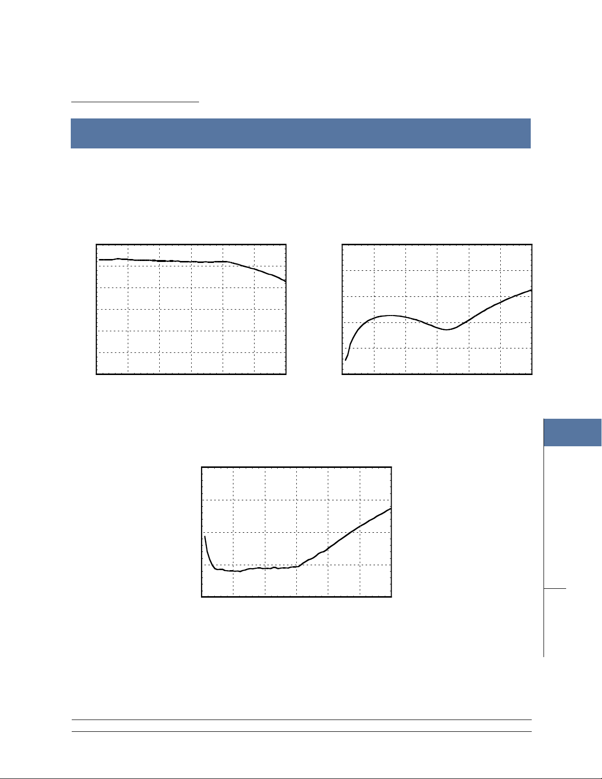
Insertion Loss
0
-0.5
-1
-1.5
-2
INSERTION LOSS (dB)
-2.5
-3
0 0.5 1 1.5 2 2.5 3
FREQUENCY (GHz)
Isolation
ISOLATION (dB)
Return Loss
FEBRUARY 2001
0
-10
-20
-30
-40
-50
0 0.5 1 1.5 2 2.5 3
FREQUENCY (GHz)
7
0
-10
-20
RETURN LOSS(dB)
-30
-40
0 0.5 1 1.5 2 2.5 3
FREQUENCY (GHz)
12 Elizabeth Drive, Chelmsford, MA 01824 Phone: 978-250-3343 Fax: 978-250-3373 Web Site: www.hittite.com
7 - 65
SWITCHES
SPDT
SMT
Page 3

'99
new!
MICROWAVE CORPORATION
HMC197 SOT26 SPDT SWITCH DC - 3 GHz
FEBRUARY 2001
Input 0.1 and 1.0 dB
Compression vs Control Voltage
35
1 dB at 900 MHz
30
25
20
COMPRESSION (dBm)
INPUT POWER FOR 0.1 AND 1 dB
15
3456789
1 dB at 1900 MHz
0.1 dB at 1900 MHz
CONTROL INPUT (Vdc)
0.1 dB at 900 MHz
HMC197
Input Third Order Intercept vs
Control Voltage
48
46
44
42
INTERCEPT(dBm)
INPUT THIRD ORDER
40
38
23456789
900 MHz
1900 MHz
CONTROL INPUT (Vdc)
V01.0700
7
Compression vs Control Voltage
SWITCHES
SPDT
SMT
Caution: Do not operate in 1dB compression at power levels
above +31 dBm ( Vctl= +5 Vdc) and do not 'hot switch' power
levels greater than +20 dBm (V
DC blocks are required at ports RFC, RF1 and RF2.
zHM009tareirraC zHM0091tareirraC
lortnoC
tupnI
)cdV( )mBd( )mBd( )mBd( )mBd(
3+71027102
5+52034292
8+13330323
rewoPtupnI
Bd1.0rof
noisserpmoC
rewoPtupnI
Bd1rof
noisserpmoC
= +5Vdc).
CTL
rewoPtupnI
Bd1.0rof
noisserpmoC
Distortion vs Control Voltage
ControlInput
rewoPtupnI
Bd1rof
noisserpmoC
(Vdc) 900 MHz 1900 MHz
+3 41 39
+5 45 43
+8 46 44
Third Order Intercept (dBm)
+7 dBm Each Tone
12 Elizabeth Drive, Chelmsford, MA 01824 Phone: 978-250-3343 Fax: 978-250-3373 Web Site: www.hittite.com
7 - 66
Page 4

MICROWAVE CORPORATION
HMC197 SOT26 SPDT SWITCH DC - 3 GHz
HMC197
'99
new!
V01.0700
Functional Diagram
RF2
B
RF
PIN 1
A
RF1
GND
Absolute Maximum Ratings
)B&A(egnaRegatloVlortnoCcdV21+ot2.0-
erutarepmeTegarotSC.ged051+ot56-
erutarepmeTgnitarepOC.ged58+ot04-
Outline
FEBRUARY 2001
Truth T able *Control Input T olerances are +/- 0.2 Vdc
*tupnIlortnoC
A
03+01-01nOffO
05+55-55nOffO
07+012-012nOffO
08+082-082nOffO
B
)cdV(
3+00101-ffOnO
5+05555-ffOnO
7+0012012-ffOnO
8+0082082-ffOnO
aI
)cdV(
lortnoC
tnerruC
bI
)Au(
)Au(
otFR
1FR
htaPlangiS
otFR
2FR
7
1) MATERIAL:
A) PACKAGE BODY: LOW STRESS INJECTION MOLDED PLASTIC,
SILICA & SILICONE IMPREGNATED
B) LEADFRAME MATERIAL: COPPER ALLOY
2 . PLATING: LEAD-TIN SOLDER PLATE
3. DIMENSIONS ARE IN INCHES (MILLIMETERS)
UNLESS OTHERWISE SPECIFIED TOL. ARE ±0.005(±0.13)
12 Elizabeth Drive, Chelmsford, MA 01824 Phone: 978-250-3343 Fax: 978-250-3373 Web Site: www.hittite.com
7 - 67
SWITCHES
SPDT
SMT
Page 5

'99
new!
MICROWAVE CORPORATION
HMC197 SOT26 SPDT SWITCH DC - 3 GHz
FEBRUARY 2001
Typical Application Circuit
RF1
RFC
Pin 1
GND
HMC197
V01.0700
A
B
RF2
+Vdd
Notes:
7
1. Set logic gate and switch Vdd = +3V to +5V and use HCT series logic to provide a TTL driver interface.
2. Control inputs A/B can be driven directly with CMOS logic (HC) with Vdd of 5 to 8 Volts applied to the CMOS logic gates.
3. DC Blocking capacitors are required for each RF port as shown. Capacitor value determines lowest frequency of operation.
4. Highest RF signal power capability is achieved with Vdd = +8V and A/B set to 0/+8V.
SWITCHES
SPDT
SMT
CTL
74HC04 or
74HCT04
12 Elizabeth Drive, Chelmsford, MA 01824 Phone: 978-250-3343 Fax: 978-250-3373 Web Site: www.hittite.com
7 - 68
Page 6

MICROWAVE CORPORATION
HMC197 SOT26 SPDT SWITCH DC - 3 GHz
HMC197
'99
new!
V01.0700
FEBRUARY 2001
Evaluation Circuit Board
The circuit board used in the final application should use RF circuit design techniques. Signal lines should
have 50 ohm impedance while the package ground leads should be connected directly to the ground plane
similar to that shown below. A sufficient number of VIA holes should be used to connect the top and bottom
ground planes. The evaluation circuit board as shown is available from Hittite upon request.
7
Evaluation Circuit Board Layout Design Details
Layout Technique Grounded Co-Planar Waveguide (GCPW)
Material FR4
Dielectric Thickness 0.028" (0.71 mm)
50 Ohm Line Width 0.037" (0.94 mm)
Gap to Ground Edge 0.010" (0.25 mm)
Ground VIA Hole Diameter 0.014" (0.36 mm)
Connectors SMA-F ( EF - Johnson P/N 142-0701-806)
12 Elizabeth Drive, Chelmsford, MA 01824 Phone: 978-250-3343 Fax: 978-250-3373 Web Site: www.hittite.com
7 - 69
SWITCHES
SPDT
SMT
 Loading...