

Page 1
查询HMC194MS8供应商
14
MICROWAVE CORPORATION
Typical Applications
The HMC194MS8 is ideal for:
• Cellular/PCS Base Stations
• Portable Wireless
• MMDS & WirelessLAN
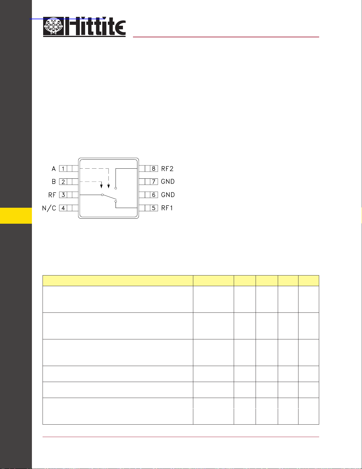
Functional Diagram
v04.0903
HMC194MS8
GaAs MMIC SPDT SWITCH
DC - 3 GHz
Features
Ultra Small Package: MSOP8
High Isolation: 50 dB
Positive Control: 0/+3V to 0/+7V
General Description
The HMC194MS8 is a low-cost SPDT switch in
an 8-lead MSOP package for use in applications which require high isolation between two
RF paths. The device can control signals from
DC to 3 GHz and has been optimized to provide
extremely high isolation with minimal insertion
loss in medium and low power applications. On
chip circuitry allows positive voltage control operation at very low DC currents with control inputs
compatible with CMOS and most TTL logic families. RF1 and RF2 are refl ective opens when
“OFF”.
Electrical Specifi cations, T
Insertion Loss
SWITCHES - SMT
Isolation
Return Loss
Input Power for 1 dB Compression
0/+5V Control
Input Third Order Intercept
(Two-tone Input Power = +7 dBm Each Tone)
Switching Characteristics DC - 3.0 GHz
= +25° C, Vctl = 0/+5 Vdc, 50 Ohm System
A
Parameter Frequency Min. Typ. Max. Units
RF1 / RF2
RF1 / RF2
0/+5V Control 0.5 - 1.0 GHz
tRISE, tFALL (10/90% RF)
tON , tOFF (50% CTL to 10/90% RF)
DC - 1.0 GHz
DC - 2.0 GHz
DC - 2.5 GHz
DC - 3.0 GHz
DC - 1.0 GHz
DC - 2.0 GHz
DC - 2.5 GHz
DC - 3.0 GHz
DC - 1.0 GHz
DC - 2.0 GHz
DC - 2.5 GHz
DC - 3.0 GHz
0.5 - 1.0 GHz
0.5 - 3.0 GHz
0.5 - 3.0 GHz
45 / 47
39 / 43
31
24
18
14
13
13
19
17
39
37
0.7
0.7
0.8
0.9
49 / 51
42 / 46
35
28
21
17
17
17
23
21
43
41
10
24
0.9
0.9
1.1
1.4
dB
dB
dB
dB
dB
dB
dB
dB
dB
dB
dB
dB
dBm
dBm
dBm
dBm
ns
ns
14 - 42
For price, delivery, and to place orders, please contact Hittite Microwave Corporation:
12 Elizabeth Drive, Chelmsford, MA 01824 Phone: 978-250-3343 Fax: 978-250-3373
Order Online at www.hittite.com
Page 2
v04.0903
HMC194MS8
MICROWAVE CORPORATION
GaAs MMIC SPDT SWITCH
DC - 3 GHz
GaAs MMIC SUB-HARMONICALLY PUMPED MIXER 17 - 25 GHz
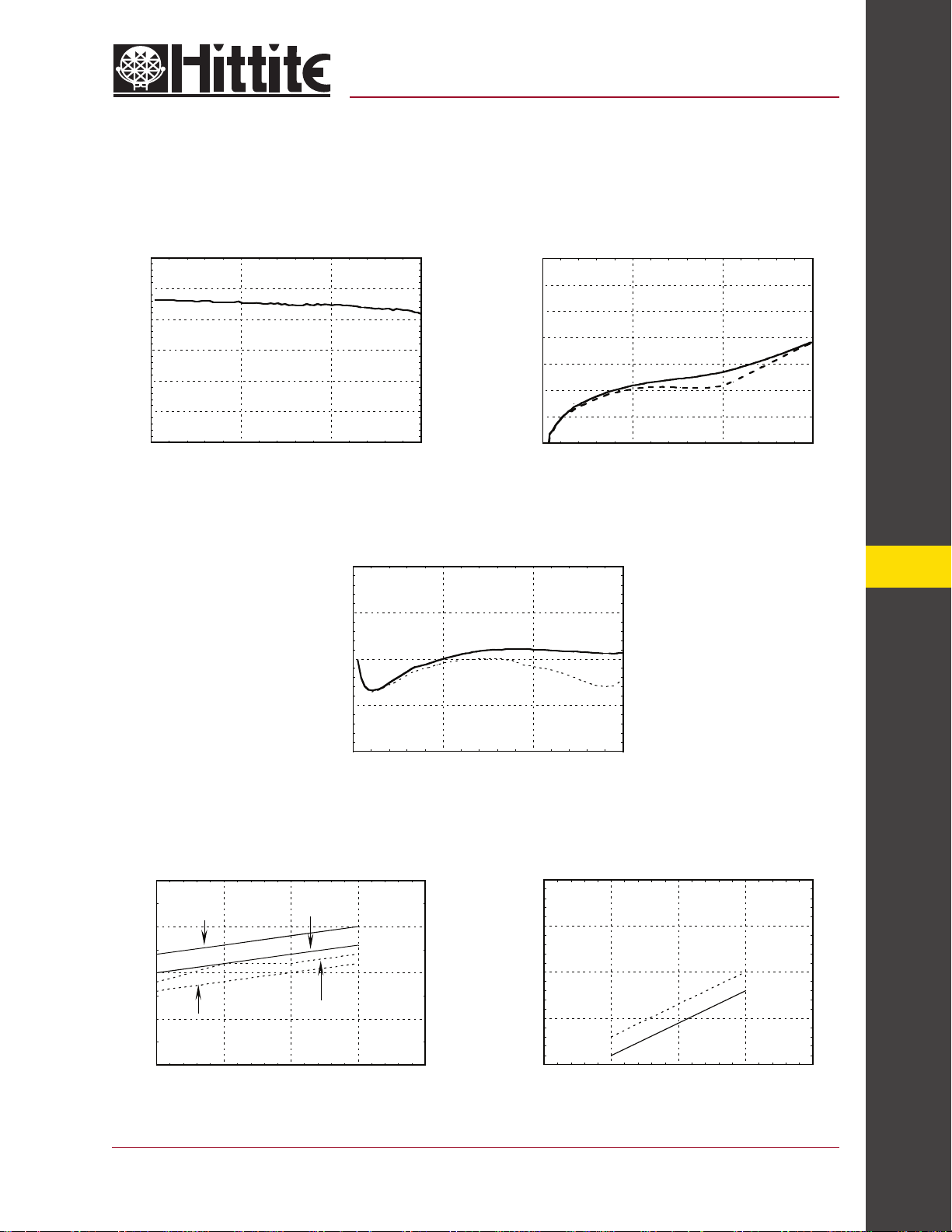
Insertion Loss
Isolation
0
-0.5
-1
-1.5
-2
INSERTION LOSS (dB)
-2.5
-3
0123
FREQUENCY (GHz)
Return Loss
0
-10
-20
RETURN LOSS (dB)
-30
0
-10
-20
-30
-40
ISOLATION (dB)
-50
-60
-70
0123
S22
S11
RF1
FREQUENCY (GHz)
RF2
14
-40
0123
Input 0.1 and 1.0 dB
Compression vs. Control Voltage
30
P1 dB at 900 MHz
25
20
15
P0.1 dB at 1900 MHz
10
45678
INPUT POWER FOR 0.1 & 1dB COMPRESSION
For price, delivery, and to place orders, please contact Hittite Microwave Corporation:
12 Elizabeth Drive, Chelmsford, MA 01824 Phone: 978-250-3343 Fax: 978-250-3373
P1 dB at 1900 MHz
P0.1 dB at 900 MHz
Control Input (Vdc)
Order Online at www.hittite.com
FREQUENCY (GHz)
Input Third Order
Intercept Point vs. Control Voltage
INPUT THIRD ORDER INTERCEPT (dBm)
60
55
50
900 MHz
45
1900 MHz
40
45678
Control Input (Vdc)
SWITCHES - SMT
14 - 43
Page 3

MICROWAVE CORPORATION
v04.0903
Compression vs. Control Voltage
Carrier at 900 MHz Carrier at 1900 MHz
HMC194MS8
GaAs MMIC SPDT SWITCH
DC - 3 GHz
Input Power
Bias
Vdd
(Vdc) (dBm) (dBm) (dBm) (dBm)
for 0.1 dB
Compression
+4 19 22 18 20
+5 21 23 19 21
+6 21 24 20 22
+7 22 25 21 23
Distortion vs. Control Voltage
Control Input
14
(Vdc) 900 MHz 1900 MHz
+5 43 41
+7 50 48
Truth Table
*Control Input Voltage Tolerances are ± 0.2 Vdc.
Control Input* Control Current Signal Path State
A
(Vdc)B(Vdc)
0 +3 -23 +23 ON OFF
+3 0 +23 -23 OFF ON
0 +5 -95 +95 ON OFF
SWITCHES - SMT
+5 0 +95 -95 OFF ON
0 +7 -190 +190 ON OFF
+7 0 +190 -190 OFF ON
Input Power
for 1.0 dB
Compression
Third Order Intercept (dBm)
Ia
(uA)
Input Power
for 0.1 dB
Compression
+7 dBm Each Tone
Ib
(uA)
RF to
RF1
Input Power
for 1.0 dB
Compression
RF to
RF2
Caution: Do not operate in 1dB compression at power levels
above +25 dBm and do not “hot switch” power levels greater
than +18 dBm (Control = 0/+5Vdc).
DC blocks are required at ports RFC, RF1 and RF2.
14 - 44
For price, delivery, and to place orders, please contact Hittite Microwave Corporation:
12 Elizabeth Drive, Chelmsford, MA 01824 Phone: 978-250-3343 Fax: 978-250-3373
Order Online at www.hittite.com
Page 4

MICROWAVE CORPORATION
v04.0903
Absolute Maximum Ratings
Control Voltage Range (A & B) -0.2 to +7.5 Vdc
Storage Temperature -65 to +150 °C
Operating Temperature -40 to +85 °C
Outline Drawing
HMC194MS8
GaAs MMIC SPDT SWITCH
DC - 3 GHz
NOTES:
1. PACKAGE BODY MATERIAL: LOW STRESS INJECTION MOLDED
PLASTIC SILICA AND SILICON IMPREGNATED.
2. LEADFRAME MATERIAL: COPPER ALLOY
3. LEADFRAME PLATING: Sn/Pb SOLDER
4. DIMENSIONS ARE IN INCHES [MILLIMETERS].
5. DIMENSION DOES NOT INCLUDE MOLDFLASH OF 0.15mm PER SIDE.
6. DIMENSION DOES NOT INCLUDE MOLDFLASH OF 0.25mm PER SIDE.
7. ALL GROUND LEADS MUST BE SOLDERED TO PCB RF GROUND.
14
SWITCHES - SMT
For price, delivery, and to place orders, please contact Hittite Microwave Corporation:
12 Elizabeth Drive, Chelmsford, MA 01824 Phone: 978-250-3343 Fax: 978-250-3373
Order Online at www.hittite.com
14 - 45
Page 5

v04.0903
MICROWAVE CORPORATION
Typical Application Circuit
HMC194MS8
GaAs MMIC SPDT SWITCH
DC - 3 GHz
14
Notes:
1. Set logic gate and switch Vdd = +3V to +5V and use HCT series logic to provide a TTL driver interface.
2. Control inputs A/B can be driven directly with CMOS logic (HC) with Vdd of 3 to 7 Volts applied to the CMOS
logic gates.
3. DC Blocking capacitors are required for each RF port as shown. Capacitor value determines lowest frequency
SWITCHES - SMT
of operation.
4. Highest RF signal power capability is achieved with Control set to 0/+7V.
See “Design Techniques Enhance Isolation in Switch Assemblies”
for HMC194MS8 Applications, “Application Notes” Section.
14 - 46
For price, delivery, and to place orders, please contact Hittite Microwave Corporation:
12 Elizabeth Drive, Chelmsford, MA 01824 Phone: 978-250-3343 Fax: 978-250-3373
Order Online at www.hittite.com
Page 6

MICROWAVE CORPORATION
Evaluation Circuit Board
v04.0903
HMC194MS8
GaAs MMIC SPDT SWITCH
DC - 3 GHz
List of Material
Item Description
J1 - J3 PC Mount SMA RF Connector
J4 - J6 DC Pin
C1 - C3 100 pF capacitor, 0402 Pkg.
R1, R2
U1 HMC194MS8 SPDT Switch
PCB* 107821 Evaluation PCB
* Circuit Board Material: Rogers 4350
100 Ω
resistor, 0402 Pkg.
The circuit board used in the fi nal application
should be generated with proper RF circuit design
techniques. Signal lines at the RF port should
have 50 ohm impedance and the package ground
leads should be connected directly to the ground
plane similar to that shown above. The evaluation circuit board shown above is available from
Hittite Microwave Corporation upon request.
14
SWITCHES - SMT
For price, delivery, and to place orders, please contact Hittite Microwave Corporation:
12 Elizabeth Drive, Chelmsford, MA 01824 Phone: 978-250-3343 Fax: 978-250-3373
Order Online at www.hittite.com
14 - 47
 Loading...