

Page 1
'99
new!
MICROWAVE CORPORATION
HMC190MS8
GaAS MMIC MSOP8 SPDT SWITCH DC - 3 GHz
7
FEBRUARY 2001
Features
LOW INSERTION LOSS: 0.4 dB
ULTRA SMALL PACKAGE: MSOP8
HIGH INPUT IP3 : +50 dBm
POSITIVE CONTROL: 0/+3V @ 10 µA
V01.0700
General Description
The HMC190MS8 is a low cost SPDT switch
in an 8-lead MSOP package. The switch
can control signals from DC to 3.0 GHz. It is
especially suited for low and medium power
applications using positive control voltages.
The two control voltages require a minimal
amount of DC current, which is optimal for
battery powered radio systems at 0.9, 1.9,
and 2.4 GHz.
The HMC190MS8 design provides exceptional third order intermodulation performance of +50 dBm. The design has been
optimized for the small MSOP package, and
maintains a VSWR of better than 1.2:1 up to
2 GHz. This device is the positive control
MSOP8 packaged version of our
HMC239S8 negative control device.
Guaranteed Performance Vctl = 0/+3 to +8 Vdc, -40 to +85 deg C
retemaraP ycneuqerF .niM .pyT .xaM stinU
SWITCHES
esnIssoLnoitr
SPDT
SMT
12 Elizabeth Drive, Chelmsford, MA 01824 Phone: 978-250-3343 Fax: 978-250-3373 Web Site: www.hittite.com
noitalosI
ssoLnruteR
noisserpmoCBd1rofrewoPtupnI
)V5+/0=ltcV(
tpecretnIredrOdrihTtupnI
)enoThcaEmBd7+,V5+/0=ltcV(
hCgnihctiwSrascitsiretca
)FR%01/09/FR%09/01(LLAFt/ESIRt
%05(FFOt/NOtR%09/01otLTC)F
zHG0.1-CD
zHG0.2-CD
zHG5.2-CD
zHG0.3-CD
zHG0.1-CD
zHG0.2-CD
zHG5.2-CD
zHG0.3-CD
zHG0.1-CD
zHG0.2-CD
zHG5.2-CD
zHG0.3-CD
zHG0.1-5.0
zHG0.3-5.0
zHG0.1-5.0
zHG0.3-5.0
zHG0.3-CD
32
32
22
91
42
02
51
01
52
32
54
44
7 - 46
4.0
4.0
5.0
7.0
72
72
62
22
82
82
02
61
03
92
05
94
3
01
6.0
6.0
8.0
0.1
Bd
Bd
Bd
Bd
Bd
Bd
Bd
Bd
Bd
Bd
Bd
Bd
mBd
mBd
mBd
mBd
Sn
Sn
Page 2
MICROWAVE CORPORATION
HMC190MS8 MSOP8 SPDT SWITCH DC - 3 GHz
new!
HMC190MS8
'99
V01.0700
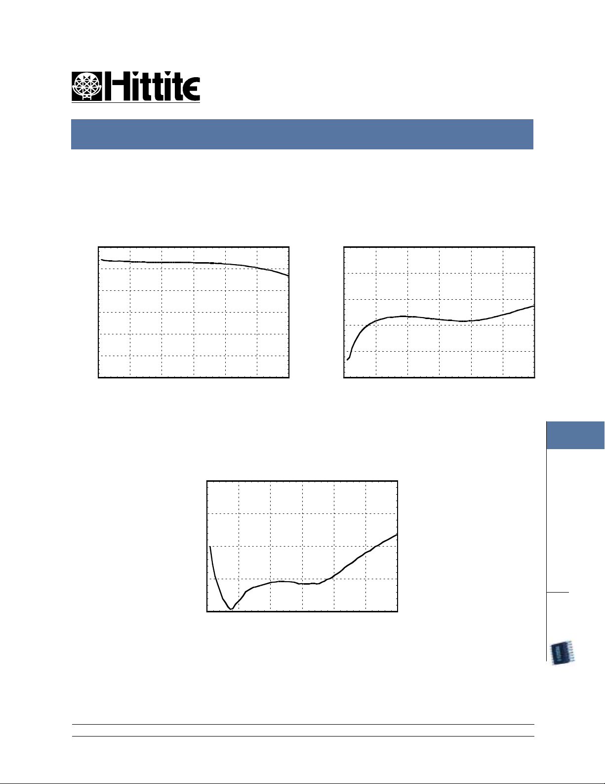
Insertion Loss
0
-0.5
-1
-1.5
-2
INSERTION LOSS (dB)
-2.5
-3
0 0.5 1 1.5 2 2.5 3
FREQUENCY (GHz)
FEBRUARY 2001
Isolation
0
-10
-20
-30
ISOLATION (dB)
-40
-50
0 0.5 1 1.5 2 2.5 3
FREQUENCY (GHz)
7
Return Loss
0
-10
-20
-30
INPUT RETURN LOSS (dB)
-40
0 0.5 1 1.5 2 2.5 3
FREQUENCY (GHz)
12 Elizabeth Drive, Chelmsford, MA 01824 Phone: 978-250-3343 Fax: 978-250-3373 Web Site: www.hittite.com
SWITCHES
SPDT
SMT
7 - 47
Page 3

'99
new!
MICROWAVE CORPORATION
HMC190MS8 MSOP8 SPDT SWITCH DC - 3 GHz
FEBRUARY 2001
Input 0.1 and 1.0 dB
Compression vs Control Voltage
35
1 dB at 900 MHz
30
25
20
COMPRESSION (dBm)
INPUT POWER FOR 0.1 AND 1 dB
15
3456789
1 dB at 1900 MHz
0.1 dB at 1900 MHz
CONTROL INPUT (Vdc)
0.1 dB at 900 MHz
HMC190MS8
V01.0700
Input Third Order Intercept
Point vs Control Voltage
55
53
51
49
INTERCEPT(dBm)
INPUT THIRD ORDER
47
45
456789
900 MHz
1900 MHz
CONTROL INPUT (Vdc)
7
Compression vs Control Voltage
SWITCHES
SPDT
Caution: Do not operate in 1dB compression at power
SMT
levels above +31 dBm (Vctl=+5 Vdc) and do not 'hot
switch' power levels greater than +20dBm (V
DC blocks are required at ports RFC, RF1 and RF2.
zHM009tareirraC zHM0091tareirraC
lortnoC
tupnI
)cdV( )mBd( )mBd( )mBd( )mBd(
3+71027102
5+52034292
8+13330323
rewoPtupnI
Bd1.0rof
noisserpmoC
rewoPtupnI
Bd1rof
noisserpmoC
rewoPtupnI
Bd1.0rof
noisserpmoC
= +5Vdc).
CTL
Distortion vs Control Voltage
tupnIlortnoC
rewoPtupnI
Bd1rof
noisserpmoC
)cdV( zHM009 zHM0091
5+0594
8+3515
)mBd(tpecretnIredrOdrihT
enoThcaEmBd7+
12 Elizabeth Drive, Chelmsford, MA 01824 Phone: 978-250-3343 Fax: 978-250-3373 Web Site: www.hittite.com
7 - 48
Page 4

MICROWAVE CORPORATION
HMC190MS8 MSOP8 SPDT SWITCH DC - 3 GHz
new!
HMC190MS8
'99
V01.0700
Functional Diagram
PIN 1
GND
RFC
GND
RF2GND
RF1
B
A
Absolute Maximum Ratings
V
LTC
rewoPtupnI.xaM
V8+/0=
erutarepmeTegarotSC.ged051+ot56-
zHG50.0
zHG2-5.0
)B&A(egnaRegatloVlortnoCcdV21+ot2.0-
mBd72+
mBd43+
FEBRUARY 2001
Truth Table *Control Input T olerances are +/- 0.2 Vdc
*tupnIlortnoC
A
03+01-01nOffO
05+55-55nOffO
07+012-012nOffO
08+082-082nOffO
B
)cdV(
3+00101-ffOnO
5+05555-ffOnO
7+0012012-ffOnO
8+0082082-ffOnO
aI
)cdV(
lortnoC
tnerruC
bI
)Au(
)Au(
otFR
1FR
htaPlangiS
otFR
2FR
7
erutarepmeTgnitarepOC.ged58+ot04-
RF2
RF1
0.116/0.120
(2.95/3.05)
B
A
0.032/0.036
(0.81/0.91)
0.012 TYP
(0.30)
0.188/0.196
(4.78/4.98)(2.95/3.05)
0-5 DEG
XXXX
YYWW
0.021 MIN TYP
(0.53)
LOT NUMBER
DATE CODE
YY= YEAR
WW= WEEK
PIN 1 (REF)
0.005/0.007
(0.13/0.18)
1) MATERIAL:
A) PACKAGE BODY: LOW STRESS INJECTION MOLDED
PLASTIC, SILICA & SILICONE IMPREGNATED
B) LEADFRAME MATERIAL: COPPER ALLOY
2 . PLATING: LEAD-TIN SOLDER PLATE
3. DIMENSIONS ARE IN INCHES (MILLIMETERS)
Outline
0.116/0.120
PIN 1
0.038/0.042
(0.96/1.07)
0.0256 TYP
(0.65)
GND
HMC
190
RFC
GND GND
12 Elizabeth Drive, Chelmsford, MA 01824 Phone: 978-250-3343 Fax: 978-250-3373 Web Site: www.hittite.com
SWITCHES
SPDT
SMT
7 - 49
Page 5

'99
new!
MICROWAVE CORPORATION
HMC190MS8 MSOP8 SPDT SWITCH DC - 3 GHz
FEBRUARY 2001
Typical Application Circuit
RFC
Pin 1
RF1
+Vdd
GND
GND
HMC190MS8
V01.0700
RF2
B
A
7
SWITCHES
SPDT
SMT
CTL
74HCT04 or
74HC04
Notes:
1. Set logic gate and switch Vdd = +3V to +5V and use HCT series logic to provide a TTL driver interface.
2. Control inputs A/B can be driven directly with CMOS logic (HC) with Vdd of 5 to 8 Volts applied to the CMOS logic gates.
3. DC Blocking capacitors are required for each RF port as shown. Capacitor value determines lowest frequency of operation.
4. Highest RF signal power capability is achieved with Vdd = +8V and A/B set to 0/+8V.
12 Elizabeth Drive, Chelmsford, MA 01824 Phone: 978-250-3343 Fax: 978-250-3373 Web Site: www.hittite.com
7 - 50
Page 6

MICROWAVE CORPORATION
HMC190MS8 MSOP8 SPDT SWITCH DC - 3 GHz
new!
HMC190MS8
'99
V01.0700
NOTES:
FEBRUARY 2001
7
12 Elizabeth Drive, Chelmsford, MA 01824 Phone: 978-250-3343 Fax: 978-250-3373 Web Site: www.hittite.com
7 - 51
SWITCHES
SPDT
SMT
 Loading...