

Page 1
HD74HC192/HD74HC193
Synchronous Up/Down Decade Counter (Dual Clock Line)
Synchronous Up/Donw 4-bit Binary Counter (Dual Clock Line)
Description
The HD74HC192 is a decade counter, and the HD74HC193 is a binary counter. Both counters have two
separate clock inputs, an up count input and a down count input. All outputs of the flip-flops are
simultaneously triggered on the low to high transition of either clock while the other input is held high.
The direction of counting is determined by which input is clocked.
These counters may be preset by entering the desired data on the data A, data B, data C, and data D inputs.
When the load input is taken low the data is loaded independently of either clock input. This feature allows
the counters to be used as divide-by-n counters by modifying the count length with the preset inputs.
In addition both counters can also be cleared. This is accomplished by inputting a high on the clear input.
All 4 internal stages are set to a low level independently of either count input.
Both a borrow and carry output are provided to enable cascading of both up and down counting functions.
The borrow output produces a negative going pulse when the counter underflows and the carry outputs a
pulse when the counter overflows. The counters can be cascaded by connecting the carry and borrow
outputs of one device to the count up and count down inputs, respectively, of the next device.
Features
• High Speed Operation: tpd (Clock Up or Count Down to Q) = 21 ns typ (CL = 50 pF)
• High Output Current: Fanout of 10 LSTTL Loads
• Wide Operating Voltage: VCC = 2 to 6 V
• Low Input Current: 1 µA max
• Low Quiescent Supply Current: ICC (static) = 4 µA max (Ta = 25°C)
Page 2
HD74HC192/HD74HC193
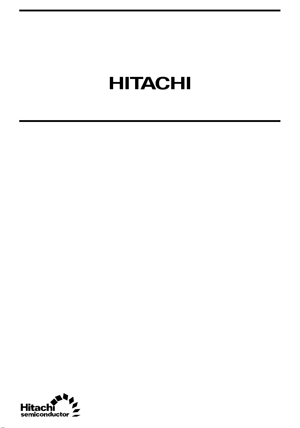
Pin Arrangement
Outputs
Inputs
Outputs
Data B
Input
QB
QA
Count
Down
Count
Up
QC
QD
GND
1
2
QB
B
A
16
15
V
CC
Data A
Inputs
3
4
5
6
7
QA
Count
Down
Count
Up
QC
Q
D
Clear
Borrow
Carry
Load
D
C
8
14
13
12
11
10
9
Clear
Borrow
Carry
Load
Data C
Data D
Outputs
Inputs
(Top view)
2
Page 3
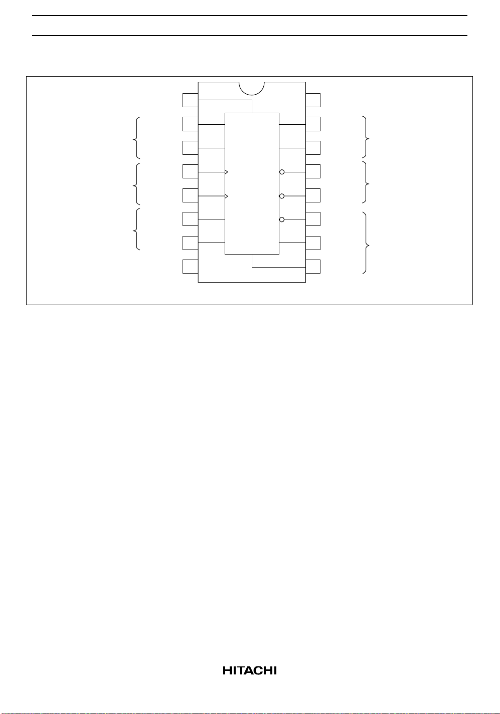
Logic Diagram
HD74HC192
Count
Down
Count
Up
Data A
Data B
Data C
HD74HC192/HD74HC193
Borrow
Carry
CK
CK
RQS
Q
QA
CK
CK
RQS
Q
QB
CK
CK
RQS
Q
QC
CK
CK
RQS
Q
QD
Data D
Load
Clear
3
Page 4
HD74HC192/HD74HC193
HD74HC193
Count
Down
Count
Up
Data A
Data B
Data C
CK
CK
RQS
CK
CK
RQS
CK
CK
RQS
CK
CK
RQS
Borrow
Carry
Q
QA
Q
QB
Q
QC
Q
QD
Data D
Load
Clear
4
Page 5

Timing Chart
HD74HC192
Illustrated below is the following sequence:
1. Clear outputs to zero.
2. Load (preset) to binary seven.
3. Count up to eight, nine, zero, one and two.
4. Count down to one, zero, borrow, nine, eight and seven.
Clear
Load
A
B
Data
Inputs
C
D
HD74HC192/HD74HC193
Count Up
Count Down
Q
Q
QC
QD
Carry
Borrow
Sequence
Illustrated
A
B
89012 10987
0
Clear
7
Preset
Count Up Count Down
5
Page 6

HD74HC192/HD74HC193
HD74HC191
Illustrated below is the following sequence:
1. Clear outputs to zero.
2. Load (preset) to binary thirteen.
3. Count up to fourteen, fifteen, zero, one and two.
4. Count down to one, zero, borrow, fifteen and thirteen.
Clear
Load
A
B
Data
Inputs
C
D
Count Up
Count Down
Outputs
Carry
Borrow
Q
Q
QC
QD
A
B
0
Clear
13
Preset
14 15 0 1 2 1 0 15 14 13
Count Up Count Down
6
Page 7

HD74HC192/HD74HC193
DC Characteristics
Ta = –40 to
Ta = 25°C
Item Symbol V
Input voltage V
IH
(V) Min Typ Max Min Max Unit Test Conditions
CC
2.0 1.5 — — 1.5 — V
4.5 3.15 — — 3.15 —
6.0 4.2 — — 4.2 —
V
IL
2.0 — — 0.5 — 0.5 V
4.5 — — 1.35 — 1.35
6.0 — — 1.8 — 1.8
Output voltage V
OH
2.0 1.9 2.0 — 1.9 — V Vin = VIH or VILIOH = –20 µA
4.5 4.4 4.5 — 4.4 —
6.0 5.9 6.0 — 5.9 —
4.5 4.18 — — 4.13 — IOH = –4 mA
6.0 5.68 — — 5.63 — IOH = –5.2 mA
V
OL
2.0 — 0.0 0.1 — 0.1 V Vin = VIH or VILIOL = 20 µA
4.5 — 0.0 0.1 — 0.1
6.0 — 0.0 0.1 — 0.1
4.5 — — 0.26 — 0.33 IOL = 4 mA
6.0 — — 0.26 — 0.33 IOL = 5.2 mA
Input current Iin 6.0 — — ±0.1 — ±1.0 µA Vin = VCC or GND
Quiescent supply
I
CC
6.0 — — 4.0 — 40 µA Vin = VCC or GND, Iout = 0 µA
current
+85°C
7
Page 8

HD74HC192/HD74HC193
AC Characteristics (CL = 50 pF, Input tr = tf = 6 ns)
Ta = –40 to
Ta = 25°C
Item Symbol V
Maximum clock f
max
(V) Min Typ Max Min Max Unit Test Conditions
CC
2.0 — — 4 — 3 MHz
frequency 4.5 — — 20 — 16
6.0 — — 24 — 19
Propagation delay t
PLH
2.0 — — 140 — 175 ns Count up to Carry
time 4.5 — 14 28 — 35
6.0 — — 24 — 30
t
PHL
2.0 — — 130 — 165
4.5 — 15 26 — 33
6.0 — — 22 — 28
t
PLH
2.0 — — 130 — 165 Count down to Borrow
4.5 — 14 26 — 33
6.0 — — 22 — 28
t
PHL
2.0 — — 130 — 165
4.5 — 15 26 — 33
6.0 — — 22 — 28
t
PLH
2.0 — — 215 — 270 Count up or down to Q
4.5 — 21 43 — 54
6.0 — — 37 — 46
t
PHL
2.0 — — 275 — 345
4.5 — 21 55 — 69
6.0 — — 47 — 59
t
PLH
2.0 — — 230 — 290 Load to Q
4.5 — 17 46 — 58
6.0 — — 39 — 49
t
PHL
2.0 — — 290 — 365
4.5 — 23 58 — 73
6.0 — — 49 — 62
t
PHL
2.0 — — 265 — 335 Clear to Q
4.5 — 24 53 — 66
6.0 — — 45 — 56
Pulse width t
w
2.0 80 — — 100 — ns
4.5 16 8 — 20 —
6.0 14 – — 17 —
+85°C
8
Page 9

HD74HC192/HD74HC193
AC Characteristics (CL = 50 pF, Input tr = tf = 6 ns) (cont)
Ta = –40 to
Ta = 25°C
Item Symbol V
Hold time t
h
(V) Min Typ Max Min Max Unit Test Conditions
CC
2.0 5 — — 5 — ns Data to Load
4.5 5 –3 — 5 —
6.0 5 — — 5 —
Setup time t
su
2.0 100 — — 125 — ns Data to Load
4.5 20 4 — 25 —
6.0 17 — — 21 —
Removal time t
rem
2.0 50 — — 65 — ns Clear to Clock
4.5 10 –1 — 13 —
6.0 9 — — 11 —
Output rise/fall t
time t
TLH
THL
2.0 — — 75 — 95 ns
4.5 — 5 15 — 19
6.0 — — 13 — 16
Input capacitance Cin — — 5 10 — 10 pF
+85°C
9
Page 10

19.20
20.00 Max
16 9
1.3
Unit: mm
6.30
7.40 Max
81
1.11 Max
2.54 ± 0.25
0.48 ± 0.10
5.06 Max
2.54 Min
0.51 Min
Hitachi Code
JEDEC
EIAJ
Weight
7.62
+ 0.13
0.25
– 0.05
0° – 15°
(reference value)
DP-16
Conforms
Conforms
1.07 g
Page 11

16
Unit: mm
10.06
10.5 Max
9
5.5
1
0.80 Max
1.27
*0.42 ± 0.08
0.40 ± 0.06
*Dimension including the plating thickness
Base material dimension
8
0.12
0.10 ± 0.10
0.15
M
2.20 Max
7.80
0.20 ± 0.04
*0.22 ± 0.05
0.70 ± 0.20
Hitachi Code
JEDEC
EIAJ
(reference value)
Weight
+ 0.20
– 0.30
1.15
0° – 8°
FP-16DA
—
Conforms
0.24 g
Page 12

16
Unit: mm
9.9
10.3 Max
9
1
1.27
0.635 Max
*0.42 ± 0.08
0.40 ± 0.06
*Dimension including the plating thickness
Base material dimension
8
0.25
+ 0.11
– 0.04
0.14
0.15
3.95
1.75 Max
M
6.10
1.08
0.20 ± 0.03
*0.22 ± 0.03
0.60
Hitachi Code
JEDEC
EIAJ
Weight
+ 0.10
– 0.30
0° – 8°
+ 0.67
– 0.20
(reference value)
FP-16DN
Conforms
Conforms
0.15 g
Page 13

Cautions
1. Hitachi neither warrants nor grants licenses of any rights of Hitachi’s or any third party’s patent,
copyright, trademark, or other intellectual property rights for information contained in this document.
Hitachi bears no responsibility for problems that may arise with third party’s rights, including
intellectual property rights, in connection with use of the information contained in this document.
2. Products and product specifications may be subject to change without notice. Confirm that you have
received the latest product standards or specifications before final design, purchase or use.
3. Hitachi makes every attempt to ensure that its products are of high quality and reliability. However,
contact Hitachi’s sales office before using the product in an application that demands especially high
quality and reliability or where its failure or malfunction may directly threaten human life or cause risk
of bodily injury, such as aerospace, aeronautics, nuclear power, combustion control, transportation,
traffic, safety equipment or medical equipment for life support.
4. Design your application so that the product is used within the ranges guaranteed by Hitachi particularly
for maximum rating, operating supply voltage range, heat radiation characteristics, installation
conditions and other characteristics. Hitachi bears no responsibility for failure or damage when used
beyond the guaranteed ranges. Even within the guaranteed ranges, consider normally foreseeable
failure rates or failure modes in semiconductor devices and employ systemic measures such as failsafes, so that the equipment incorporating Hitachi product does not cause bodily injury, fire or other
consequential damage due to operation of the Hitachi product.
5. This product is not designed to be radiation resistant.
6. No one is permitted to reproduce or duplicate, in any form, the whole or part of this document without
written approval from Hitachi.
7. Contact Hitachi’s sales office for any questions regarding this document or Hitachi semiconductor
products.
Hitachi, Ltd.
Semiconductor & Integrated Circuits.
Nippon Bldg., 2-6-2, Ohte-machi, Chiyoda-ku, Tokyo 100-0004, Japan
Tel: Tokyo (03) 3270-2111 Fax: (03) 3270-5109
URL NorthAmerica : http:semiconductor.hitachi.com/
For further information write to:
Hitachi Semiconductor
(America) Inc.
179 East Tasman Drive,
San Jose,CA 95134
Tel: <1> (408) 433-1990
Fax: <1>(408) 433-0223
Europe : http://www.hitachi-eu.com/hel/ecg
Asia (Singapore) : http://www.has.hitachi.com.sg/grp3/sicd/index.htm
Asia (Taiwan) : http://www.hitachi.com.tw/E/Product/SICD_Frame.htm
Asia (HongKong) : http://www.hitachi.com.hk/eng/bo/grp3/index.htm
Japan : http://www.hitachi.co.jp/Sicd/indx.htm
Hitachi Europe GmbH
Electronic components Group
Dornacher Stra§e 3
D-85622 Feldkirchen, Munich
Germany
Tel: <49> (89) 9 9180-0
Fax: <49> (89) 9 29 30 00
Hitachi Europe Ltd.
Electronic Components Group.
Whitebrook Park
Lower Cookham Road
Maidenhead
Berkshire SL6 8YA, United Kingdom
Tel: <44> (1628) 585000
Fax: <44> (1628) 778322
Hitachi Asia Pte. Ltd.
16 Collyer Quay #20-00
Hitachi Tower
Singapore 049318
Tel: 535-2100
Fax: 535-1533
Hitachi Asia Ltd.
Taipei Branch Office
3F, Hung Kuo Building. No.167,
Tun-Hwa North Road, Taipei (105)
Tel: <886> (2) 2718-3666
Fax: <886> (2) 2718-8180
Copyright ' Hitachi, Ltd., 1999. All rights reserved. Printed in Japan.
Hitachi Asia (Hong Kong) Ltd.
Group III (Electronic Components)
7/F., North Tower, World Finance Centre,
Harbour City, Canton Road, Tsim Sha Tsui,
Kowloon, Hong Kong
Tel: <852> (2) 735 9218
Fax: <852> (2) 730 0281
Telex: 40815 HITEC HX
 Loading...