

Page 1
HD74HC123A
Dual Retriggerable Monostable Multivibrators (with Clear)
Description
This multivibrator features both a negative, A, and a positive, B, transition triggered input, either of which
can be used as an inhibit input. Also included is a clear input that when taken low resets the one shot. The
HD74HC123A can be triggered on the positive transition of the clear while A is held low and B is held
high.
The HD74HC123A is retriggerable. That is it may be triggered repeatedly while their outputs are
generating a pulse and the pulse will be extended.
Pulse width stability over a wide range of temperature. The output pulse equation is simply: tw = (Rext)
(Cext).
Features
• High Speed Operation
• High Output Current: Fanout of 10 LSTTL Loads
• Wide Operating Voltage: VCC = 2 to 6 V
• Low Input Current: 1 µA max
• Low Quiescent Supply Current
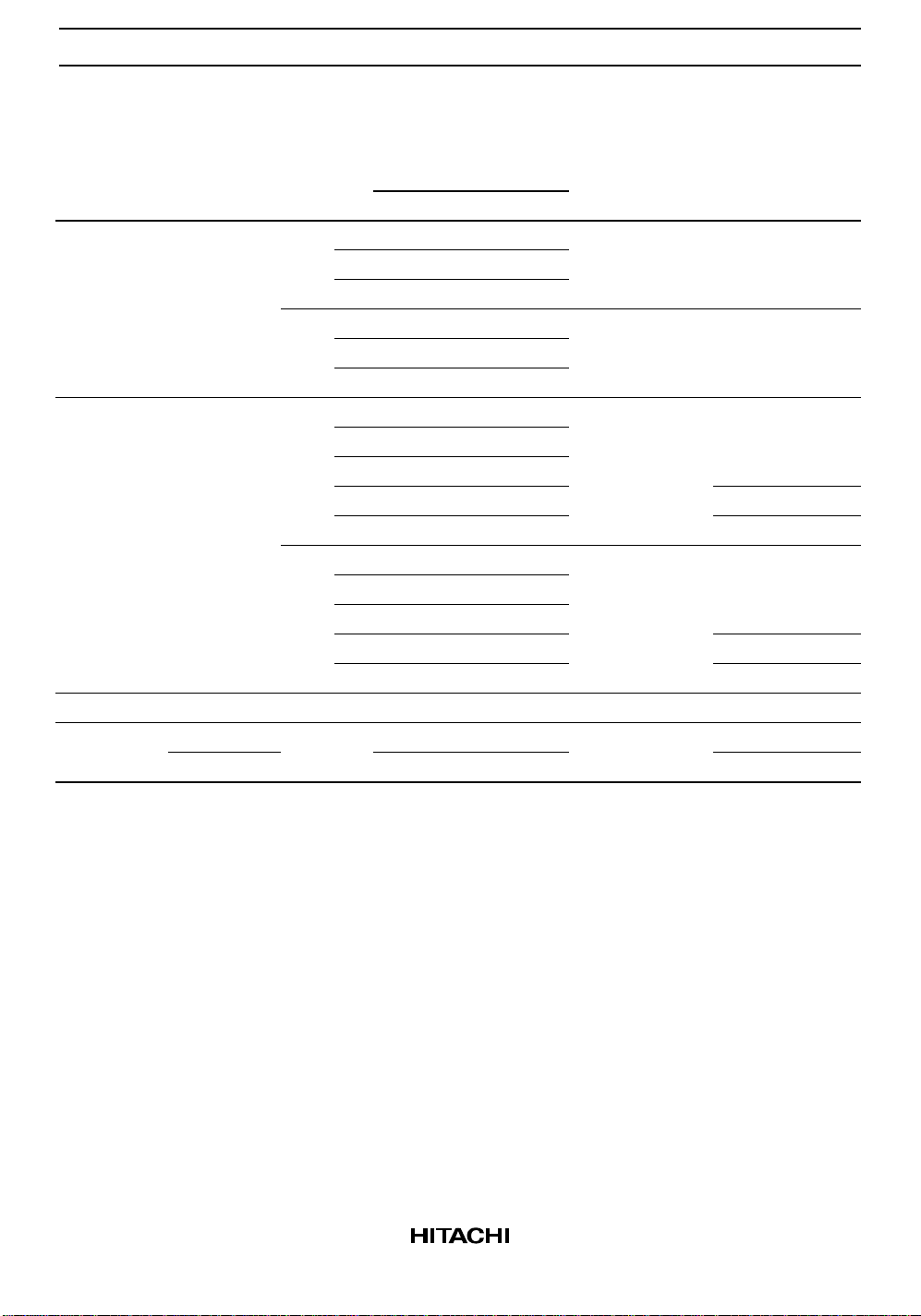
Function Table
Inputs Outputs
Clear A B Q Q
LXXLH
XHXLH
XX L L H
HL
H H
LH
Note: External timing capacitance connects between Cext and Rext/Cext.
Page 2
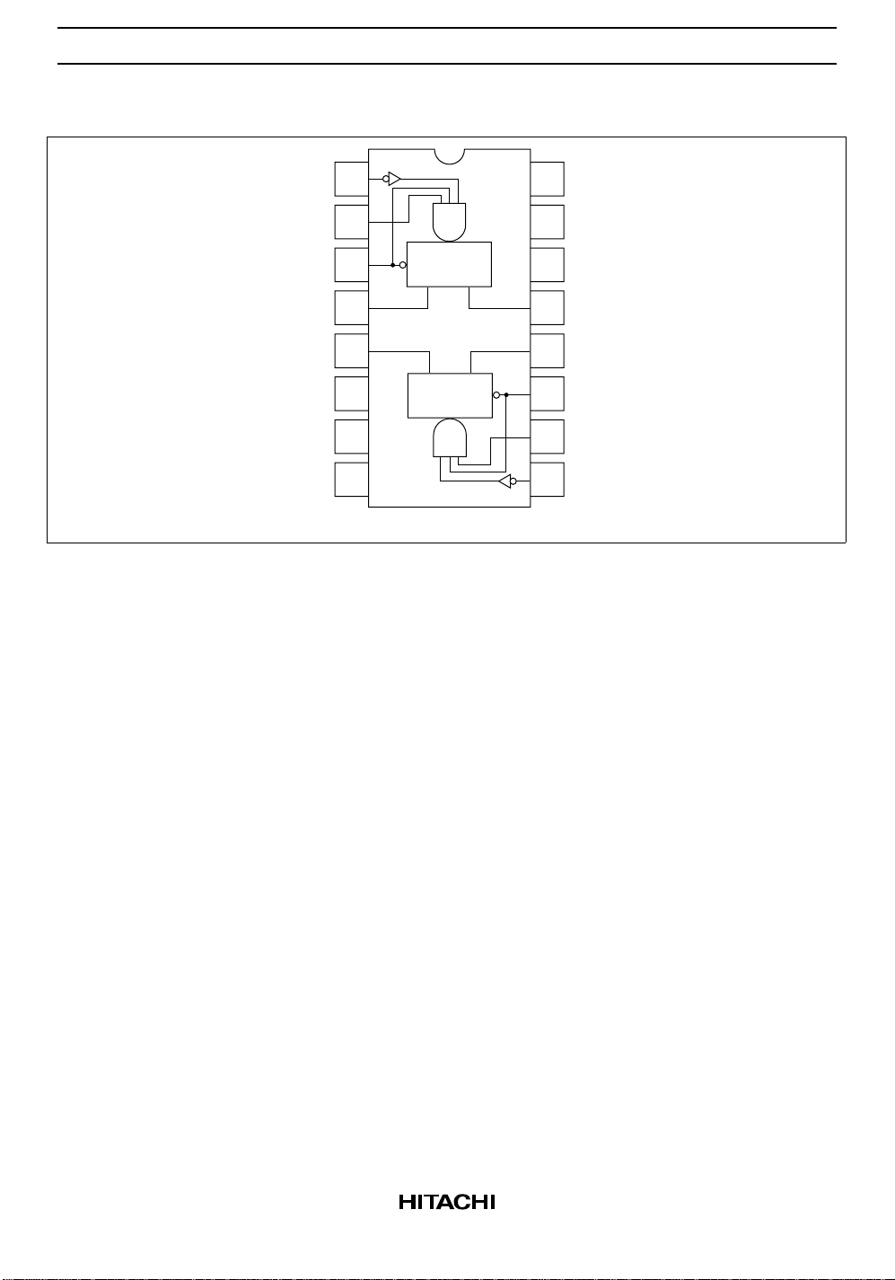
HD74HC123A
Pin Arrangement
1A
2Rext/
Cext
1
21B
31CLR
41Q
52Q
62Cext
7
8GND
CLR
Q Q
QQ
CLR
(Top view)
16
15
V
CC
1Rext
Cext
1Cext14
1Q13
2Q12
2CLR11
2B10
2A9
2
Page 3
HD74HC123A
DC Characteristics
Ta = –40
Sym- VCCTa = 25°C
Item bol (V) Min Typ Max Min Max Unit Test Conditions
Input voltage V
2.0 1.5 — — 1.5 — V
IH
4.5 3.15 — — 3.15 —
6.0 4.2 — — 4.2 —
V
2.0 — — 0.5 — 0.5 V
IL
4.5 — — 1.35 — 1.35
6.0 — — 1.8 — 1.8
Output voltage V
2.0 1.9 2.0 — 1.9 — V Vin = VIH or VILIOH = –20 µA
OH
4.5 4.4 4.5 — 4.4 —
6.0 5.9 6.0 — 5.9 —
4.5 4.18 — — 4.13 — IOH = –4 mA
6.0 5.68 — — 5.63 — IOH = –5.2 mA
V
2.0 — 0.0 0.1 — 0.1 V Vin = VIH or VILIOL = 20 µA
OL
4.5 — 0.0 0.1 — 0.1
6.0 — 0.0 0.1 — 0.1
4.5 — — 0.26 — 0.33 IOL = 4 mA
6.0 — — 0.26 — 0.33 IOL = 5.2 mA
Input current Iin 6.0 — — ±0.1 — ±1.0 µA Vin = VCC or GND
Quiescent Standby state I
6.0 — — 130 — 220 µA Vin = VCC or Iout = 0 µA
CC
supply current Active state — — 130 — 220 GND Rext/Cext = 0.5 V
to +85°C
CC
3
Page 4

HD74HC123A
AC Characteristics (CL = 50 pF, Input tr = tf = 6 ns)
Ta = –40 to
Ta = 25°C
Item Symbol V
Propagation delay t
PLH
(V) Min Typ Max Min Max Unit Test Conditions
CC
2.0 — — 210 — 265 ns A, B or Clear to Q
time 4.5 — 22 42 — 53
6.0 — — 36 — 45
t
PHL
2.0 — — 240 — 300 ns A, B or Clear to Q
4.5 — 23 48 — 60
6.0 — — 41 — 51
t
PHL
2.0 — — 170 — 215 ns Clear to Q
4.5 — 18 34 — 43
6.0 — — 29 — 37
t
PLH
2.0 — — 180 — 225 ns Clear to Q
4.5 — 16 36 — 45
6.0 — — 31 — 38
Output rise time t
TLH
2.0 — — 75 — 95 ns
4.5 — 5 15 — 19
6.0 — — 13 — 16
Output fall time t
THL
2.0 — — 75 — 95 ns
4.5 — 5 15 — 19
6.0 — — 13 — 16
Pulse width t
w
2.0 150 — — 190 — ns A, B, Clear
4.5 30 6 — 38 —
6.0 26 — — 33 —
Minimum output t
WQ(min)
2.0 — 1.5 — — — µs Cext = 28 pF Rext = 6 kΩ
pulse width 4.5 — 450 — — — ns Rext = 2 kΩ
6.0 — 380 — — —
Output pulse width t
WQ
4.5 — 1.0 — — — ms Cext = 0.1 µF, Rext = 10 kΩ
Input capacitance Cin — — 5 10 — 10 pF
Caution in use: In order to prevent any malfunctions due to noise, connect a high-frequency performance
capacitor between V
and GND, and keep the wiring between the External components
CC
and Cext, Rext/Cext pins as short as possible.
+85°C
4
Page 5

19.20
20.00 Max
16 9
1.3
Unit: mm
6.30
7.40 Max
81
1.11 Max
2.54 ± 0.25
0.48 ± 0.10
5.06 Max
2.54 Min
0.51 Min
Hitachi Code
JEDEC
EIAJ
Weight
7.62
+ 0.13
0.25
– 0.05
0° – 15°
(reference value)
DP-16
Conforms
Conforms
1.07 g
Page 6

16
Unit: mm
10.06
10.5 Max
9
5.5
1
0.80 Max
1.27
*0.42 ± 0.08
0.40 ± 0.06
*Dimension including the plating thickness
Base material dimension
8
0.12
0.10 ± 0.10
0.15
M
2.20 Max
7.80
0.20 ± 0.04
*0.22 ± 0.05
0.70 ± 0.20
Hitachi Code
JEDEC
EIAJ
(reference value)
Weight
+ 0.20
– 0.30
1.15
0° – 8°
FP-16DA
—
Conforms
0.24 g
Page 7

16
Unit: mm
9.9
10.3 Max
9
1
1.27
0.635 Max
*0.42 ± 0.08
0.40 ± 0.06
*Dimension including the plating thickness
Base material dimension
8
0.25
+ 0.11
– 0.04
0.14
0.15
3.95
1.75 Max
M
6.10
1.08
0.20 ± 0.03
*0.22 ± 0.03
0.60
Hitachi Code
JEDEC
EIAJ
Weight
+ 0.10
– 0.30
0° – 8°
+ 0.67
– 0.20
(reference value)
FP-16DN
Conforms
Conforms
0.15 g
Page 8

Cautions
1. Hitachi neither warrants nor grants licenses of any rights of Hitachi’s or any third party’s patent,
copyright, trademark, or other intellectual property rights for information contained in this document.
Hitachi bears no responsibility for problems that may arise with third party’s rights, including
intellectual property rights, in connection with use of the information contained in this document.
2. Products and product specifications may be subject to change without notice. Confirm that you have
received the latest product standards or specifications before final design, purchase or use.
3. Hitachi makes every attempt to ensure that its products are of high quality and reliability. However,
contact Hitachi’s sales office before using the product in an application that demands especially high
quality and reliability or where its failure or malfunction may directly threaten human life or cause risk
of bodily injury, such as aerospace, aeronautics, nuclear power, combustion control, transportation,
traffic, safety equipment or medical equipment for life support.
4. Design your application so that the product is used within the ranges guaranteed by Hitachi particularly
for maximum rating, operating supply voltage range, heat radiation characteristics, installation
conditions and other characteristics. Hitachi bears no responsibility for failure or damage when used
beyond the guaranteed ranges. Even within the guaranteed ranges, consider normally foreseeable
failure rates or failure modes in semiconductor devices and employ systemic measures such as failsafes, so that the equipment incorporating Hitachi product does not cause bodily injury, fire or other
consequential damage due to operation of the Hitachi product.
5. This product is not designed to be radiation resistant.
6. No one is permitted to reproduce or duplicate, in any form, the whole or part of this document without
written approval from Hitachi.
7. Contact Hitachi’s sales office for any questions regarding this document or Hitachi semiconductor
products.
Hitachi, Ltd.
Semiconductor & Integrated Circuits.
Nippon Bldg., 2-6-2, Ohte-machi, Chiyoda-ku, Tokyo 100-0004, Japan
Tel: Tokyo (03) 3270-2111 Fax: (03) 3270-5109
URL NorthAmerica : http:semiconductor.hitachi.com/
For further information write to:
Hitachi Semiconductor
(America) Inc.
179 East Tasman Drive,
San Jose,CA 95134
Tel: <1> (408) 433-1990
Fax: <1>(408) 433-0223
Europe : http://www.hitachi-eu.com/hel/ecg
Asia (Singapore) : http://www.has.hitachi.com.sg/grp3/sicd/index.htm
Asia (Taiwan) : http://www.hitachi.com.tw/E/Product/SICD_Frame.htm
Asia (HongKong) : http://www.hitachi.com.hk/eng/bo/grp3/index.htm
Japan : http://www.hitachi.co.jp/Sicd/indx.htm
Hitachi Europe GmbH
Electronic components Group
Dornacher Stra§e 3
D-85622 Feldkirchen, Munich
Germany
Tel: <49> (89) 9 9180-0
Fax: <49> (89) 9 29 30 00
Hitachi Europe Ltd.
Electronic Components Group.
Whitebrook Park
Lower Cookham Road
Maidenhead
Berkshire SL6 8YA, United Kingdom
Tel: <44> (1628) 585000
Fax: <44> (1628) 778322
Hitachi Asia Pte. Ltd.
16 Collyer Quay #20-00
Hitachi Tower
Singapore 049318
Tel: 535-2100
Fax: 535-1533
Hitachi Asia Ltd.
Taipei Branch Office
3F, Hung Kuo Building. No.167,
Tun-Hwa North Road, Taipei (105)
Tel: <886> (2) 2718-3666
Fax: <886> (2) 2718-8180
Copyright ' Hitachi, Ltd., 1999. All rights reserved. Printed in Japan.
Hitachi Asia (Hong Kong) Ltd.
Group III (Electronic Components)
7/F., North Tower, World Finance Centre,
Harbour City, Canton Road, Tsim Sha Tsui,
Kowloon, Hong Kong
Tel: <852> (2) 735 9218
Fax: <852> (2) 730 0281
Telex: 40815 HITEC HX
 Loading...