

Page 1

HD74CDCV857
2.5-V Phase-lock Loop Clock Driver
ADE-205-335C (Z)
Preliminary
4th Edition
March 2000
Description
The HD74CDCV857 is a high-performance, low-skew, low-jitter, phase locked loop clock driver. It is
specifically designed for use with DDR (Double Data Rate) synchronous DRAMs.
Features
• Supports 60 MHz to 200 MHz operation range
• Distributes one differential clock input pair to ten differential clock outputs pairs
• Supports spread spectrum clock requirements meeting the PC100 SDRAM registered DIMM
specification
• External feedback pins (FBIN, FBIN) are used to synchronize the outputs to the clock input
• Supports 2.5V analog supply voltage (AVCC), and 2.5 V V
• No external RC network required
• Sleep mode detection
• 48pin TSSOP (Thin Shrink Small Outline Package)
DDQ
Page 2

HD74CDCV857
Function Table
Inputs : Outputs : PLL
AV
GND H L H : L H L H : Bypassed / off
GND H H L : H L H L : Bypassed / off
XL LH: ZZZZ:off
XL HL: ZZZZ:off
2.5 V H L H : HL HL:on
2.5 V H H L : HL HL:on
2.5 V X 0 MHz 0 MHz : ZZZZ:off
H : High level
L : Low level
X : Don’t care
Z : High impedance
Note: 1. Bypasse mode is used for Hitachi test mode.
PWRDWN CLK CLK : Y Y FBOUT FBOUT
CC
*1
*1
2
Page 3
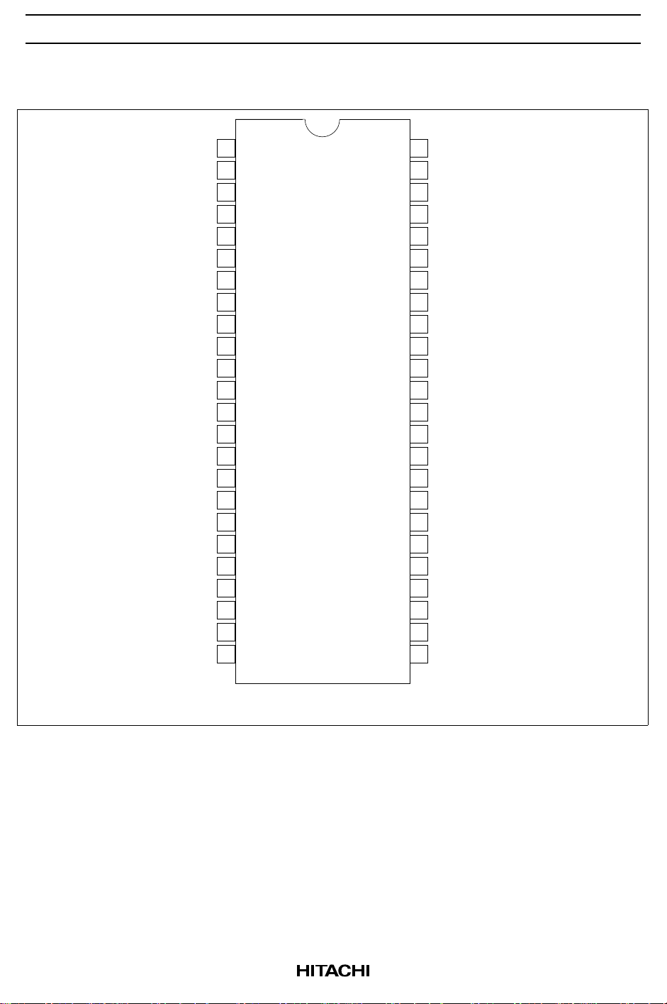
Pin Arrangement
N
GND
Y0
Y0
V
DDQ
Y1
Y1
GND
GND
Y2
Y2
V
DDQ
V
DDQ
CLK
CLK
V
DDQ
AV
CC
AGND
GND
Y3
Y3
V
DDQ
Y4
Y4
GND
10
11
12
13
14
15
16
17
18
19
20
21
22
23
24
HD74CDCV857
GND
1
2
3
4
5
6
7
8
9
48
47
46
45
44
43
42
41
40
39
38
37
36
35
34
33
32
31
30
29
28
27
26
25
Y5
Y5
V
DDQ
Y6
Y6
GND
GND
Y7
Y7
V
DDQ
PWRDW
FBIN
FBIN
V
DDQ
FBOUT
FBOUT
GND
Y8
Y8
V
DDQ
Y9
Y9
GND
(Top view)
3
Page 4

HD74CDCV857
CC
CC
Pin Function
Pin name No. Type Description
AGND 17 Ground Analog ground. AGND provides the ground reference for the
analog circuitry.
AV
CC
CLK, CLK 13, 14 I
FBIN, FBIN 35, 36 I
FBOUT, FBOUT 32, 33 O
PWRDWN 37 I Output bank enable. PWRDWN is the output enable for all
GND 1, 7, 8, 18,
V
DDQ
Y 3, 5, 10, 20,
Y 2, 6, 9, 19,
16 Power Analog power supply. AVCC provides the power reference for
the analog circuitry. In addition, AV
the PLL for test purposes. When AV
can be used to bypass
is strapped to ground,
PLL is bypassed and CLK is buffered directly to the device
outputs. This bypass mode is used for Hitachi test.
Clock input. CLK provides the clock signal to be distributed by
Differential
input
the HD74CDCV857 clock driver. CLK is used to provide the
reference signal to the integrated PLL that generates the clock
output signals. CLK must have a fixed frequency and fixed
phase for the PLL to obtain phase lock. Once the circuit is
powered up and a valid CLK signal is applied, a stabilization
time is required for the PLL to phase lock the feedback signal to
its reference signal.
Feedback input. FBIN provides the feedback signal to the
Differential
input
internal PLL. FBIN must be hard-wired to FBOUT to complete
the PLL. The integrated PLL synchronizes CLK and FBIN so
that there is nominally zero phase error between CLK and
FBIN.
Feedback output. FBOUT is dedicated for external feedback. It
Differential
output
switches at the same frequency as CLK. When externally wired
to FBIN, FBOUT completes the feedback loop of the PLL.
outputs. When PWRDWN is low, VCO will stop and all outputs
are disabled to a high impedance state. When PWRDWN will
be returned high, PLL will re-synchroniz to CLK frequency and
all outputs are enabled.
Ground Ground
24, 25, 31,
41, 42, 48
4, 11, 12,
Power Power supply
15, 21, 28,
34, 38, 45
22, 27, 29,
39, 44, 46
23, 26, 30,
40, 43, 47
O
Differential
output
O
Differential
output
Clock outputs. These outputs provide low-skew copies of CLK.
Clock outputs. These outputs provide low-skew copies of CLK.
4
Page 5
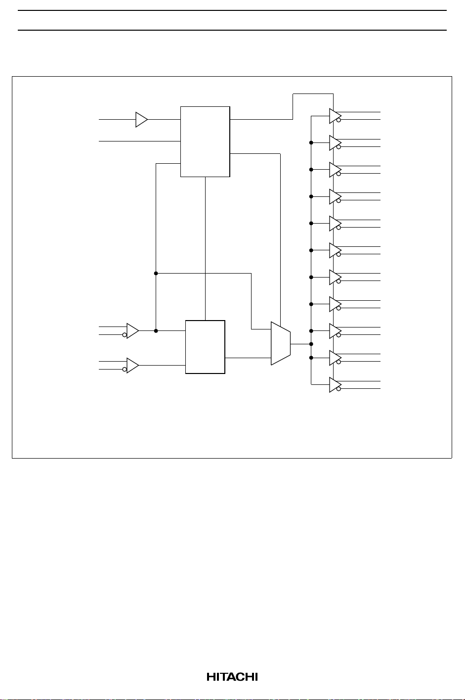
Logic Diagram
PWRDWN
AV
CC
CLK
CLK
FBIN
FBIN
HD74CDCV857
3
Y0
37
16
Powerdown
and Test
Logic
13
14
PLL
36
35
2
5
6
10
9
20
19
22
23
46
47
44
43
39
40
29
30
27
26
32
33
Y0
Y1
Y1
Y2
Y2
Y3
Y3
Y4
Y4
Y5
Y5
Y6
Y6
Y7
Y7
Y8
Y8
Y9
Y9
FBOUT
FBOUT
Note: All inputs and outputs are associated with V = 2.5 V.
DDQ
5
Page 6

HD74CDCV857
Q
Absolute Maximum Ratings
Item Symbol Ratings Unit Conditions
Supply voltage V
Input voltage V
Output voltage
*1
Input clamp current I
Output clamp current I
Continuous output current I
Supply current through each V
or GND I
DDQ
V
IK
OK
O
VDDQ
DDQ
I
O
or I
GND
Maximum power dissipation
at Ta = 55°C (in still air)
Storage temperature T
stg
Notes: Stresses beyond those listed under “absolute maximum ratings” may cause permanent damage
to the device. These are stress ratings only, and functional operation of the device at these or
any other conditions beyond those indicated under “recommended operating conditions” is not
implied. Exposure to absolute maximum rated conditions for extended periods may affect device
reliability.
1. The input and output negative voltage ratings may be exceeded if the input and output clamp
current ratings are observed.
–0.5 to 3.6 V
–0.5 to V
–0.5 to V
DDQ
DD
+0.5 V
V
+0.5
–50 mA VI < 0
–50 mA VO < 0
±50 mA VO = 0 to V
±100 mA
0.7 W
–65 to +150 °C
DDQ
6
Page 7

HD74CDCV857
Q
Q
Recommended Operating Conditions
Item Symbol Min Typ Max Unit Conditions
Supply voltage AV
Output supply voltage V
DC input signal voltage
*1
High level input voltage V
Low level input voltage V
Differential input signal voltage *2V
Differential cross point voltage *3V
Output current I
DDQ
IHG
ILG
ID
IX
V
OX
OH
I
OL
Input slew rate SR 1 — 4 V/ns 20% – 80%
Operating temperature T
a
Notes: Inputs pins must be prevent from floating.
Feedback inputs (FBIN, FBIN) may float when the device is in low power mode.
1. DC input signal voltage specifies the allowable dc execution of differential input.
2. Differential cross point voltage is expected to track variations of V
the differential signals must be crossing. (See figure1-1)
2.3 2.5 2.7 V
CC
2.3 2.5 2.7 V
–0.3 — V
1.7 — V
+0.3 V All pins
DDQ
+0.3 V PWRDWN input pin
DDQ
–0.3 — 0.7 V PWRDWN input pin
0.36 — V
0.5×V
— 0.5×V
DD
–0.20
DDQ
+0.20
+0.6 V
DD
V
— — –12 mA
——12
0—70°C
and is the voltage at which
DDQ
CLK
CLK
V
ID
Crossing point
Figure 1 Differential input levels
7
Page 8

HD74CDCV857
Electrical Characteristics
Item Symbol Min Typ *1Max Unit Test Conditions
Input clamp
voltage
CLK, CLK
FBIN, FBIN, G
Output voltage V
Input current I
Input capacitance C
Delta input capacitance C
Supply current DI
Supply current in power
down mode
Note: 1. For conditions shown as Min or Max, use the appropriate value specified under recommended
operating conditions.
V
V
AI
I
IK
OH
OL
I
I
DI
CCpd
— — –1.2 V II = –18 mA, V
= 2.3 V
DDQ
VCC–0.2 — — V IOH = –100 µA, VCC = 2.3 to 2.7 V
1.7 — — IOH = –12 mA, VCC = 2.3 V
— — 0.2 IOL = 100 µA, VCC = 2.3 to 2.7 V
— — 0.6 IOL = 12 mA, VCC = 2.3 V
——±10 µAVI = 0 V to 2.7 V, V
= 2.7 V
DDQ
2.5 — 3.5 pF CLK and CLK, FBIN and FBIN
–0.25 — 0.25 pF CLK and CLK, FBIN and FBIN
CC
CC
— 250 TBD mA
— 9 TBD
— — 100 µA
8
Page 9

HD74CDCV857
Switching Characteristics
Item Symbol Min Typ Max Unit Test Conditions Notes
Period jitter t
Half period jitter t
Cycle to cycle jitter t
Static phase error t
Output clock skew t
Operating clock frequency f
Application clock
PER
HPER
CC
SPE
sk
CLK(O)
f
CLK(A)
frequency
Slew rate t
PLL stabilization time t
SL
STAB
Notes: 1. The PLL must be able to handle spread spectrum induced skew (the specification for this
frequency modulation can be found in the latest Intel PC100 Registered DIMM specification)
2. Operating clock frequency indicates a range over which the PLL must be able to lock, but in
which it is not required to meet the other timing parameters.
3. Application clock frequency indicates a range over which the PLL must meet all timing
parameters.
4 Assumes equal wire length and loading on the clock output and feedback path.
5. Static phase error does not include jitter.
6. Stabilization time is the time required for the integrated PLL circuit to obtain phase lock of its
feedback signal to its reference signal after power up.
7. Period jitter defines the largest variation in clock period, around anominal clock period.
8. Period jitter and half period jitter are independent from each other.
–75 — 75 ps See figure 6, 9 7, 8
–100 — 100 ps See figure 7, 9 8
–75 — 75 ps See figure 5, 9
–50 — 50 ps See figure 3, 9 4, 5
— — 100 ps See figure 4, 9
60 — 200 MHz See figure 9 1, 2
95 133 170 MHz See figure 9 1, 3
1.0 — 2.0 V/ns See figure 9 20% – 80%
— — 0.1 ms See figure 9 6
9
Page 10

HD74CDCV857
Differential clock outputs are directly terminated by a 120 Ω resistor. Figure 2 is typical usage conditions
of outputs load.
Device
under
test
V
DDQ
OUT
OUT
V
DDQ
R =
T
120 Ω
Figure 2 Differential signal using direct termination resistor
CLKIN
CLKIN
FBIN
FBIN
t
SPE
C = 14 pF
C = 14 pF
Figure 3 Static phase error
10
Page 11

FBOUT
FBOUT
Yx
HD74CDCV857
Yx
Yx
Yx
Yx'
Yx'
t
sk
t
sk
Figure 4 Output skew
11
Page 12

HD74CDCV857
Yx, FBOUT
Yx, FBOUT
Yx, FBOUT
Yx, FBOUT
Yx, FBOUT
Yx, FBOUT
t
cycle n
t = t – t
cc cycle n cycle n+1
Figure 5 Cycle to cycle jitter
t
cycle n
1
f
o
t = t –
PER cycle n
1
f
o
t
cycle n+1
Yx, FBOUT
Yx, FBOUT
Yx, FBOUT
Yx, FBOUT
Figure 6 Period jitter
t
half period n
1
f
o
t = t –
half period nHPER
Figure 7 Half period jitter
t
half period n+1
1
2*f
o
12
Page 13

Yx, FBOUT
HD74CDCV857
Device
under
test
Device
under
test
Yx, FBOUT
V
DDQ
AV
CC
OUT
OUT
AGND
GND
V
DDQ
AV
CC
OUT
V /2
DDQ
AV /2
CC
Z = 60 Ω
Z = 60 Ω
–V /2
DDQ
V
DDQ
AV
CC
t
half cycle n
t = t – t
HCC
half cycle n half cycle n+1
Figure 8 Half cycle to cycle jitter
R =
T
10 Ω
C =
14 pF
R =
T
10 Ω
R =
T
120 Ω
Z = 60 Ω
–V /2
DDQ
–V /2
DDQ
C =
14 pF
t
half cycle n+1
Z = 50 Ω
Z = 50 Ω
C =
14 pF
Oscillo
scope
R =
T
50 Ω
R =
T
50 Ω
OUT
AGND
GND
Z = 60 Ω
C =
14 pF
Figure 9 Output load test circuit
13
Page 14

HD74CDCV857
Package Dimensions
12.50
+0.3
–0.1
Unit : mm
2548
+0.3
–0.1
6.10
124
+0.1
0.20
–0.05
0.50
0.08
M
0.65 Max
0.10
0.05 Min
1.20 max
8.10 ± 0.3
0.15 ± 0.05
Hitachi code
EIAJ code
JEDEC code
10° Max
0.50 ± 0.1
TTP-48DC
—
—
14
Page 15

HD74CDCV857
Cautions
1. Hitachi neither warrants nor grants licenses of any rights of Hitachi’s or any third party’s patent,
copyright, trademark, or other intellectual property rights for information contained in this document.
Hitachi bears no responsibility for problems that may arise with third party’s rights, including
intellectual property rights, in connection with use of the information contained in this document.
2. Products and product specifications may be subject to change without notice. Confirm that you have
received the latest product standards or specifications before final design, purchase or use.
3. Hitachi makes every attempt to ensure that its products are of high quality and reliability. However,
contact Hitachi’s sales office before using the product in an application that demands especially high
quality and reliability or where its failure or malfunction may directly threaten human life or cause risk
of bodily injury, such as aerospace, aeronautics, nuclear power, combustion control, transportation,
traffic, safety equipment or medical equipment for life support.
4. Design your application so that the product is used within the ranges guaranteed by Hitachi particularly
for maximum rating, operating supply voltage range, heat radiation characteristics, installation
conditions and other characteristics. Hitachi bears no responsibility for failure or damage when used
beyond the guaranteed ranges. Even within the guaranteed ranges, consider normally foreseeable
failure rates or failure modes in semiconductor devices and employ systemic measures such as failsafes, so that the equipment incorporating Hitachi product does not cause bodily injury, fire or other
consequential damage due to operation of the Hitachi product.
5. This product is not designed to be radiation resistant.
6. No one is permitted to reproduce or duplicate, in any form, the whole or part of this document without
written approval from Hitachi.
7. Contact Hitachi’s sales office for any questions regarding this document or Hitachi semiconductor
products.
Hitachi, Ltd.
Semiconductor & Integrated Circuits.
Nippon Bldg., 2-6-2, Ohte-machi, Chiyoda-ku, Tokyo 100-0004, Japan
Tel: Tokyo (03) 3270-2111 Fax: (03) 3270-5109
URL NorthAmerica : http:semiconductor.hitachi.com/
For further information write to:
Hitachi Semiconductor
(America) Inc.
179 East Tasman Drive,
San Jose,CA 95134
Tel: <1> (408) 433-1990
Fax: <1>(408) 433-0223
Europe : http://www.hitachi-eu.com/hel/ecg
Asia (Singapore) : http://www.has.hitachi.com.sg/grp3/sicd/index.htm
Asia (Taiwan) : http://www.hitachi.com.tw/E/Product/SICD_Frame.htm
Asia (HongKong) : http://www.hitachi.com.hk/eng/bo/grp3/index.htm
Japan : http://www.hitachi.co.jp/Sicd/index.htm
Hitachi Europe GmbH
Electronic components Group
Dornacher Stra§e 3
D-85622 Feldkirchen, Munich
Germany
Tel: <49> (89) 9 9180-0
Fax: <49> (89) 9 29 30 00
Hitachi Europe Ltd.
Electronic Components Group.
Whitebrook Park
Lower Cookham Road
Maidenhead
Berkshire SL6 8YA, United Kingdom
Tel: <44> (1628) 585000
Fax: <44> (1628) 778322
Hitachi Asia Pte. Ltd.
16 Collyer Quay #20-00
Hitachi Tower
Singapore 049318
Tel: 535-2100
Fax: 535-1533
Hitachi Asia Ltd.
Taipei Branch Office
3F, Hung Kuo Building. No.167,
Tun-Hwa North Road, Taipei (105)
Tel: <886> (2) 2718-3666
Fax: <886> (2) 2718-8180
Copyright ' Hitachi, Ltd., 2000. All rights reserved. Printed in Japan.
Hitachi Asia (Hong Kong) Ltd.
Group III (Electronic Components)
7/F., North Tower, World Finance Centre,
Harbour City, Canton Road, Tsim Sha Tsui,
Kowloon, Hong Kong
Tel: <852> (2) 735 9218
Fax: <852> (2) 730 0281
Telex: 40815 HITEC HX
15
 Loading...