

Page 1

HD74CDCF2510B
140 MHz, 0 to 85°C Operation
3.3-V Phase-lock Loop Clock Driver
ADE-205-225F (Z)
7th. Edition
January 2000
Description
The HD74CDCF2510B is a high-performance, low-skew, low-jitter, phase-lock loop clock driver. It uses a
phase-lock loop (PLL) to precisely align, in both frequency and phase, the feedback (FBOUT) output to the
clock (CLK) input signal. It is specifically designed for use with synchronous DRAMs. The
HD74CDCF2510B operates at 3.3 V VCC and is designed to drive up to five clock loads per output.
Bank of outputs provide ten low-skew, low-jitter copies of the input clock. Output signal duty cycles are
adjusted to 50 percent independent of the duty cycle at the input clock. Bank of outputs can be enabled or
disabled via the control (G) inputs. When the G inputs are high, the outputs switch in phase and frequency
with CLK; when the G inputs are low, the outputs are disabled to the logic-low state.
Unlike many products containing PLLs, the HD74CDCF2510B does not require external RC networks.
The loop filter for the PLL is included on-chip, minimizing component count, board space, and cost.
Because it is based on PLL circuitry, HD74CDCF2510B requires a stabilization time to achieve phase lock
of the feedback signal to the reference signal. This stabilization time is required, following power up and
application of a fixed-frequency, fixed-phase signal at CLK, as well as following any changes to the PLL
reference or feedback signals. The PLL can be bypassed for test purposes by strapping AVCC to ground.
Features
• Supports PC133 and meets “PC SDRAM registered DIMM specification, Rev. 1.1”
• Phase-lock loop clock distribution for synchronous DRAM applications
• External feedback (FBIN) pin is used to synchronize the outputs to the clock input
• No external RC network required
• Support spread spectrum clock (SSC) synthesizers
• Supports frequencies up to 140 MHz
• 0 to 85°C operating range
Page 2
HD74CDCF2510B
Function Table
Inputs Outputs
G CLK 1Y (0:9) FBOUT
XLLL
LHLH
HHHH
H : High level
L : Low level
X : Immaterial
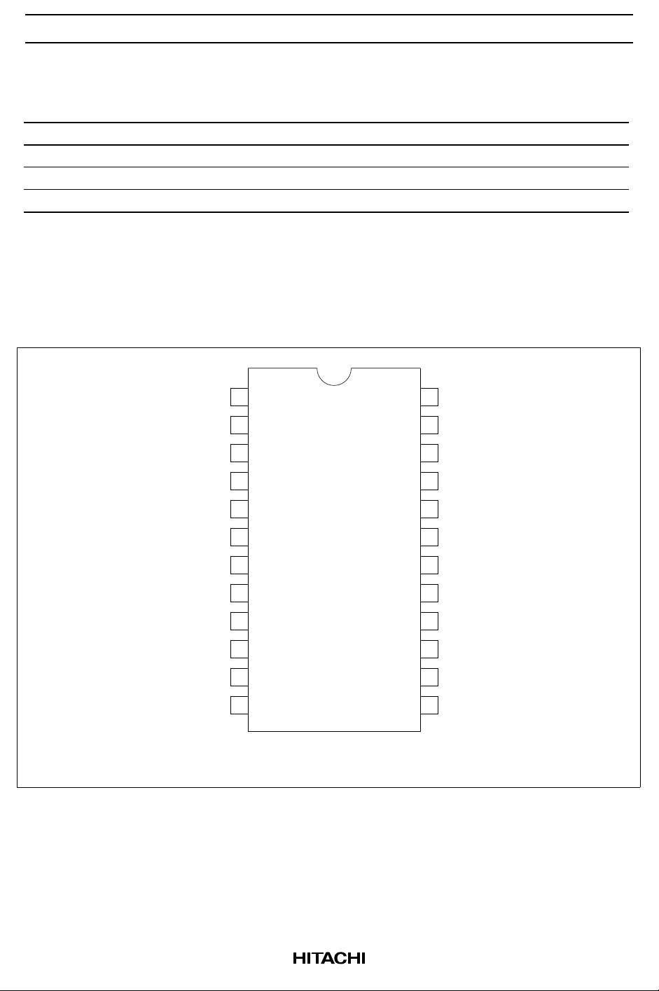
Pin Arrangement
AGND
V
CC
1Y0
1Y1
1Y2
GND
GND
1Y3
1Y4
V
CC
FBOUT
1
2
3
4
5
6
7
8
9
10
G
11
12
(Top view)
24
23
22
21
20
19
18
17
16
15
14
13
CLK
AV
CC
V
CC
1Y9
1Y8
GND
GND
1Y7
1Y6
1Y5
V
CC
FBIN
2
Page 3

HD74CDCF2510B
Absolute Maximum Ratings
Item Symbol Ratings Unit Conditions
Supply voltage V
Input voltage
Output voltage
*1
*1, 2
Input clamp current I
Output clamp current I
Continuous output current I
Supply current ICC or I
Maximum power dissipation
at Ta = 55°C (in still air)
*3
Storage temperature T
CC
V
I
V
O
IK
OK
O
GND
P
T
stg
Notes: Stresses beyond those listed under “absolute maximum ratings” may cause permanent damage
to the device. These are stress ratings only, and functional operation of the device at these or
any other conditions beyond those indicated under “recommended operating conditions” is not
implied. Exposure to absolute maximum rated conditions for extended periods may affect
device reliability.
1. The input and output negative voltage ratings may be exceeded if the input and output clamp
current ratings are observed.
2. This value is limited to 4.6 V maximum.
3. The maximum package power dissipation is calculated using a junction temperature of 150°C and
a board trace length of 750 mils.
–0.5 to 4.6 V
–0.5 to 6.5 V
–0.5 to VCC +0.5 V
–50 mA VI < 0
±50 mA VO < 0 or VO > V
±50 mA VO = 0 to V
CC
±100 mA
0.7 W
–65 to +150 °C
CC
Recommended Operating Conditions
Item Symbol Min Typ Max Unit Conditions
Supply voltage V
Input voltage V
Output current I
Operating temperature T
CC
IH
V
IL
V
I
OH
I
OL
a
Note: Unused inputs must be held high or low to prevent them from floating.
3.0 — 3.6 V
2.0 — — V
— — 0.8
0—V
CC
— — –12 mA
——12
0—85°C
3
Page 4
HD74CDCF2510B
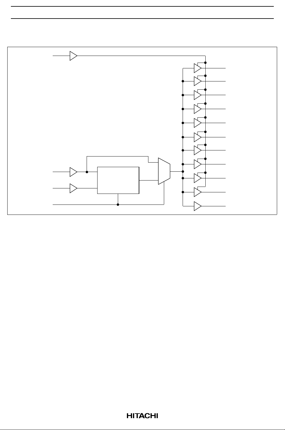
Logic Diagram
11
G
24
CLK
CC
13
23
FBIN
AV
PLL
3
4
5
8
9
15
16
17
20
21
12
1Y0
1Y1
1Y2
1Y3
1Y4
1Y5
1Y6
1Y7
1Y8
1Y9
FBOUT
4
Page 5

HD74CDCF2510B
CC
CC
Pin Function
Pin name No. Type Description
CLK 24 I Clock input. CLK provides the clock signal to be distributed by the
HD74CDCF2510B clock driver. CLK is used to provide the
reference signal to the integrated PLL that generates the clock
output signals. CLK must have a fixed frequency and fixed phase
for the PLL to obtain phase lock. Once the circuit is powered up
and a valid CLK signal is applied, a stabilization time is required for
the PLL to phase lock the feedback signal to its reference signal.
FBIN 13 I Feedback input. FBIN provides the feedback signal to the internal
PLL. FBIN must be hard-wired to FBOUT to complete the PLL. The
integrated PLL synchronizes CLK and FBIN so that there is
nominally zero phase error between CLK and FBIN.
G 11 I Output bank enable. G is the output enable for outputs 1Y(0:9).
When G is low, outputs 1Y(0:9)are disabled to a logic-low state.
When G is high, all outputs 1Y(0:9) are enabled and switch at the
same frequency as CLK.
FBOUT 12 O Feedback output. FBOUT is dedicated for external feedback. It
switches at the same frequency as CLK. When externally wired to
FBIN, FBOUT completes the feedback loop of the PLL.
1Y(0:9) 3, 4, 5, 8, 9,
15, 16, 17,
20, 21
AV
CC
23 Power Analog power supply. AVCC provides the power reference for the
AGND 1 Ground Analog ground. AGND provides the ground reference for the
V
CC
2, 10, 14, 22 Power Power supply
GND 6, 7, 18,19 Ground Ground
O Clock outputs. These outputs provide low-skew copies of CLK.
Output bank 1Y(0:9) is enabled via the G input. These outputs can
be disabled to a logic low state by deasserting the G control input.
analog circuitry. In addition, AV
for test purposes. When AV
can be used to bypass the PLL
is strapped to ground, PLL is
bypassed and CLK is buffered directly to the device outputs.
analog circuitry.
5
Page 6

HD74CDCF2510B
CC
Electrical Characteristics
Item Symbol Min Typ
Input clamp voltage V
Output voltage V
IK
OH
— — –1.2 V VCC = 3 V, II = –18 mA
VCC–0.2 — — V VCC = Min to Max, IOH = –100 µA
*1
Max Unit Test Conditions
2.1 — — VCC = 3 V, IOH = –12 mA
2.4 — — VCC = 3 V, IOH = –6 mA
V
OL
— — 0.2 VCC = Min to Max, IOL = 100 µA
— — 0.8 VCC = 3 V, IOL = 12 mA
— — 0.55 VCC = 3 V, IOL = 6 mA
Input current I
Quiescent supply
current
Input capacitance C
Output capacitance C
I
∆I
IN
CC
CC
IN
O
——±5 µAVCC = 3.6 V, VIN = VCC or GND
——10µAAVCC = GND, VCC = 3.6 V,
V
= VCC or GND, IO = 0
I
— — 500 µAAVCC = GND, VCC = 3.3 to 3.6 V
One input at V
Other inputs at V
—4—pFV
—6—pFV
= 3.3 V, VI = VCC or GND
CC
= 3.3 V, VO = VCC or GND
CC
–0.6 V,
or GND
CC
Note: 1. For conditions shown as Min or Max, use the appropriate value specified under recommended
operating conditions.
6
Page 7

HD74CDCF2510B
Switching Characteristics (CL = 25 pF, Ta = 0 to 85°C)
Item Symbol VCC = 3.3 V±0.3 V Unit From (Input) To (Output)
Min Typ Ma x
Phase error time t
Between output pins skew *1t
pe
sk (O)
–125 — 125 ps 66 MHz <
FBIN↑
CLKIN↑
≤ 133 MHz
— — 150 ps Any Y or FBOUT Any Y or
FBOUT
Cycle to cycle jitter –75 — 75 ps F (clkin =
133 MHz)
Duty cycle 45 — 55 % F (clkin =
66 to 133 MHz)
Any Y or
FBOUT
Any Y or
FBOUT
Slew rate 5.0 — 1.0 volts/ns Any Y or
FBOUT
Analog power supply
Vapsr
*2
100 — — mV
P–P
AV
CC
rejection
(DC to 10 MHz)
Notes: The specifications for parameters in this table are applicable only after any appropriate
stabilization time has elapsed.
1. The t
specification is only valid for equal loading of all outputs.
sk(O)
2. This parameter is characterized but not tested.
Timing requirements
Item Symbol Min Max Unit Test Conditions
Input clock frequency f
clock
Input clock duty cycle 40 60 %
Stabilization time
*1
Note: 1. Time required for the integrated PLL circuit to obtain phase lock of its feedback signal to its
reference signal. In order for phase lock to be obtained, a fixed-frequency, fixed-phase
reference signal must be present at CLK. Until phase lock is obtained, the specifications for
propagation delay and skew parameters given in the switching characteristics table are not
applicable.
50 140 MHz
— 1 ms After power up
7
Page 8

HD74CDCF2510B
Test Circuit
From output
under test
*1
C = 25 pF
L
Note: 1. CL includes probe and jig capacitance.
Waveforms – 1
Input
50% V
CC
50% V
500 Ω
3 V
CC
0 V
V
Output
(=FBOUT)
50% V
0.4 V
CC
2 V 2 V
t
TLH
t
THL
0.4 V
OH
V
OL
Notes: 1. All input pulses are supplied by generators having the following characteristics: PRR ≤ 100
MHz, ZO = 50 Ω, tr = 1.2 ns, tf = 1.2 ns.
2. The outputs are measured one at a time with one transition per measurement.
8
Page 9

Waveforms – 2
CLKIN
FBIN
FBOUT
Any Y
t
phase error
t
sk (o)
HD74CDCF2510B
Any Y
Any Y
t
sk (o)
9
Page 10

HD74CDCF2510B
Package Dimensions
7.80
8.10 Max
24 13
112
+0.08
0.22
–0.07
0.20 ± 0.06
0.65 Max
0.65
0.13
Unit : mm
4.4
1.0
M
6.4 ± 0.2
0.10
1.10 Max
Dimension including the plating thickness
Base material dimension
0.17 ± 0.05
0.15 ± 0.04
+0.03
–0.04
0.07
0° – 8°
Hitachi Code
JEDEC
EIAJ
Weight
(reference value)
0.5 ± 0.1
TTP-24DB
—
—
0.08 g
10
Page 11

HD74CDCF2510B
Cautions
1. Hitachi neither warrants nor grants licenses of any rights of Hitachi’s or any third party’s patent,
copyright, trademark, or other intellectual property rights for information contained in this document.
Hitachi bears no responsibility for problems that may arise with third party’s rights, including
intellectual property rights, in connection with use of the information contained in this document.
2. Products and product specifications may be subject to change without notice. Confirm that you have
received the latest product standards or specifications before final design, purchase or use.
3. Hitachi makes every attempt to ensure that its products are of high quality and reliability. However,
contact Hitachi’s sales office before using the product in an application that demands especially high
quality and reliability or where its failure or malfunction may directly threaten human life or cause risk
of bodily injury, such as aerospace, aeronautics, nuclear power, combustion control, transportation,
traffic, safety equipment or medical equipment for life support.
4. Design your application so that the product is used within the ranges guaranteed by Hitachi particularly
for maximum rating, operating supply voltage range, heat radiation characteristics, installation
conditions and other characteristics. Hitachi bears no responsibility for failure or damage when used
beyond the guaranteed ranges. Even within the guaranteed ranges, consider normally foreseeable failure
rates or failure modes in semiconductor devices and employ systemic measures such as fail-safes, so that
the equipment incorporating Hitachi product does not cause bodily injury, fire or other consequential
damage due to operation of the Hitachi product.
5. This product is not designed to be radiation resistant.
6. No one is permitted to reproduce or duplicate, in any form, the whole or part of this document without
written approval from Hitachi.
7. Contact Hitachi’s sales office for any questions regarding this document or Hitachi semiconductor
products.
Hitachi, Ltd.
Semiconductor & Integrated Circuits.
Nippon Bldg., 2-6-2, Ohte-machi, Chiyoda-ku, Tokyo 100-0004, Japan
Tel: Tokyo (03) 3270-2111 Fax: (03) 3270-5109
URL NorthAmerica : http:semiconductor.hitachi.com/
For further information write to:
Hitachi Semiconductor
(America) Inc.
179 East Tasman Drive,
San Jose,CA 95134
Tel: <1> (408) 433-1990
Fax: <1>(408) 433-0223
Europe : http://www.hitachi-eu.com/hel/ecg
Asia (Singapore) : http://www.has.hitachi.com.sg/grp3/sicd/index.htm
Asia (Taiwan) : http://www.hitachi.com.tw/E/Product/SICD_Frame.htm
Asia (HongKong) : http://www.hitachi.com.hk/eng/bo/grp3/index.htm
Japan : http://www.hitachi.co.jp/Sicd/index.htm
Hitachi Europe GmbH
Electronic components Group
Dornacher Stra§e 3
D-85622 Feldkirchen, Munich
Germany
Tel: <49> (89) 9 9180-0
Fax: <49> (89) 9 29 30 00
Hitachi Europe Ltd.
Electronic Components Group.
Whitebrook Park
Lower Cookham Road
Maidenhead
Berkshire SL6 8YA, United Kingdom
Tel: <44> (1628) 585000
Fax: <44> (1628) 778322
Hitachi Asia Pte. Ltd.
16 Collyer Quay #20-00
Hitachi Tower
Singapore 049318
Tel: 535-2100
Fax: 535-1533
Hitachi Asia Ltd.
Taipei Branch Office
3F, Hung Kuo Building. No.167,
Tun-Hwa North Road, Taipei (105)
Tel: <886> (2) 2718-3666
Fax: <886> (2) 2718-8180
Copyright ' Hitachi, Ltd., 2000. All rights reserved. Printed in Japan.
Hitachi Asia (Hong Kong) Ltd.
Group III (Electronic Components)
7/F., North Tower, World Finance Centre,
Harbour City, Canton Road, Tsim Sha Tsui,
Kowloon, Hong Kong
Tel: <852> (2) 735 9218
Fax: <852> (2) 730 0281
Telex: 40815 HITEC HX
11
 Loading...