

Page 1

HD74BC574A
Octal D Type Flip Flops With 3 State Outputs
ADE-205-042 (Z)
Rev. 0
June 1993
Description
The HD74BC574A provides high drivability and operation equal to or better than high speed bipolar
standard logic IC by using Bi-CMOS process. The device features low power dissipation that is about 1/5
of high speed bipolar logic IC, when the frequency is 10 MHz. The device has eight edge triger D type flip
flops with three state outputs in a 20 pin package. Data at the D inputs meeting set up requirements, are
transferred to the Q outputs on positive going transitions of the clock input. When the latch enable goes
low, data at the D inputs will be retained at the outputs until latch enable returns high again. When a high
logic level is applied to the output control input, all outputs go to a high impedance state, regardless of what
signals are present at the other inputs and the state of the strage elements.
Features
• Input/Output are at high impedance state when power supply is off.
• Built in input pull up circuit can make input pins be open, when not used.
• TTL level input
• Wide operating temperature range
Ta = –40 to + 85°C
Page 2
HD74BC574A
Function Table
Inputs
Output Control CK D Output Q
L HH
L LL
LLXQ
HX X Z
H : High level
L : Low level
X : Immaterial
Z : High impedance
: Low to high transition
: Level of Q before the indicated steady state input conditions were established.
Q
0
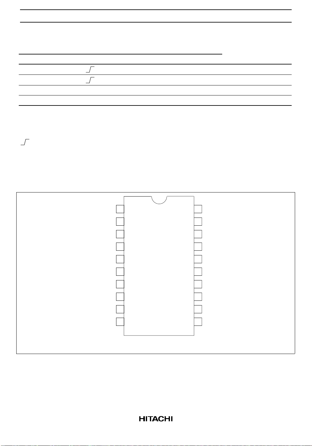
Pin Arrangement
0
Output
Control
1D
2D
3D
4D
5D
6D
7D
8D
GND
1
2
3
4
5
6
7
8
9
10
(Top view)
20
19
18
17
16
15
14
13
12
11
V
1Q
2Q
3Q
4Q
5Q
6Q
7Q
8Q
CK
CC
2
Page 3
HD74BC574A
Absolute Maximum Ratings
Item Symbol Rating Unit
Supply voltage V
Input diode current I
Input voltage V
Output voltage V
Off state output voltage V
CC
IK
IN
OUT
OUT(off)
Storage temperature Tstg –65 to +150 °C
Note: 1. The absolute maximum ratings are values which must not individually be exceeded, and
furthermore, no two of which may be realized at the same time.
Recommended Operating Conditions
Item Symbol Min Typ Max Unit
Supply voltage V
Input voltage V
Output voltage V
CC
IN
OUT
Operating temperature Topr –40 — 85 °C
Input rise/fall time*
1
tr, t
f
Note: 1. This item guarantees maximum limit when one input switches.
Waveform: Refer to test circuit of switching characteristics.
4.5 5.0 5.5 V
0—VCCV
0—VCCV
0 — 8 ns/V
–0.5 to +7.0 V
±30 mA
–0.5 to +7.5 V
–0.5 to +7.5 V
–0.5 to +5.5 V
3
Page 4

HD74BC574A
Logic Diagram
Output
Control
1D
2D
3D
4D
8D
CK
D Q
CK
D Q
CK
D Q
CK
D Q
CK
D Q
CK
1Q
2Q
3Q
4Q
8Q
4
Page 5

HD74BC574A
Electrical Characteristics (Ta = –40°C to +85°C)
Item Symbol VCC (V) Min Max Unit Test Conditions
Input voltage V
Output voltage V
IH
V
IL
OH
4.5 2.4 — V IOH = –3 mA
4.5 2.0 — V IOH = –15 mA
V
OL
4.5 — 0.4 V IOL = 24 mA
4.5 — 0.5 V IOL = 48 mA
Input diode voltage V
Input current I
IK
I
4.5 — –1.2 V IIN = –18 mA
5.5 — –250 µAV
5.5 — 1.0 µAV
5.5 — 100 µAV
Short circuit output current*1I
Off state output current I
Supply current I
OS
OZH
I
OZL
CCL
I
CCH
I
CCZ
2
I
*
CCT
5.5 –100 –225 mA VIN = 0 or 5.5 V
5.5 — 50 µAV
5.5 — –50 µAV
5.5 — 29.5 mA VIN = 0 or 5.5 V
5.5 — 2.5 mA VIN = 0 or 5.5 V
5.5 — 2.5 mA VIN = 0 or 5.5 V
5.5 — 1.5 mA VIN = 3.4 or 0.5 V
Notes: 1. Not more than one output should be shorted at a time and duration of the short circuit should not
exceed one second.
2. When input by the TTL level, it shows I
2.0 — V
— 0.8 V
increase at per one input pin.
CC
= 0 V
IN
= 5.5 V
IN
= 7.0 V
IN
= 2.7 V
O
= 0.5 V
O
All outputs is “L”
All outputs is “H”
All outputs is “Z”
5
Page 6

HD74BC574A
Switching Test Method (CL = 50 pF)
Ta = 25°C
V
= 5.0 V
CC
Ta = –40 to 85°C
VCC = 5.0 V ±10%
Item Symbol Min Max Min Max Unit Test conditions
Propagation CK → Qt
delay time t
Output enable time t
t
Output disable time t
t
PLH
PHL
ZH
ZL
HZ
LZ
3.0 8.0 3.0 10.0 ns See under figure
3.0 8.0 3.0 10.0
3.0 9.0 3.0 11.0 ns
3.0 9.0 3.0 11.0
3.0 8.0 3.0 10.0 ns
3.0 8.0 3.0 10.0
Setup time ts(H) 2.0 — 2.0 — ns
ts(L) 2.0 — 2.0 —
Hold time th(H) 2.0 — 2.0 — ns
th(L) 2.0 — 2.0 —
Pulse width tW(H) 6.0 — 6.0 — ns
tW(L) 6.0 — 6.0 —
Input capacitance C
Output capacitance C
IN
O
3.0 (Typ) — — pF VIN = VCC or GND
15.0 (Typ) — pF VO = VCC or GND
Test Circuit
V
V
CC
OC
1D to 8D
CK
Pulse Generator
Z
out
= 50
Ω
Pulse Generator
Z
out
= 50
Ω
Input
Input
See Function Table
Notes: 1. CL includes probe and jig capacitance.
2. OPEN: t
7 V: tZL, t
PLH
LZ
, t
PHL
, tZH, tHZ,th, ts t
CC
1Q to 8Q
w
Output
C =
L
50 pF
50 ScopeΩ
500 Ω
450 Ω
*2
OPEN
7V
6
Page 7

Waveforms-1
HD74BC574A
Input
CK
Input
D
Output
Q
Waveforms-2
t
r
90%
90%
1.5 V
10%
t
r
90%
1.5 V
t
10%
90%
f
t
10% 10%
t
PLH
1.5 V
t
r
3 V
1.5 V
0 V
f
3 V
0 V
t
PHL
V
OH
1.5 V
V
OL
t
f
Input
CK
Input
D
90% 90%
1.5 V
10%
t
sh
1.5 V
1.5 V
10%
t
w
t
1.5 V
3 V
0 V
3 V
0 V
7
Page 8

HD74BC574A
Waveforms-3
Output
Control
1.5 V
10%
Waveform–A
Waveform–B
Notes: 1. tr = 2.5 ns, tf = 2.5 ns
2. Input waveform: PRR = 1 MHz, duty cycle 50%
3. Waveform-A shows input conditions such that the output is “L” level when enable by the output
control.
4. Waveform-B shows input conditions such that the output is “H” level when enable by the output
control.
t
f
t
r
90%90%
3 V
1.5 V
10%
t
ZL
t
LZ
0 V
3.5 V
1.5 V
V
+ 0.3 V
OL
t
ZH
t
HZ
V
– 0.3 V
OH
V
OL
V
OH
1.5 V
0 V
8
Page 9

Package Dimensions
HD74BC574A
Unit: mm
9
Page 10

Cautions
1. Hitachi neither warrants nor grants licenses of any rights of Hitachi’s or any third party’s patent,
copyright, trademark, or other intellectual property rights for information contained in this document.
Hitachi bears no responsibility for problems that may arise with third party’s rights, including
intellectual property rights, in connection with use of the information contained in this document.
2. Products and product specifications may be subject to change without notice. Confirm that you have
received the latest product standards or specifications before final design, purchase or use.
3. Hitachi makes every attempt to ensure that its products are of high quality and reliability. However,
contact Hitachi’s sales office before using the product in an application that demands especially high
quality and reliability or where its failure or malfunction may directly threaten human life or cause risk
of bodily injury, such as aerospace, aeronautics, nuclear power, combustion control, transportation,
traffic, safety equipment or medical equipment for life support.
4. Design your application so that the product is used within the ranges guaranteed by Hitachi particularly
for maximum rating, operating supply voltage range, heat radiation characteristics, installation
conditions and other characteristics. Hitachi bears no responsibility for failure or damage when used
beyond the guaranteed ranges. Even within the guaranteed ranges, consider normally foreseeable
failure rates or failure modes in semiconductor devices and employ systemic measures such as failsafes, so that the equipment incorporating Hitachi product does not cause bodily injury, fire or other
consequential damage due to operation of the Hitachi product.
5. This product is not designed to be radiation resistant.
6. No one is permitted to reproduce or duplicate, in any form, the whole or part of this document without
written approval from Hitachi.
7. Contact Hitachi’s sales office for any questions regarding this document or Hitachi semiconductor
products.
Hitachi, Ltd.
Semiconductor & Integrated Circuits.
Nippon Bldg., 2-6-2, Ohte-machi, Chiyoda-ku, Tokyo 100-0004, Japan
Tel: Tokyo (03) 3270-2111 Fax: (03) 3270-5109
URL NorthAmerica : http:semiconductor.hitachi.com/
For further information write to:
Hitachi Semiconductor
(America) Inc.
179 East Tasman Drive,
San Jose,CA 95134
Tel: <1> (408) 433-1990
Fax: <1>(408) 433-0223
Europe : http://www.hitachi-eu.com/hel/ecg
Asia (Singapore) : http://www.has.hitachi.com.sg/grp3/sicd/index.htm
Asia (Taiwan) : http://www.hitachi.com.tw/E/Product/SICD_Frame.htm
Asia (HongKong) : http://www.hitachi.com.hk/eng/bo/grp3/index.htm
Japan : http://www.hitachi.co.jp/Sicd/indx.htm
Hitachi Europe GmbH
Electronic components Group
Dornacher Stra§e 3
D-85622 Feldkirchen, Munich
Germany
Tel: <49> (89) 9 9180-0
Fax: <49> (89) 9 29 30 00
Hitachi Europe Ltd.
Electronic Components Group.
Whitebrook Park
Lower Cookham Road
Maidenhead
Berkshire SL6 8YA, United Kingdom
Tel: <44> (1628) 585000
Fax: <44> (1628) 778322
Hitachi Asia Pte. Ltd.
16 Collyer Quay #20-00
Hitachi Tower
Singapore 049318
Tel: 535-2100
Fax: 535-1533
Hitachi Asia Ltd.
Taipei Branch Office
3F, Hung Kuo Building. No.167,
Tun-Hwa North Road, Taipei (105)
Tel: <886> (2) 2718-3666
Fax: <886> (2) 2718-8180
Copyright ' Hitachi, Ltd., 1999. All rights reserved. Printed in Japan.
Hitachi Asia (Hong Kong) Ltd.
Group III (Electronic Components)
7/F., North Tower, World Finance Centre,
Harbour City, Canton Road, Tsim Sha Tsui,
Kowloon, Hong Kong
Tel: <852> (2) 735 9218
Fax: <852> (2) 730 0281
Telex: 40815 HITEC HX
 Loading...