

Page 1

HA13571FR
Combo (Spindle & VCM) Driver for HDD
ADE-207-269 (Z)
1st Edition
February 1999
Description
The HA13571FR is combination of Spindle and VCM Driver designed for HDD and have following
functions and features.
Functions
• 2.2 A/phase spindle motor driver
• 1.5 A VCM driver
• Soft switching control circuit
• B-EMF detection circuit
• Selectable PWM or linear drive (spindle motor driver)
• Power down brake & retract
• PWM DAC & filter (VCM driver)
• 5 V, 12 V power supply monitor
• Watch dog timer
Features
• Low thermal resistance package (θj-a ≤ 25°C/W)
• Full programable commutation structure
• Low output saturation voltage
Spindle motor driver
VCM driver
• Built-in PWM DAC with filter
• Low noise drive by soft switching
Page 2
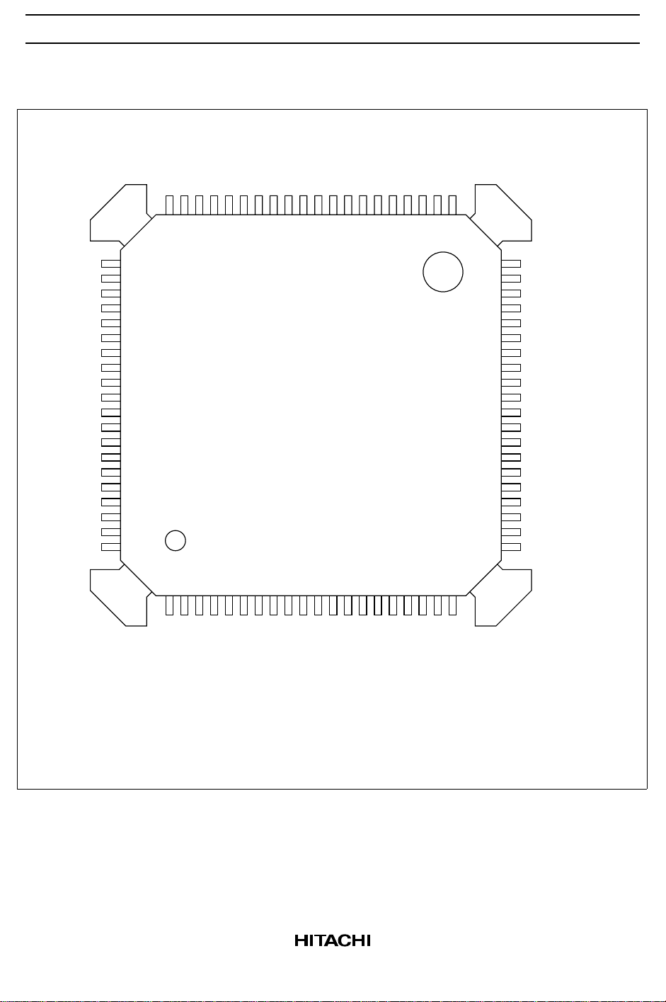
HA13571FR
Pin Arrangement
RETADJ
NC1
VCMN
NC
NC
BSTFLT
BSTCP1
BSTCP2
OSCTC
GND
GND
SDRVW
NC
SISENH
SISINK
SISINK
NC
SDRVN
SCOMP
SDRVU
61
62
63
64
65
66
67
68
69
70
71
72
73
74
75
76
77
78
79
80
VISENHNCVCMP
60
1 2 3 4 5 6 7 8 9 1011121314151617181920
VCMP
VCMP
VCCV12
SHPWR
POR12VADJ
VCMREF
WDTIN
GNDNCGND
595857 56 555453 52 515049 48 474645 44 434241
VISENL
POR5VADJ
CPORNCPORN
VISENS
VCMINP
40
39
38
37
36
35
34
33
32
31
30
29
28
27
26
25
24
23
22
21
VFLTOUT
VFLTINP
VFLTINP
VREFOUT
VPCNTL
VIPWMH
VIPWML
NC
NC
NC
NC
GND
NC
VCCA12
SENU
SENV
SENWIS
SCNTL1
SCNTL2
GND (CTLAMP)
2
Notes: 1.
NC
NC
NC
NC
TEMP
SDRVV
SLOPEC
SPWMTC
All same name pins must be connected together.
2.
"NC" and "NC1" denotes no connection pins.
3.
ALL "NC" pins must be connected to GND or opened.
4.
"NC1" pin must be connected to VCMN or opened.
VCCS12
(Top view)
NC
GND
SISENL
NC
GND
SLOPER
VCC5
SIPWM
SPWMFLT
SMODE
SCNTL3
Page 3
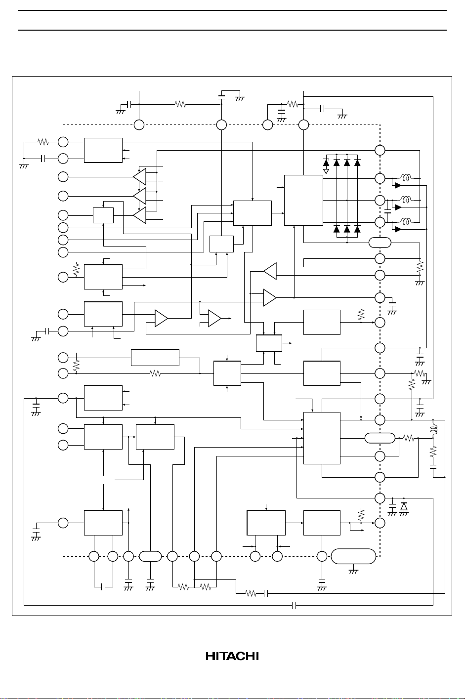
Block Diagram
HA13571FR
SLOPER
SLOPEC
SENU
SPWMFLT
VREFOUT
VIPWML
VIPWMH
OSCTC
15
3
26
25SENV
24SENWIS
23SCNTL1
22SCNTL2
20SCNTL3
0.5VCC5
19SMODE
18SIPWM
17
0.5VCC5
51WDTIN
36VPCNTL
37
34
35
69
SOFT
SWITCH
CONTROL
MPX
SMODE
COMP
PWM
DECODER
FILTER
SLEEP
VREFOUT
4.0V
PWM
DECODER
SLEEP
BOOSTER
BST
BST
CP2
CP2
0.1µF
SLEEP
SOFT
0.75VCC5
0.25VCC5
0.5VCC5
WATCH DOG
SLEEP
VREF 1.4V
VBST
BST
FLT
5V
16
−
+
−
+
−
+
INDUCTANCE
MODE
PWM MODE
LINEAR
−
+
TIMER
FILTER
VFLT
INP
34kΩ
SLEEP
U
V
W
ICOMP
4038,39
VFLT
OUT
SPWMTCVCC5
Icomp
4166
470pF
5
ONE
SHOT
SOFT
−
+
0.9V
0.75VCC5
VTRI-
LEVEL
0.25VCC5
VISENS POR
VCM
INP
VCCA12
VBST
LOGIC
DECODER
DISABLE
ISENSE
AMP
ISENSE
SLEEP
DISABLE
VCCV12/2
VREF 1.4V
POWER
MONITOR
POR
5V
ADJ
Rx
SPN
DRIVER
+
−
−
+
CONTROL
AMP
TSD
SLEEP
POR
VBST
VCM ENABLE
5/32 VCCV125/16 VCC5
12V
ADJ
12V
0.47µF
VCCS12
827
TAB
U
V
W
THERMAL
SHUT
DOWN
RETRACT
DRIVER
VCM
DRIVER
POR
DETECTOR
4553466867 42
CPOR
5V
56,57,58
5V
POR
11,14,21,29,
48,50,70,71
SDRVN
78
SDRVU
80
SDRVV
1
72
75,76
SISENH
74
10
SISENL
SCOMP
79
2
TEMP
SHPWR
54
RETADJ
61
VCCV12
55
VCMN
63
VCMP
47
VISENL
VISENH
60
VCMREF
52
43 PORN
SDRVW
SISINK
Rnf
Rs
Rf
Cf
SBD1
C133
3
Page 4

HA13571FR
Truth Table
Table 1 Input to Output Drivers
SCNTL1 SCNTL2 SCNTL3 SDRVU SDRVV SDRVW
HHLLZH
HLLZLH
HLHHL Z
LLHHZL
LHHZHL
LHLLHZ
LLLZZZ
HHHLL L
Note: Z = High impedance
Table 2 Spindle Driver Mode Control
SMODE SIPWM Spindle Driver Mode
H Duty ≥ 50% Linear Mode (High slew rate) *
H Duty ≤ 40% Linear Mode (Low slew rate) *
M X Inductive Sense Mode
L X B-EMF Sense in PWM Drive Mode
Note: 1. X = Don’t care
2. Slew rate mode is commutated at synchronized with the up edge of SLOPEC.
2
2
Table 3 VCM Control
WDTIN VPCNTL VCM Mode
H or L X Park
M H Enable
M M Disable
M L Park
Table 4 Temp Output
TEMP Status
H Warning or TSD
L Normal
4
Page 5

Table 5 Output Status
HA13571FR
PORN TSD SLEEP *
Driver L H Inactive Active L H L H
SPN Output Brake for
Retract
VCM Output Retract
(Power off)
Notes: 1. X = Don’t care
2. Z = High impedance
3. SLEEP SCNTL1 = SCNTL2 = SCNTL3 = Low
WDTIN = VPCNTL = Middle
Enable X Z X Z X
Enable X Z X Z X
3
TEMP
5
Page 6
HA13571FR
Table 6 SCNTL, WDTIN and VPCNTL Mode
SCNTL WDTIN VPCNTL Modes of Operation
Input States Input State Input State at Power Good (PORN = H)
SCNTL1 SCNTL2 SCNTL3 Spindle Driver
See Table 1 See Table 1 See Table 1 X X Enable
L L L X X Disable
H H H X X Brake
SCNTL WDTIN VPCNTL Modes of Operation
Input States Input State Input State at Power Good (PORN = H)
SCNTL1 SCNTL2 SCNTL3 VCM Driver
X X X L or H X Park
X X X Middle H Enable
X X X Middle Z Disable
X X X Middle L Park
SCNTL WDTIN VPCNTL Modes of Operation
Input States Input State Input State at Power Good (PORN = H)
SCNTL1 SCNTL2 SCNTL3 Spindle & VCM Driver
L L L Middle Z Sleep Mode *
Note: Sleep signal is generated by SCNTL and VPCNTL.
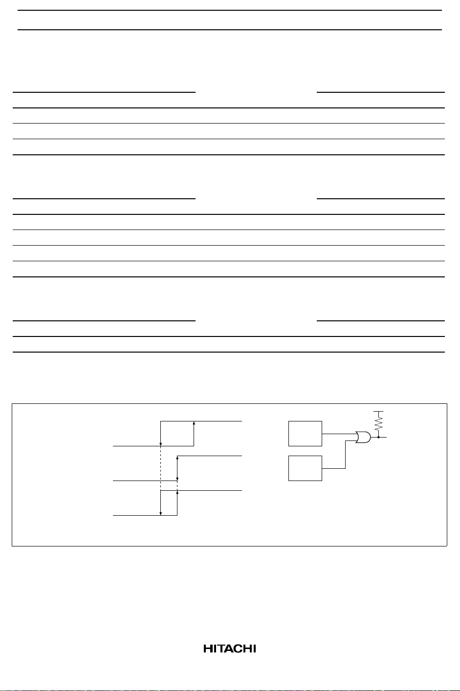
TEMP output is depend on internal TSD and internal TEMP. (see figure 1)
TEMP (Internal)
TEMP (Output)
6
Tsoff
ThysTSD (Internal)
Twar
TEMP output logic (1) TEMP output logic (2)
TSD
TEMP
Figure 1 TEMP Output Logic
TEMP
Page 7

Table 7 Function Powered on Vs Mode Operation
HA13571FR
Function
UPPER
BOOSTER
UPPER
DRIVERS
LOWER
DRIVERS COMP
CONTROL
AMP
Spindle enable ON ON ON ON ON
Spindle disable ON OFF OFF ON OFF
PORN low OFF OFF ON OFF OFF
1
Park *
2
Sleep *
Function
ON ON/OFF ON/OFF ON ON/OFF
OFF OFF OFF OFF OFF
ONE
SHOT
ICOMP
(Current
comparator)
PWM
DECODER
FILTER
SMODE
COMP
ISENSE
AMP
LOGIC
DECODER
Spindle enable ON ON ON ON ON ON
Spindle disable ON ON ON ON ON ON
PORN low OFF OFF OFF OFF OFF ON
1
Park *
2
Sleep *
Function
ON ON ON ON ON ON
OFF OFF OFF OFF OFF ON
PWM
DECODER
12V and
5V COMP
FILTER
AMP
PORN
DETECTOR
RETRACT
CIRCUIT TSD
VCM enable ON ON ON ON OFF ON
VCM disable ON ON ON ON OFF ON
1
Park *
Sleep *
2
ON ON ON ON ON ON
OFF ON OFF ON OFF ON
PORN low OFF ON OFF ON ON ON
Function VPCNTL
VREFOUT
BUF VREFOUT SENSE1
VCM
DRIVER
SLEEP
FUNCTION
VCM enable ON ON ON ON ON OFF
VCM disable ON ON ON ON OFF OFF
1
Park *
Sleep *
2
ON ON ON ON OFF OFF
ON OFF OFF OFF OFF ON
PORN low ON OFF OFF OFF OFF ON
Note: 1. Park signal is generated by VPCNTL.
2. Sleep signal is generated by SCNTL and VPCNTL.
7
Page 8

HA13571FR
Timing Chart
1. SPN Input to Output Drivers
• Control Lines
SCNTL1
SCNTL2
SCNTL3
• Output Drivers
PWM Mode
SDRVU
PWM PWM
Z
Z
ZZZ
SDRVV
SDRVW
• Output Drivers
Linear Mode
SDRVU
SDRVV
SDRVW
• Comparators
SENU
SENV
SENW
PWM
Z
PWM PWM PWM
Z Z Z
Z
Z Z Z
Z Z
Z
Z Z
PWM
Z
Z
Z Z
Z
Z Z
PWM
Z
Z
ZZZ
Note: "Z" = High impedance
8
Page 9

2. Soft Switching
B-EMF 0
• Control Lines
SCNTL1
SCNTL2
SCNTL3
• Output Voltage
SDRVU
SDRVV
HA13571FR
UVW
0
0
SDRVW
• Output Current
SDRVU
SDRVV
SDRVW
• Comparators
SENU
SENV
SENW
0
0
0
0
9
Page 10

HA13571FR
Application
ASIC
µPC
ADC
R108
C117
0.47µ
C101
4.7µ
C102
470p
0.047µ
1000p
R102
R103
R106
C113
C103
C119
C104
R101
34k
VCC5 VCCS12VCCA12
SPWMTC
SLOPER
SLOPEC
SENU
SENV
SENWIS
SCNTL1
SCNTL2
SCNTL3
SMODE
SIPWM
VIPWML
VIPWMH
SPWMFLT
WDTIN
TEMP
PORN
VPCNTL
VFLTINP
VREFOUT
VFLTOUT
VCMINP
VISENS
R107 C116
5V
Ry
15
C114
1.0µ
SDRVN
SDRVU
SDRVV
SDRVW
SISINK
SISENH
SISENL
SCOMP
GND (CTLAMP)
OSCTC
BSTCP1
BSTCP2
BSTFLT
HA13571FR
SHPWR
VCCV12
RETADJ
VISENL
VISENH
VCMREF
POR12VADJ
POR5VADJ
TAB
C133
4.7µ
VCMN
VCMP
CPOR
C105
0.22µ
Rx 15
C118
0.02µ
R2
C112
0.47µ
Rnf
0.33
C109
0.1µ
C108
2.2µ
C107
2.2µ
R1
C111
0.47µ
C110
390p
Rs
0.33
C120
0.01µ
C131
220p
C132
220p
SBD1
Unit R : Ω
D1
D2
D3
C115
0.47µ
12V
C121
4.4µ
Rf
Cf
C : F
10
Page 11

HA13571FR
External Components
Reccomended
Parts No.
R1, R2 — Setting of Retract voltage
R101 34 kΩ PWM time off for Spindle driver
R102, R103 — Setting of VCM driver gain
R106 100 kΩ Time constant for Soft switching
R107 — Phase compensation for VCM driver
R108 TBD for Watch dog timer
Rnf 0.33 Ω Current sensing for Spindle driver
Rs 0.33 Ω Current sensing for VCM driver
Rx, Ry 15 Ω for Filter VCCA12 and VCC5
Rf — Snubber for VCM driver
C101 4.7 µF 5V power supply by passing
C102 470 pF PWM time off for Spindle driver
C103 0.047 µF PWM filter for Spindle driver
C104 1000 pF PWM filter for VCM driver
C105 0.22 µF Delay for POR
C107 2.2 µF Capacitor for Retract voltage supply
C108 2.2 µF for Booster
C109 0.1 µF for Booster
C110 390 pF Time constant for Oscillation
C111 0.47 µF Phase compensation for Spindle driver
C112 0.47 µF 12V power supply by passing
C113 0.003 µF Time constant for Soft switching
C114 1.0 µF 12V power supply by passing
C115 0.47 µF 12V power supply by passing
C116 — Phase compensation for VCM driver
C117 0.47 µF Reference output by passing
C118 0.02 µF Prevent from oscillation during PWM drive
C119 TBD for Watch dog timer
C120 0.01 µF Reduction of noise from 12V power supply for VCM driver
C121 4.4 µF Reduction of noise from 12V power supply for VCM driver
C131 220 pF (Option) Filter for POR12VADJ
C132 220 pF (Option) Filter for POR5VADJ
C133 * 4.7 µF Reduction of noise from 12V power supply for VCM driver
Value Purpose
11
Page 12

HA13571FR
External Components (cont)
Reccomended
Parts No.
Cf — Snubber for VCM Driver
D1 to D3 TBD Power rectification for Retract driver
SBD1 * HRU0302A Prevent of malfunction for Retract driver
Note: Retract circuit sometime will be malfunctioning by means of negative voltage on the terminal
VCMREF (pin 52) in the following sequence.
If you want to countermeasure this, you need to avoid the following sequence or to attach the
Schottky Barrier Diode (SBD1) between terminal VCMREF and GND. (see figure 2)
1. Spindle motor driver is active and VCM driver is disable by (VPCNTL = Middle).
2. Power supply goes to low level after above condition 1 and retract circuit becomes active by
(POR = L).
Value Purpose
C117
0.47µF
37 VREFOUT
C133
4.7µF
Figure 2
52VCMREF
C120
0.01µF
SBD1
HRU0302A
12
Page 13

HA13571FR
Absolute Maximum Ratings (Ta = 25°C)
Item Symbol Rating Unit Notes
Supply voltage +12V Vcc12 –0.3 to 13.5 V 1
Supply voltage +5V Vcc5 –0.3 to 6 V 1
Output voltage +12V (DC) Vsdrv (DC) –0.3 to 15 V 5
Output voltage +12V (PEAK) Vsdrv (PEAK) –2.0 to 17 V 5, 6
Output voltage +5V Vout –0.3 to 6 V 7
Output current spindle driver Iospn (DC) 2.2 A 2
Output current VCM driver Iovcm (DC) 1.5 A 2
Input voltage Vi –0.3 to Vcc5 V 3
Power dissipation P
Junction temperature Tj 160 °C1
Storage temperature Tstg –55 to +125 °C
Notes: 1. Operating range are as follows.
Vcc12 = 10.8 to 13.2 V
VccA12 = 10.4 to 13.2 V
Vcc5 = 4.3 to 5.5 V
Tjopr = 0 to 130°C
2. Refer to ASO shown below. Operating locus must be within the ASO.
3. Applied to pin SCNTL1, SCNTL2, SCNTL3, SMODE, SIPWM, VPCNTL, VIPWML and VIPWMH.
4. Thermal resistance θj-a ≤ 25°C/W with 4 layer multi glass-epoxy board.
5. Applied to pin SDRVN, SDRVU, SDRVV, SDRVW, VCMN and VCMP.
6. PEAK time must be shorter than 1 ms.
7. Applied to pin PORN and TEMP.
T
5W4
2.2
2.0
1.0
0.5
0.2
Corrector Current Ic (A)
0.1
The voltage between Corrector and Emitter Vce (V) The voltage between Corrector and Emitter Vce (V)
Spindle Driver VCM Driver
2.0
t = 1ms
t = 10ms
t = 100ms
210152015
1.0
0.5
0.2
Corrector Current Ic (A)
0.1
t = 1ms
t = 10ms
t = 100ms
210152015
Figure 3 ASO
13
Page 14

HA13571FR
Electrical Characteristics (Ta = 25°C, Vcc5 = 5.0 V, Vcc12 = 12 V)
Applica-
Item Symbol Min Typ Max Unit Test Conditions
+5V supply current Icc5s — 9.0 11.5 mA Sleep mode VCC5
Icc5 — 15 18.5 mA
+12V supply current Icc12s — 3.0 4.5 mA Sleep mode VCCS12
Icc12 — 40 50 mA SMODE = High
IccA12 — 12.5 16 mA SMODE = High VCCA12 1
Total power dissipation Pdiss — 81 110 mW Sleep mode
Vcc5 = 5.0V,
Vcc12 = 12.0V
Logic
inputs1
Logic
inputs2
Logic
inputs3
Logic
inputs4
Input current Iin — — ±10 µA Vin = 0 to Vcc5 SCNTL1
High level voltage Vih 3.5 — — V
Low level voltage Vil — — 1.5 V
High level voltage Vih 3.9 — — V SMODE
Middle level voltage Vim 1.4 — 3.6 V
Low level voltage Vil — — 1.1 V
High level current Iih 80 100 133 µA VIN = 5V
Low level current Iil –80 –100 –133 µA VIN = 0V
High level voltage Vih 3.9 — — V VPCNTL
Middle level voltage Vim 1.4 — 3.6 V
Low level voltage Vil — — 1.1 V
High level current Iih 80 100 133 µA VIN = 5V WDTIN =
Middle
Low level current Iil –80 –100 –133 µA VIN = 0V
High level current Iih 480 600 800 µA VIN = 5V WDTIN =
High or Low
Low level current Iil –80 –100 –133 µA VIN = 0V
High level voltage Vih 3.8 — — V WDTIN
Middle level voltage Vim 1.3 — 3.5 V
Low level voltage Vil — — 1.0 V
Input current Iin — — ±20 µA Vin = 0 to Vcc5
ble pins Note
VCCV12
VCCA12
VCC5
VCCS12
VCCV12
VCCA12
SCNTL2
SCNTL3
14
Page 15

Electrical Characteristics (cont)
Item Symbol Min Typ Max Unit Test Conditions
SPN
output
drivers
SPN
PWM
DAC &
filter
PWM
one
shot
Total output
saturation voltage
Leakage current Icex1 — — 0.1 mA VIN = 14V SDRVU
Recirculating
diode forward
voltage
Overvoltage
protection clamp
Input current Iin — — ±300 µA Vin = –0.3 to Vcc5 SIPWM
High level voltage Vh 3.5 — — V
Low level voltage Vts — — 1.5 V
PWM pulse width Tpwm 23 — — ns
Output resistance
at Spwmflt
Output voltage Vflt100 — 1.79 ±10% V Duty = 100%
Sink current Isk 410 580 750 µA Spwmtg = 3.0V SPWMTC
Low clamp voltage Vclmp 1.33 1.53 1.73 V for discharging
Threshold voltage Vthst 3.0 3.3 3.6 V for discharging
Vsatspn — 1.1 1.4 V Iout = 1.2A, Tj = 25°C SDRVU
— 2.0 2.6 V Iout = 2.2A Tj = 25°C
— 2.6 3.74 V Tj = 125°C1
Icex2 — 0.6 1.2 mA Test source current
from middle phase
RL = 11Ω/phase
Ifrdu — — 20 mA Vfrdu = 2.0V,
Vcc12 = 0V
Vfrdl1 — 1.25 1.4 V If = –1.0A 1
Vfrdl2 — 1.75 2.2 V If = –2.2A
Vclp 14.4 15.4 17 V Iclp = 100mA
Rsout — 34 ±20% kΩ SPWMFLT
Vflt50 — 0.93 ±10% V Duty = 50%
Vflt0 — 50 100 mV Duty = 0%
Vthend 1.47 1.67 1.87 V for charging
HA13571FR
Applicable pins Note
SDRVV
SDRVW
SDRVV
SDRVW
15
Page 16

HA13571FR
Electrical Characteristics (cont)
Item Symbol Min Typ Max Unit Test Conditions
PWM
one
shot
B-EMF
comparators
Control
amp &
sense
amp
One-shot off time Toff 9 11 13 µs Ext. R = 34kΩ,
C = 470pF
One-shot minimum
on time
Common mode
input voltage
Common mode
clamp resistor
Offset voltage Vcos — — ±5 mV Sdrvn = 1.0V to Vcc12-2V
Output low voltage Vsink — — 0.5 V Isink = 1.0mA SENU
Output high voltage Vsource 2.7 — — V Isource = 0.04mA
Center tap voltage VCT 1.0 — VCC12
Isense input current Isen –10 — 24 µA SISENH = 0 to 0.4V SISENH
Isense amp voltage
gain
SISENH voltage V100 — 348 ±18 mV Rnf = 0.33Ω D = 100%
Current loop
bandwidth
ICOMP threshold
voltage
Ton 2.1 2.8 3.5 µs
Vcm –0.4 — VCC12
–2.0
Rclp 7 10 13 kΩ Sdrvn = 6V
∆Vosc — — ±7 mV Variation in U, V, W
–2.0
Ksp — 4.9 ±4.6% V/V Ksp = Spwmflt/Sisenh
— 348 ±18 mV D = 100%
V50 — 170 ±18 mV D = 50%
V5 — 7 17 mV D = 5%
V0 0.0 0.0 5 mV D = 0%
Bwd 1.8 3.0 — kHz Rnf = 0.33W, Rm = 12Ω
Vth — 180 ±15 mV No Load
—80±11 mV Smode = 2.5V,
V SDRVU
V SCNTL1, 2, 3 = “L”
RL = 2Ω/phase
VPCNTL = “H” or “M”
Rs = 0.33Ω
Lm = 1.0mH, C111 = 0.47µF
No Rnf
Sisenh = 0 to 5V
Tj = 125°C
Spwmflt =
1.0V
Spwmflt =
0.5V
Applicable pins Note
SPWMTC 1
SDRVV
SDRVW
SDRVN
SENV
SENWIS
SDRVN
SISENL
SISENH
SPWMFLT
SISINK 1
1
SENWIS
16
Page 17

Electrical Characteristics (cont)
Item Symbol Min Typ Max Unit Test Conditions
Soft
Switch
VCM
PWM
DAC
Filter Output
SLOPER
Output voltage
SLOPEC
Source current
SLOPEC
Sink current
SLOPEC
High voltage
SLOPEC
Low voltage
Input current Iin — — ±200 µA Vin = 0V to 5V VIPWML
Input high voltage Vhi 3.5 — — V
Input low voltage Vli — — 1.5 V
Input PWM
frequency
PWM pulse width Tpwm 23 — — ns
PWM DAC
resolution
Positive full scale
voltage
Negative full scale
voltage
Current ratio –0.5 32 +1.0 A/A MSB/LSB
Output
impedance
impedance
Phase shift — — 1.2 deg. f = 500Hz,
Cutoff frequency Fc 33 50 75 kHz ∆Gv = –3dB 1
Attenuation — 24 ±10 dB f = 200kHz
Vsoftr 1.45 1.90 2.35 V R106 = 100kΩ SLOPER
Isource 7 9 12 µA R106 = 100kΩ SLOPEC
Isink 7 9 12 µA R106 = 100kΩ
Vhsoft 3.5 4.4 5.5 V High SR
2.0 2.4 2.8 V Low SR
Vlsoft 0.9 1.1 1.3 V
Fpwm — 625 — kHz 1
— 14 — bits 1
Vflp — Vrefout
+1.0
Vfln — Vrefout
–1.0
Rout — 3.75 ±17% kΩ
Rout — — 40 Ω∆Vout = 10mV VFLTOUT
— V VFLTINP 1
—V 1
Vfltinp to Vfltout
HA13571FR
Applicable pins Note
VIPWMH
1
17
Page 18

HA13571FR
Electrical Characteristics (cont)
Item Symbol Min Typ Max Unit Test Conditions
Filter Output voltage Vflt0 — Vrefout
–2.03
Vflt50 — Vrefout ±0.05 V Vipwml & Vipwmh
Vflt100 — Vrefout
+2.03
Current
sense
amp
VCM
output
driver
Output voltage
symmetry
Input current Iin –200 — 400 µA VISENS
Output offset
voltage
Output resistance Rout — — 25 Ω Sink and Source
Visenl, Visenh
operating range
Unity gain
bandwidth
Gain G10 3.8 4.0 4.2 V/V VISENH/L = 0V
Power supply
rejection ratio
Total output
saturation voltage
Output leakage Ilk — — 0.5 mA Tj = 25°C
Output quiescent
voltage
Recircurate diode
voltage
Vfltsym — — ±140 mV | Vflt100 – Vrefout |
Vos — 10 ±20 mV Visenh – Visenl = 0V
Vr1 0 — 12 V Gain and Offset
BW1 2.0 3.0 4.0 MHz 1
G16 3.8 4.0 4.2 V/V VISENH/L = 6V
G112 3.8 4.0 4.2 V/V VISENH/L = 12V
∆G1 — 0 ±2% V/V (G112 – G16)/G16
PSRR 40 52 — dB F ≤ 20kHz 1
Vsatvcm — 1.5 1.875 V Iout = 1.5A Tj = 25°C VCMN
— 1.95 2.85 V Tj = 125°C1
Vq — Vcc12/2 ±5% V
VRD — 2.0 2.5 V Io = –1.5A 1
±0.1 V Vipwml & Vipwmh
Duty = 0%
Duty = 50%
±0.1 V Vipwml & Vipwmh
Duty = 100%
– | Vfit0 – Vrefout |
at 1/2 Vcc
Valid
(G10 – G16)/G16
BSTFLT = VCCV12 = 14V
Applicable pins Note
VFLTOUT
VISENH
VISENL
VCMP
18
Page 19

HA13571FR
Electrical Characteristics (cont)
Applica-
Item Symbol Min Typ Max Unit Test Conditions
VCM
output
driver
Retract
(Power
on)
Retract
(Power
off)
Brake Brake voltage Vbrks — 0.5 0.8 V Ibrk = 1.2A
Vrefout Output voltage Vref — 4.0 ±0.2 V Io = 10.0mA, Cl = 10nF VREFOUT
Booster Output voltage Vbst Vcc12
Output offset
current
Transconductance Gm — 0.5 ±5% A/V Vin = FLTOUT
–3dB bandwidth BW — 300 ±30% kHz Vout = VCMN, Rl = 15Ω
Total harmonic
distortion
Time of crossover
distortion
Symmetry Vcm
drivers VCMN
VCMP
Linearity Vcm
drivers VCMN
VCMP
Overvoltage
protection clamp
Reference volatge Vvcmref — Vcc12/2 ±5% V 20kΩ/20kΩ VCMREF
Output voltage Vretout 0.65 0.9 1.3 V Rs = 0.33Ω, RL = 15Ω
Saturation voltage
(Lower)
Min. retract current Iret 15 — — mA VIN = VSHPWR + VF(IM10)
Max. retract voltage
(VCMN–VCMP)
Ios — — ±28 mA Rs = 0.33Ω, Rl = 10Ω,
R102 = 10kΩ, R103 = 6.6kΩ
C106, R107 = OPEN
THD — 1.0 2.5 % f = 1kHz, Vout = 1Vrms
Tcro — 2 5 µs Ramp input
VCMINP 20µs
R102 = 10kΩ, R103 = 6.6kΩ
C106, R107 = OPEN
RATIO
= I2/I1
L =
| I2–I0 |/
| I1–I0 |
Vclp2 14.6 15.8 17.0 V Iclp2 = 100mA
VsatL — 0.12 0.25 V VCMP
Vret — — 1.3 V VIN = 8V, Rm 4Ω,
0.95 1.02 1.09 Ratio I2 = Irvcm at D = 10%
I1 = Irvcm at D = 90%
I0 = Irvcm at D = 50%
Rs = 0.33Ω, RL = 10Ω
R103/R102 = 10k/6.6k
0.99 1.02 1.05 Ratio
R1 = 33kΩ, R2 = 10kΩ
VPCNTL = “L”
VIN = 2.0–VFSub(@20mA)
R1 = 33kΩ, R2 = 10kΩ
SCNTL1 to 3 = High
+0.8
Vcc12
+0.8
Vcc12
+0.8
— Vcc12
— Vcc12
— Vcc12
V Ispn = 0A, Ivcm = 0A BSTFLT
+3.7
V Ispn = 2.2A, Ivcm = 0A
+3.7
V Ispn = 0.5A, Ivcm = 1.5A
+3.7
ble pins Note
VISENH
VCMN
VCMP
VCMN
VCMN
VCMP
SDRVU
SDRVV
SDRVW
1
19
Page 20

HA13571FR
Electrical Characteristics (cont)
Applica-
Item Symbol Min Typ Max Unit Test Conditions
Power
Monitor
POR
detector
Thermal
shutdown
OSC Frequency range fosc 200 250 300 kHz OSCTC
TEMP Output low voltage Vol2 — — 1.0 V Iol = 0.1mA TEMP
+12V Threshold
voltage
+5V Threshold
voltage
Hysteresis on Vcc12 Hv12 — 200 ±60 mV VCC12
Hysteresis on Vcc5 Hv5 — 50 ±15 mV VCC5
POR12VADJ voltage V12adj — 1.86 ±2% V 19.2kΩ/3.52kΩ POR12V
POR5VADJ voltage V5adj — 1.54 ±2% V 9.6kΩ/4.27kΩ POR5V
Output low level
voltage
Output high level
voltage
PORN pull-up
resistance
Charge current for
CPOR
CPOR threshold
voltage
POR delay Tdpor — 40 — ms Cpor = 0.22µF PORN
Power supply Max.
pulse duration
Warning temperature Twar 130 145 160 °C2
Shut-down
temperature
Difference
temperature
Thermal hysteresis Thys — 30 ±10 °C1
Pull-up resistnace Rpu2 — 50 ±20% kΩ
Leakage current Ilk2 — — ±10 µA Vcc5 = 6V, Vo = 6V
Vt12 — 9.0 ±0.3 V Vcc5 = 5V VCC12
Vt5 — 4.5 ±0.1 V Vcc12 = 12V VCC5
Vol — — 0.5 V Iol = 2mA, Vcc5 = 4.35V
Vcc12 = 8.7V
Voh Vcc5
–0.15
Rpu — 15 ±20% kΩ
Icpor 5 8 12 µA CPOR
Vcpor — 1.4 — V
Trpulse 5.0 — — µs
Tsoff 145 160 175 °C2
∆T101520°C Tsoff – Twar 2
— — V Vcc5 = 4.7V, Vcc12 = 9.5V
Note: 1. Guaranteed by design.
2. Function test only.
ble pins Note
ADJ
ADJ
PORN
20
Page 21

Package Dimensions
16.4 ± 0.2
16.0 ± 0.2
14.0
HA13571FR
Unit: mm
( ) : reference value
(12.2)
4160
61
16.4 ± 0.2
16.0 ± 0.2
80
0.22 ± 0.05
*
0.20 ± 0.04
0.08
2.25
0.60
0.08
*Dimension including the plating thickness
Base material dimension
40
0.5
(12.2)
21
201
M
1.40
+0.03
−0.07
1.70 Max
0.50 ± 0.2
1.0
0° − 8°
0.17± 0.05
0.15 ± 0.04
*
0.07
Hitachi Code
JEDEC
EIAJ
Weight
(reference value)
FP-80TA
1.3 g
21
Page 22

Cautions
1. Hitachi neither warrants nor grants licenses of any rights of Hitachi’s or any third party’s patent,
copyright, trademark, or other intellectual property rights for information contained in this document.
Hitachi bears no responsibility for problems that may arise with third party’s rights, including
intellectual property rights, in connection with use of the information contained in this document.
2. Products and product specifications may be subject to change without notice. Confirm that you have
received the latest product standards or specifications before final design, purchase or use.
3. Hitachi makes every attempt to ensure that its products are of high quality and reliability. However,
contact Hitachi’s sales office before using the product in an application that demands especially high
quality and reliability or where its failure or malfunction may directly threaten human life or cause risk
of bodily injury, such as aerospace, aeronautics, nuclear power, combustion control, transportation,
traffic, safety equipment or medical equipment for life support.
4. Design your application so that the product is used within the ranges guaranteed by Hitachi particularly
for maximum rating, operating supply voltage range, heat radiation characteristics, installation
conditions and other characteristics. Hitachi bears no responsibility for failure or damage when used
beyond the guaranteed ranges. Even within the guaranteed ranges, consider normally foreseeable
failure rates or failure modes in semiconductor devices and employ systemic measures such as failsafes, so that the equipment incorporating Hitachi product does not cause bodily injury, fire or other
consequential damage due to operation of the Hitachi product.
5. This product is not designed to be radiation resistant.
6. No one is permitted to reproduce or duplicate, in any form, the whole or part of this document without
written approval from Hitachi.
7. Contact Hitachi’s sales office for any questions regarding this document or Hitachi semiconductor
products.
Hitachi, Ltd.
Semiconductor & Integrated Circuits.
Nippon Bldg., 2-6-2, Ohte-machi, Chiyoda-ku, Tokyo 100-0004, Japan
Tel: Tokyo (03) 3270-2111 Fax: (03) 3270-5109
URL NorthAmerica : http:semiconductor.hitachi.com/
For further information write to:
Hitachi Semiconductor
(America) Inc.
179 East Tasman Drive,
San Jose,CA 95134
Tel: <1> (408) 433-1990
Fax: <1>(408) 433-0223
Europe : http://www.hitachi-eu.com/hel/ecg
Asia (Singapore) : http://www.has.hitachi.com.sg/grp3/sicd/index.htm
Asia (Taiwan) : http://www.hitachi.com.tw/E/Product/SICD_Frame.htm
Asia (HongKong) : http://www.hitachi.com.hk/eng/bo/grp3/index.htm
Japan : http://www.hitachi.co.jp/Sicd/indx.htm
Hitachi Europe GmbH
Electronic components Group
Dornacher Stra§e 3
D-85622 Feldkirchen, Munich
Germany
Tel: <49> (89) 9 9180-0
Fax: <49> (89) 9 29 30 00
Hitachi Europe Ltd.
Electronic Components Group.
Whitebrook Park
Lower Cookham Road
Maidenhead
Berkshire SL6 8YA, United Kingdom
Tel: <44> (1628) 585000
Fax: <44> (1628) 778322
Hitachi Asia Pte. Ltd.
16 Collyer Quay #20-00
Hitachi Tower
Singapore 049318
Tel: 535-2100
Fax: 535-1533
Hitachi Asia Ltd.
Taipei Branch Office
3F, Hung Kuo Building. No.167,
Tun-Hwa North Road, Taipei (105)
Tel: <886> (2) 2718-3666
Fax: <886> (2) 2718-8180
Copyright ' Hitachi, Ltd., 1999. All rights reserved. Printed in Japan.
Hitachi Asia (Hong Kong) Ltd.
Group III (Electronic Components)
7/F., North Tower, World Finance Centre,
Harbour City, Canton Road, Tsim Sha Tsui,
Kowloon, Hong Kong
Tel: <852> (2) 735 9218
Fax: <852> (2) 730 0281
Telex: 40815 HITEC HX
 Loading...