

Page 1

HA13565F
Three-Phase Brushless DC Motor Driver IC
ADE-207-226A (Z)
2nd. Edition
April 1997
Description
HA13565F is a 3-phase brushless DC motor driver IC with digital speed control. It is developed for direct
drive of the spindle motor of 5V floppy disk drives. It has the following functions and features.
Functions
• 3 sensor 1.0A/phase, 3-phase drive circuit
• Digital speed control circuit
• Sensorless index circuit
• Current limiter circuit
• Over-temperature shutdown circuit (OTSD)
• Circuit for switching between 300 and 360rpm speeds
Features
• Low saturation voltage 0.5V Typ (at 0.7A)
• Soft switching drive circuit
• Small surface mount package
Page 2
HA13565F
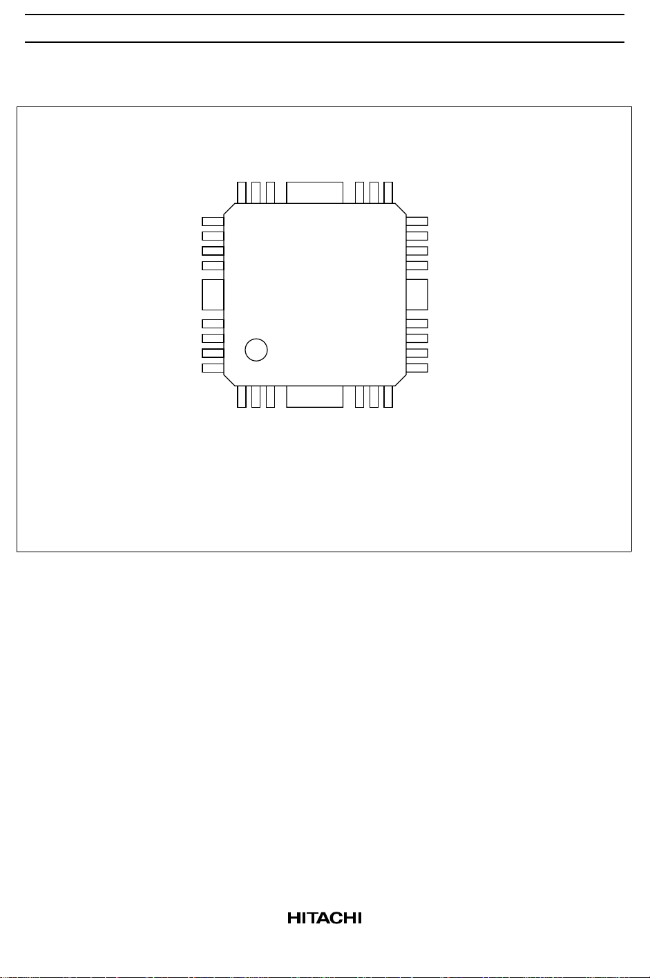
Pin Arrangement
CC
U(–)input
U(+)input
V
Hall bias
Bias(–)pin
Bias(+)pin
V(+)input
V(–)input
W(+)input
W(–)input
AGC
NC
NC
FG(+)input
18
19
20
21
22
23
24
TAB
25
26
27
28
123
FG(–)input
RPM control pin
TAB
TAB
Index PC
(Top view)
16 15
17
TAB
456
Index TC
Index output
14
13
12
11
10
9
8
7
CEB
Bias output
U phase output
V phase output
Current detection
W phase output
Phase compensation
Charge pump output
CLK input
2
Page 3

HA13565F
Pin Function
Pin No. Pin Name Function
1 FG (–) input FG amp. (–) input terminal
2 RPM control pin Control terminal for motor rotation speed
“H” → 360 rpm, “L” → 300 rpm
3 Index PC Connection for the time constant circuit that adjusts the index circuit Vth
level.
4 Index TC Burst setting time constant circuit for index circuit
5 Index output Index signal output terminal (Open collector)
6 CEB Chip enable terminal “H”: disable, “L”: enable
7 CLK input Reference clock input terminal
8 Charge pump output Connection for the time constant circuit that integrates the speed error
signal.
9 Phase compensation Connection for the phase compensation capacitor that stabilizes the
operation of the control system.
10 W phase output W phase output
11 Current detection Output current detection and terminal which is connected with resistor
for current limiter.
12 V phase output V phase output
13 U phase output U phase output
14 Bias output Smoothing circuit for the pumped output circuit
15 Bias (+) pin Output circuit used for bias pumping
16 Bias (–) pin Input circuit used for bias pumping
17 Hall bias Hall element bias input
18 V
19 U phase (+) input U phase (+) input terminal
20 U phase (–) input U phase (–) input terminal
21 V phase (+) input V phase (+) input terminal
22 V phase (–) input V phase (–) input terminal
23 W phase (+) input W phase (+) input terminal
24 W phase (–) input W phase (–) input terminal
25 AGC Smoothing circuit for hall amplifier output amplitude control
26 NC No connection
27 NC No connection
28 FG (–) input Index amp (+) input terminal
CC
Power supply
3
Page 4
HA13565F
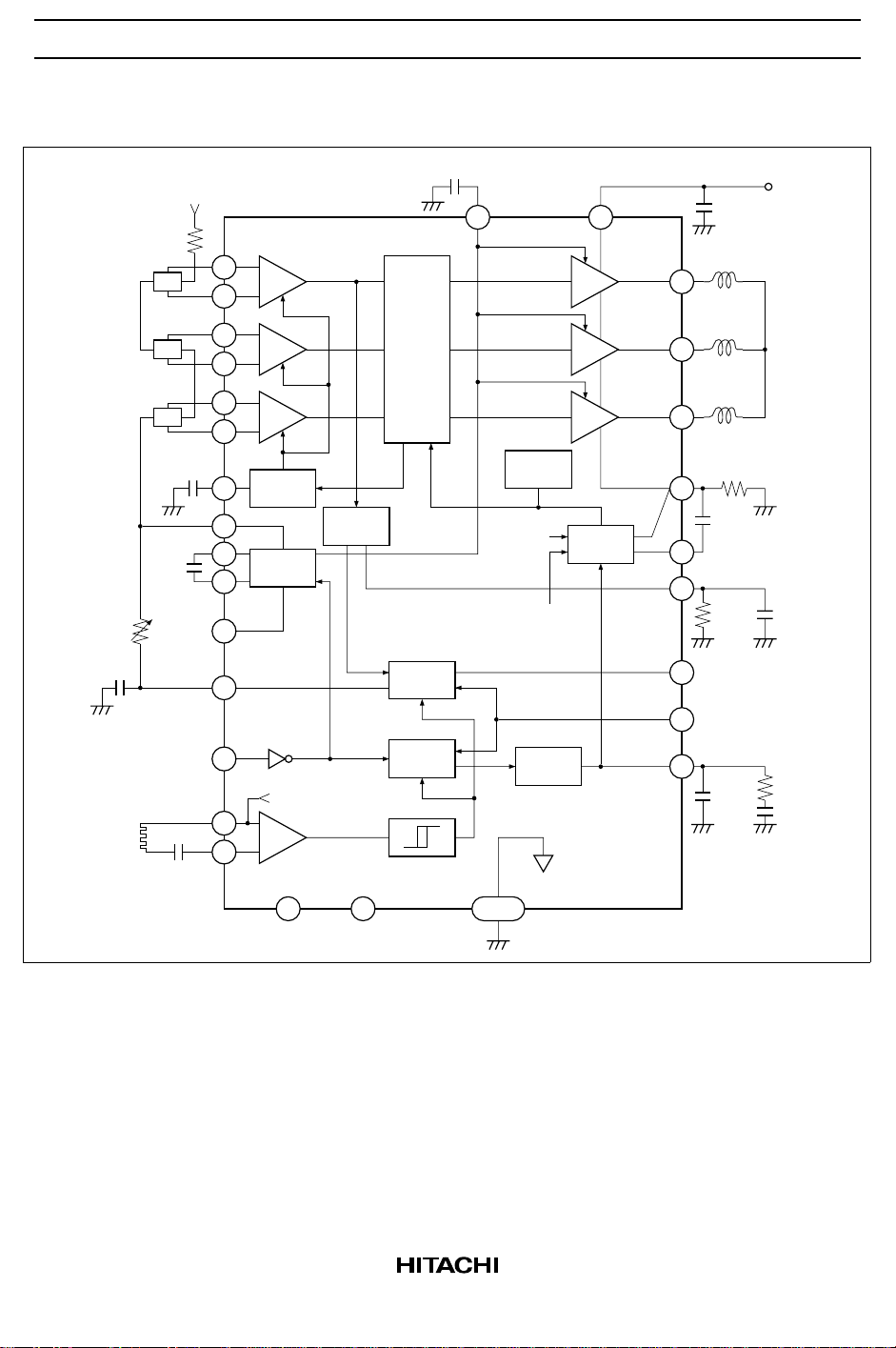
Block Diagram
Rt2
Ct2
FG
60ppr
R101
Hu
Hv
Hw
C104
C103
V
CC
C102
CLK
1MHz
19
20
21
22
23
24
25
17
16
15
28
C105
1814
+
u
–
+
v
–
+
w
–
AGC
Index
detection
Bias
6CEB
4
7
1.6V
+
–
1
FG amp.
Soft
switch
matrix
Time
constant
Discrim-
inator
OTSD
Vref1
0.175V
0.63V
Charge
pump
U
V
W
Current
control
Vref2
C101
13
12
10
11
C106
9
3
5 INDEX output
RPM select
2
H : 360rpm
L : 300rpm
8
C1
Rnf
V
Ct1Rt1
R2
C2
CC
27
NC
26 TAB
NC
4
Page 5
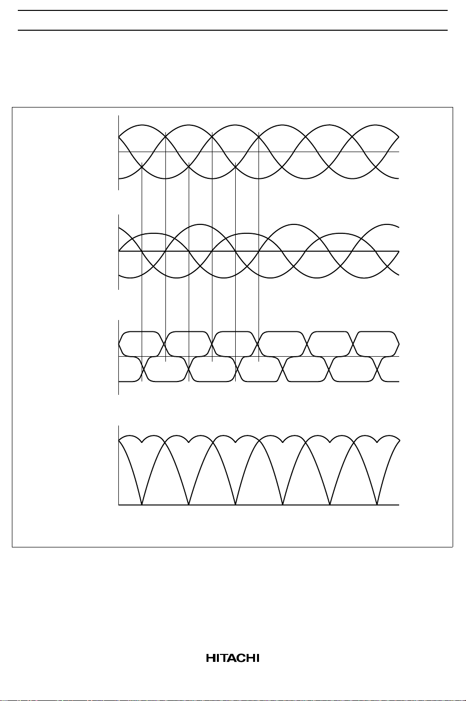
Timing Chart
Hall Amp. Input vs. Output Voltage and Current
HA13565F
B-EMF
Hall amp.
input
Output
current
U
+
0
–
U
+
0
–
UVW
+
0
–
VW
VW
UVW
Output
voltage
0
Note: 1. The input waveforms to the hall amp. should be sine waves with a third harmonic content
of less than 20%.
5
Page 6
HA13565F
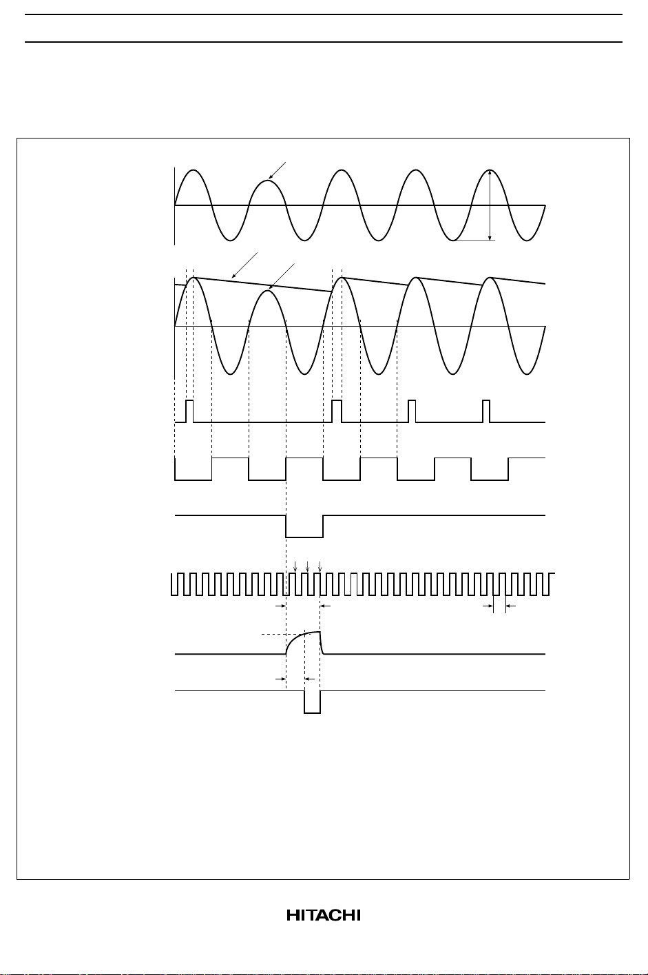
Input Detection Timing
RPM Control Pin = L
U phase hall
amp. input
Pin 19–Pin 20
Index detection
input
Index detection
output-1 *
Index detection
output-2 *
Index detection
output-3 *
2
2
2
Magnetization reduced
by 30% *
1
65 to 200mVpp
+
0
–
Pin 3
Hall amp. output *
2
+
0
–
0
0
0
FG amp.
2
output *
Index TC
Pin 4
0
6.67 to 10ms
(@300rpm) *
3
3.33ms
(@300rpm)
Vth2L
0
Burst adjustment
Index output
Pin 5
Note: 1.
To generate the index output, one pole of the main magnetization must be reduced so that
0
a difference of at least 30% is assured at the Hall amp. input.
These waveforms are shown to indicate the principles of operation, and are not actual
2.
measured waveforms.
Burst adjustment is started by the fall of the index detector output 3, and then, it ends by
3.
the third of fall of FG amp. output.
Incorrect pulses may be output immediately after (i.e., within about 200ms of) start-up.
4.
If the reduction in the magnetization is inadequate, the index signal may not be generated.
5.
Also note that excessive modulation of the Hall amp. input can cause incorrect pulses to be
generated.
6
Page 7

HA13565F
External Parts
Part No. Recommended Value Purpose Notes
R2 — Integration constant 1
R101 — Hall bias
Rnf 0.33Ω Spindle current detection and current limitation 2
Rt1 1MΩ Index circuit Vth adjustment
Rt2 — Index burst adjustment 5
C1, C2 — Integration constants 1
C101 ≥0.1µF Power supply bypass 3
C102 0.047µF AGC filter 4
C103 0.47µF FG amp. AC coupling
C104 ≥0.1µF Bias pumping
C105 ≥0.1µF Smoothing for bias pumping 6
C106 0.1µF Control amp. phase compensation
Ct1 0.1µF Index circuit Vth adjustment
Ct2 — Index burst adjustment 5
Notes: 1. Use the following formulas as a design target when determining the integration constants for
actual systems.
2π f
ω
O
R2 = (Ω)
C1 = (F)
FG
≤ (rad/S)
20
1
J ωO NO Rnf
9.55
Gctl Icp
K
T
1
101ω
R2
O
C2 = 10 C1 (F)
where,
w
: Time constant of servo loop
O
f
: FG frequency (Hz)
FG
N
: Motor speed (rpm)
O
J : Motor moment of inertia (kg · cm · s)
K
: Motor torque constant (kg · cm / A)
T
Rnf : Current detection resistance (Ω)
Gctl : Control gain (see Electrical Characteristics)
Icp : Charge pump output current (see Electrical Characteristics)
2. The current limiter operates according to the following formula.
I
OMAX
Vref1
=
Rnf
(A)
where, Vref1 is the current limiter reference voltage (see Electrical Characteristics)
7
Page 8

HA13565F
3. Place as close to the IC as possible.
4. Determine C102 according to the following formulas.
C102 ≥ (µF)
C103 ≥ (µF)
where,
P = Number of motor poles
5. The burst time t1 is defined as follows. (see Electrical Characteristics)
t1
H
t1
L
where, Rt2 is resistance inter pin 4 and pin 17.
6. If the circuit is affected by noise, a large capacitance value should be set.
200
N
· P
O
100
f
FG
= –Ct2 × Rt2 × ln (1 – Vth2H / Vhb)
= –Ct2 × Rt2 × ln (1 – Vth2L / Vhb)
8
Page 9

HA13565F
Absolute Maximum Ratings (Ta = 25°C)
Item Symbol Value Unit Notes
Power supply voltage V
CC
Peak output current Iop 1.0 A
Normal output current Io 0.7 A
Input voltage Vi 0 to VCC + 0.3 V 2
Power dissipation P
T
Junction temperature Tj +150 °C1
Storage temperature range Tstg –55 to +125 °C
Notes: 1. The operating range is as follows.
V
= 4.25 to 6.5 V
CC
Tjop = 0 to +125°C
2. Applied to the logic input pin.
3. Permissible value when Tpin = 113°C and thermal resistance is as follows:
θj-pin ≤ 25°C/W
θj-a1 ≤ 55°C/W (when mounted on a metal substrate)
θj-a2 ≤ 80°C/W (when mounted on a glass epoxy substrate)
7.0 V 1
1.5 W 3
9
Page 10

HA13565F
CC
Electrical Characteristics (VCC = 5V, Ta = 25°C)
Item Symbol Min Typ Max Unit
Quiscent current I
Logic
input
Input
current
I
I
CCO
CC
CEB
— — 0.45 mA CEB=H,
— 9 13 mA CEB=L,
——±80 µAV
(Pin 6)
Input
I
RPM
——±100 µAV
current
(Pin 2)
Input
I
CLK
——±320 µA Vclk=0 to 5V 7
current
(Pin 7)
Input low
V
IL
— — 0.8 V 2, 6, 7
voltage
Input high
V
IH
2.0 — — V
voltage
Index
output
Output
low
V
OL
— — 0.4 V Io=2mA 5
voltage
Leakage
I
OH
——±10 µA V=7.0V
current
Hall
amp.
Input
resistance
Commonmode
Rhi — 10 — kΩ 19 to 24
Vh 2.0 — V
–
V
0.5
input
voltage
Differential
vh 65 — 200 mVpp
input
voltage
Index
Vth1 80 — 90 %
detection
threshold
Output
amp.
Leakage
current
I
CER
–0.1 — 5 mA Vo=7.0V 10, 12, 13
–0.1 — 0.1 mA Vo=0V
Saturation
Vsat1 — 1.15 1.65 V Io=0.7A 1
voltage
Vsat2 — 0.6 0.85 V Io=0.35A
Test
conditions
V
=6.5V
CC
V
=6.5V
CC
=0 to 5V 6
CEB
=0 to 5V 2
RPM
Applicable
Pins Note
18
10
Page 11

Electrical Characteristics (VCC = 5V, Ta = 25°C) (cont)
HA13565F
Item Symbol Min Typ Max Unit
FG amp. Input
voltage
range
Noise
margin
Speed
discriminator
and
charge
pump
Current
control
Index
circuit
Number of
counts
Operating
frequency
Leakage
current
Output
current
Threshold
voltage
Voltage
gain
Current
limitter
voltage
Index TC
input
threshold
voltage
Index TC
Input
current
vfg 2 — 20 mVpp 1, 28
nd — — 0.5 mVpp Differential
nc — — 0.5 Vpp Common
N — 1666.5 — — RPM control
— 1388.5 — — RPM control
f
CLK
Ioff — — ±50 nA V8=0.8V 8
Icp+ — 10 — µA Speed
Icp– — –10 — µA Acceleration
Vref2 — 0.63 — V (Control start
Gctl — –10 — dB 11
Vref1 157 175 193 mV (Rnf=0.33Ω)
Vth2L — 0.65 ×
Vth2H — 0.58 ×
Itc — — ±2 µA
0.9 1.0 1.1 MHz 7
— V RPM control
Vhb
— V RPM control
Vhb
Test
conditions
noise
noise
pin=L
pin=H
reduction full
scale
full scale
voltage)
pin=L
pin=H
Applicable
Pins Note
82
43
11
Page 12

HA13565F
Electrical Characteristics (VCC = 5V, Ta = 25°C) (cont)
Item Symbol Min Typ Max Unit
Hall bias Output
voltage
Leakage
current
OTSD Operating
temperature
Hysteresis Thys — 25 — °C
Notes: 1. Total of sink and source.
2. Refer to the figure 1. Gctl = ∆Vrnf / ∆vcp.
vhb 1.9 2.2 2.5 V Ih=10mA,
Ihoff — — ±10 µA CEB=H,
Tsd 125 150 — °C4
Vrnf
Vref1
∆Vrnf
10mV
0
∆Vcp
Vref2 Vcp
Figure 1
Test
conditions
CEB=L
Vh=7.0V,
V
=7.0V
CC
Applicable
Pins Note
17
3. Refer to the timing chart.
4. At the delivery, this characteristics is not tested.
12
Page 13

Characteristics Data
(mA)
CC
Quiescent Current I
HA13565F
Quiescent Current vs. Power Supply Voltage
20
16
12
TBD
8
4
0
2845673
Power Supply Voltage VCC (V)
Disenable Quiescent Current vs. Power Supply Voltage
1.0
0.8
(mA)
CCO
0.6
0.4
0.2
Disenable Quiescent Current I
0
2845673
Power Supply Voltage VCC (V)
TBD
13
Page 14

HA13565F
Output Saturation Voltage vs. Output Current
2.0
1.6
1.2
TBD
0.8
0.4
Output Saturation Voltage VsatH & VsatL (V)
0
0 1.00.2 0.4 0.6 0.8
Output Current IO (A)
Current Limiter Voltage vs. Rnf
200
190
180
TBD
170
Current Limiter Voltage Vrnf (V)
160
150
0.2 1.20.4 0.6 0.8 1.0
Rnf (Ω)
14
Page 15

Hall Bias Voltage vs. Hall Bias Current
2.5
2.0
1.5
TBD
1.0
Hall Bias Voltage Vhb (V)
0.5
0
0204 8 12 16
Hall Bias Current Ih (mA)
HA13565F
Current limiter Voltage vs. Junction Temperature
200
190
180
TBD
170
Current limiter Voltage Vrnf (V)
160
150
0 12525 50 75 100
Junction Temperature Tj (°C)
15
Page 16

HA13565F
Package Dimensions
9.0 ± 0.2
0.32 ± 0.08
0.30 ± 0.06
9.0 ± 0.2
7.0
20 15
0.65
21
28
1
0.575 0.575
14
7
6
M
0.13
1.40
1.7 Max
0.17 ± 0.05
0.15 ± 0.04
Unit: mm
1.0
0 – 8°
2.25 ± 0.1
0.10
+ 0.09
– 0.05
0.13
0.95 ± 0.10
0.50 ± 0.10
Hitachi Code
JEDEC Code
EIAJ Code
Weight
FP-28TB
—
—
0.19 g
16
Page 17

Cautions
1. Hitachi neither warrants nor grants licenses of any rights of Hitachi’s or any third party’s patent,
copyright, trademark, or other intellectual property rights for information contained in this document.
Hitachi bears no responsibility for problems that may arise with third party’s rights, including
intellectual property rights, in connection with use of the information contained in this document.
2. Products and product specifications may be subject to change without notice. Confirm that you have
received the latest product standards or specifications before final design, purchase or use.
3. Hitachi makes every attempt to ensure that its products are of high quality and reliability. However,
contact Hitachi’s sales office before using the product in an application that demands especially high
quality and reliability or where its failure or malfunction may directly threaten human life or cause risk
of bodily injury, such as aerospace, aeronautics, nuclear power, combustion control, transportation,
traffic, safety equipment or medical equipment for life support.
4. Design your application so that the product is used within the ranges guaranteed by Hitachi particularly
for maximum rating, operating supply voltage range, heat radiation characteristics, installation
conditions and other characteristics. Hitachi bears no responsibility for failure or damage when used
beyond the guaranteed ranges. Even within the guaranteed ranges, consider normally foreseeable
failure rates or failure modes in semiconductor devices and employ systemic measures such as failsafes, so that the equipment incorporating Hitachi product does not cause bodily injury, fire or other
consequential damage due to operation of the Hitachi product.
5. This product is not designed to be radiation resistant.
6. No one is permitted to reproduce or duplicate, in any form, the whole or part of this document without
written approval from Hitachi.
7. Contact Hitachi’s sales office for any questions regarding this document or Hitachi semiconductor
products.
Hitachi, Ltd.
Semiconductor & Integrated Circuits.
Nippon Bldg., 2-6-2, Ohte-machi, Chiyoda-ku, Tokyo 100-0004, Japan
Tel: Tokyo (03) 3270-2111 Fax: (03) 3270-5109
URL NorthAmerica : http:semiconductor.hitachi.com/
For further information write to:
Hitachi Semiconductor
(America) Inc.
179 East Tasman Drive,
San Jose,CA 95134
Tel: <1> (408) 433-1990
Fax: <1>(408) 433-0223
Europe : http://www.hitachi-eu.com/hel/ecg
Asia (Singapore) : http://www.has.hitachi.com.sg/grp3/sicd/index.htm
Asia (Taiwan) : http://www.hitachi.com.tw/E/Product/SICD_Frame.htm
Asia (HongKong) : http://www.hitachi.com.hk/eng/bo/grp3/index.htm
Japan : http://www.hitachi.co.jp/Sicd/indx.htm
Hitachi Europe GmbH
Electronic components Group
Dornacher Stra§e 3
D-85622 Feldkirchen, Munich
Germany
Tel: <49> (89) 9 9180-0
Fax: <49> (89) 9 29 30 00
Hitachi Europe Ltd.
Electronic Components Group.
Whitebrook Park
Lower Cookham Road
Maidenhead
Berkshire SL6 8YA, United Kingdom
Tel: <44> (1628) 585000
Fax: <44> (1628) 778322
Hitachi Asia Pte. Ltd.
16 Collyer Quay #20-00
Hitachi Tower
Singapore 049318
Tel: 535-2100
Fax: 535-1533
Hitachi Asia Ltd.
Taipei Branch Office
3F, Hung Kuo Building. No.167,
Tun-Hwa North Road, Taipei (105)
Tel: <886> (2) 2718-3666
Fax: <886> (2) 2718-8180
Copyright ' Hitachi, Ltd., 1999. All rights reserved. Printed in Japan.
Hitachi Asia (Hong Kong) Ltd.
Group III (Electronic Components)
7/F., North Tower, World Finance Centre,
Harbour City, Canton Road, Tsim Sha Tsui,
Kowloon, Hong Kong
Tel: <852> (2) 735 9218
Fax: <852> (2) 730 0281
Telex: 40815 HITEC HX
 Loading...