

Page 1

HA13561F
Combo (Spindle & VCM) Driver
ADE-207-182 (Z)
1st Edition
July 1996
Description
This COMBO Driver for HDD application consists of Sensorless Spindle Driver and BTL type VCM Driver.
Bipolar Process is applied and a “Soft Switching Circuit” for less commutation noise and a “Booster Circuit’
for smaller Saturation Voltage of Output Transistor are also implemented.
Features
• Soft Switching Driver
Small Surface Mount Package: FP-80E (QFP80 Pin)
Low thermal resistance: 35°C/W with 6 layer multi glass-epoxy board
• Low output saturation voltage
Spindle 0.8 V Typ (@1.0 A)
VCM 0.8 V Typ (@0.8 A)
Functions
• 1.8 A Max/3-phase motor driver
• 1.2 A Max BTL VCM Driver
• Auto retract
• Soft Switching Matrix
• Start up circuit
• Booster
• Speed Discriminator
• Internal Protector (OTSD, LVI)
• POR
• Power monitor
Page 2
HA13561F
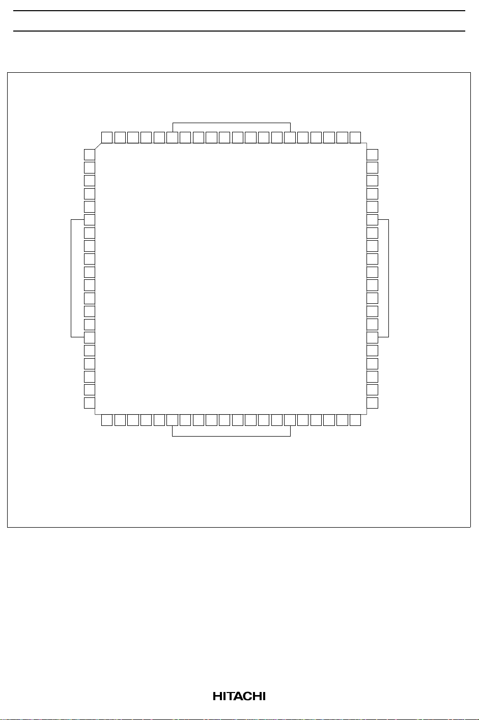
Pin Arrangement
)
+
TAB
RS
RETON
RETPOW
Vpsv
80 79 78 77 76 75 74 73 72 71 70 69 68 67 66 65 64 63 6162
LVI2
OPIN(-)
VCTL
OPIN(
RESINH
VREF1
1
VBST
BC2
BC1
W
RNF
CT
2
3
4
5
6
7
8
9
10
11
12
13
14
15
16
17
18
19
20
V
21 22 23 24 25 26 272829 30 31 32 33 34 35 36 37 38 39 40
U
R1
CLREF
C-PUMP
Vpss
TAB
VCMP
VCMN
TAB
PCOMP
*NC : No internal connection
Please note that there is no isolation check between pin 58 and pin 59
at the testing of this IC.
(Top View)
Vss
LVI1
COMM
DELAY
60
COMPOUT
59
NC*
58
NC*
57
GAIN
56
VCMENAB
55
54
53
52
51
50
49
48
47
46
45
POR
44
SPNENAB
43
READY
42
CLOCK
41
CNTSEL
POLSEL
TAB
2
Page 3

HA13561F
Pin Description
Pin Number Pin Name Function
1 VBST Boosted voltage output to realize the low output saturation voltage
2 VCMP Output terminal on VCM driver
3 VCMN Output terminal on VCM driver
4 BC2 To be attached the external capacitor for booster circuitry
5 BC1 ditto
6 to 15 GND Ground pins
16 W W phase output terminal on spindle motor driver
17 RNF Sensing input for output current on spindle motor driver
18 PCOMP To be attached the external capacitor for phase compensation of spindle
motor driver
19 CT To be attached the center tap of the spindle motor for B-EMF sensing
20 V V phase output terminal on spindle motor driver
21 U U phase output terminal on spindle motor driver
22 C-PUMP To be attached the external integral constants for speed control of spindle
motor
23 CLREF Reference voltage input for current limiter of spindle motor driver
24 R1 To be attached the external resistor for setting up the oscillation frequency of
start-up circuitry and the gain of speed control loop of spindle motor driver
25 Vpss Power supply for spindle motor driver
26 to 35 GND Ground pins
36 V
37 LVI1 Sensing input for power monitor circuitry
38 DELAY To be attached the external capacitor to generate the delay time for power on
39 COMM To be attached the external capacitor for setting up the oscillation frequency
40 POLSEL To be selected the input status corresponding to the pole number of spindle
41 CNTSEL To select the count Number of Speed Discriminator
42 CLOCK Master clock input for this IC
43 READY Output of speed lock detector for spindle motor
44 SPNENAB To select the status of spindle motor driver
45 POR Output of power on reset signal for HDD system
46 to 55 GND Ground pins
56 VCMENAB To select the status of VCM driver
57 GAIN To select the Transfer conductance gm of VCM driver
SS
Power supply for small signal block
reset signal
motor
3
Page 4

HA13561F
Pin Description (cont)
Pin Number Pin Name Function
58 NC No function
59 NC ditto
60 COMPOUT Comparator output to detect the direction of output current on VCM driver
61 VREF1 Regulated voltage output to be used as reference of peripheral ICs
62 RESINH Used for inhibiting the restart function of the spindle motor driver after power
down
63 OPIN (+) Non inverted input of OP.Amp. to be used for filtering the signal on PWMOUT
64 VCTL OP. Amp. output, this signal is used as control signal for VCM driver output
65 OPIN (–) Inverted input of OP.Amp. to be used for filtering the signal on PWMOUT
66 to 75 GND Ground pins
76 LVI2 Sensing input for power monitor circuitry
77 Vpsv Power supply for VCM driver
78 RETPOW Power supply for retract circuitry
79 RETON To be attached the base terminal of external transistor for retracting
80 RS Sensing input for output current on VCM driver
4
Page 5

Block Diagram
HA13561F
RESINH
COMM
C103
C-PUMP
C2
C1
CLREF
R1b
SPNENAB
POLSEL
CLOCK
(5MHz Typ)
CNTSEL
READY
VCTL
OPIN(–)
OPIN(+)
Vref1
GAIN
VCM ENAB
C104
C105
R1
R1a
NC
NC
BC1
BC2
V
VSS (+5V)
V
SS
36 25
C102
B-EMF
AMP.
SOFT
SWITCHING
MATRIX
62
39
START-UP
CIRCUIT
COMMUTATION
LOGIC
22
23
CHARGE
PUMP
CURRENT
CONTROL
24
44
40
(D1)
SPEED DISCRI.
42
1/32
(CNT)
41
43
SPEED
READY
V
BST
64
–
65
63
61
59
58
+
OPAMP.
Vref1
(=4.6V)
OTSD
+
VCM
DRIVER
–
57
56
5
4
1
BST
BOOSTER
Vss
(+5V)
V
BST
Vss
37 76 38
LVI1
R101
POWER
MONITOR
LVI2
R103
Vps
R102 R104
Vps
(+12V)
POR
Delay
DELAY
C106
V
BST
Vpss
SPINDLE
DRIVER
RETRACT
DRIVER
P
N
COMPARATOR
Vps(+12V)
U
V
W
PCOMP
Vpsv
RETPOW
RETON
VCMP
VCMN
–
+
GND
6 to 15,26 to 35
46 to 55,66 to 75
C101
CT
19
21
U
20
V
16
W
17
18
77
78
79
2
3
80
RS
COMP
60
OUT
R105
45
POR
(L:RESET)
R
C110
C111
D1
R108
C
R
NF
Qret
X
X
Vss(+5V)
C109
R
S
R
L
D2
5
Page 6

HA13561F
Truth Table
Table 1 Truth Table (1)
SPNENAB Spindle Driver
HON
Open Cut off
L Braking
Table 2 Truth Table (2)
VCMENAB VCM Driver
HON
L Cut off
Table 3 Truth Table (3)
OTSD Spindle Driver VCM Driver Retract Driver
not Active See table 1 See table 2 Cut off
Active Cut off Cut off ON
Table 4 Truth Table (4)
POLSEL (D1) Comment
H — Test Mode
Open 1/12 for 8 poles motor
L 1/18 for 12 poles motor
Table 5 Truth Table (5)
Rotation Speed
CNTSEL CNT
H 2605 3,600 rpm
Open 2084 4,500 rpm
L 1736 5,400 rpm
(at CLOCK = 5 MHz)
6
Page 7

Table 6 Truth Table (6)
RESINH Spindle Driver
H Inhibiting the restart after power down
L Not inhibiting the restart after power down
Table 7 Truth Table (7)
GAIN VCM Driver
H High Gain Mode
L Low Gain Mode
HA13561F
7
Page 8
HA13561F
Timing Chart
1. Power on reset (1)
Vsd
Vps and
V
SS
Vhys
t
POR
1.0V
MAX
0
t
DLY
Note: 1. How to determine the threshold Voltage Vsd and the delay time t
external components table.
2. Power on reset (2)
VPS or
V
SS
POR
Spindle
Driver
ON
OFF
t
por
t
por
<1µs <1µs
t
both are shown in the
DLY
VCM
Driver
Retract
Driver
ON
OFF
Note: 2. Retract driver need B-EMF voltage or another power supply.
8
Retract
Page 9

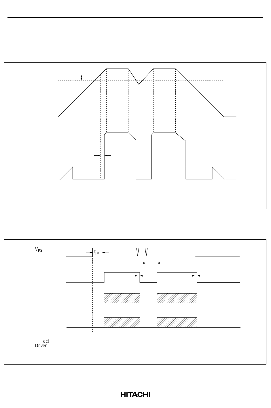
3. Motor start-up seaquence
,
(a) Timing chart of start-up seaquence
SPNENAB
HA13561F
Open
No
Rotation
Speed
Synchronous
Driving
Driving by
B-EMF
sensing
0
Internal
READY
READY
(Pin 43)
Switching
t
delay
2
*
Note *1. Speed lock detection range ∆No is as follows.
∆No=1.2% when CNTSEL=H
=1.5% when CNTSEL=Open
=1.8% when CNTSEL=L
*2. READY output goes to High, if the rotation speed error keeps to be less than
∆No longer time than tdelay.
7
tdelay= [ms]
500 • 10
fclk [Hz]
*3. The turning point of driving mode from switching synchronize to the turning
point of READY output from Low to High.
Soft Switching*
3
t
No+∆No*
No–∆No*
1
1
(b) Retry circuitry for misstart-up
Motor
on
Synchronous
driving
Driving by
B-EMF
sensing
(not stop)
Motor
stop
detector
(Motor stop)
(Motor off)
The HA13561F has the motor stop detector as shown hatching block. This function is monitoring the
situation of the motor while the motor is running by B-EMF sensing. If the motor will be caused a
misstarting up, the motor will be automatically restarted within 200 ms after the motor stopped. This
function increase the reliability for the motor starting up.
9
Page 10

HA13561F
4. Braking & Shut down the Spindle Driver
Open
Open
SPNENAB
> 20µs
ON CUT OFF BRAKING CUT OFF
Note: The SPNENAB should be selected the open state after braking to reduce the supply current from Vps
and VSS.
5. Start-up of the Spindle motor
Open
SPNENAB
COMM
SOURCE
I
U
GND
SINK
t
(see External Components Table)
COMM
Vth1
Vth2
0
SOURCE
I
V
SOURCE
I
W
0
SINK
0
SINK
COMM4TCOMM4TCOMM4TCOMM4TCOMM4TCOMM6TCOMM8TCOMM
2T
not detecting the B-EMF detecting the B-EMF
COMM
10T
COMM
12T
COMM
14T
COMM
16T
Synchronous Driving for motor start up
10
COMM
Driving by
B-EMF sensing
16T
Page 11

6. Acceleration and Running the spindle motor
+
U
BEMF
V
BEMF
W
BEMF
(1) Acceleration(switching mode)
SOURCE
Iu
SOURCE
Iv
SOURCE
Iw
0
–
+
0
–
+
0
–
0
SINK
0
SINK
0
SINK
HA13561F
(2) Running (soft switching mode)
SOURCE
Iu
SOURCE
Iv
SOURCE
Iw
0
SINK
0
SINK
0
SINK
11
Page 12

HA13561F
Application
RWMIN
V
SS
(+5V)
R101
R102
R8
R7
R3
C104
C105
C103
R1aR1b
C2 R2
C1
R5
C5
C3
R4
C102
R105
5
4
1
39
23
24
22
40
41
43
42
44
56
57
62
61
65
R6
64
63
C4
60
36
45
38
BC1
BC2
VBST
COMM
CLREF
R1
HA13561F
C-PUMP
POLSEL
CNTSEL
READY
CLOCK
SPNENAB
VCMENAB
GAIN
RESINH
VREF1
OPIN(–)
VCTL
OPIN(+)
COMPOUT
V
SS
POR
DELAY
GND
Vpss
CT
RNF
PCOMP
Vpsv
RETPOW
RETON
VCMP
VCMN
RS
LVl2
LVl1
W
V
PS
(+12V)
25
C101
19
U
21
V
20
16
R
NF
17
C110
18
C111
77
C109
R103
78
D2
79
Qret
R104
D1
R108
2
R
S
3
C
X
R
X
RL
80
76
37
C106
12
Page 13

HA13561F
External Components
Parts No. Recommended Value Purpose Note
R1a (R1a + R1b) ≥ 10 kΩ V/I converter 1, 4, 6
R1b (R1a + R1b) ≥ 10 kΩ
R2 — Integral constant 3
R3 to R8 — PWM filter 9
R101, R102 — Setting of LVI1 voltage 7
R103, R104 — Setting of LVI2 voltage 7
R105 5.6 kΩ Pull up
R108 — Limitation for Retract current 12
RS 1.0 Ω Current sensing for VCM Driver 10
Rnf — Current sensing for Spindle Driver 1
R
X
C1, C2 — Integral constant 3
C3 to C6 — PWM filter 9
C
X
C101 ≥ 0.1 µF Power supply by passing
C102 ≥ 0.1 µF Power supply by passing
C103 — Oscillation for start-up 6
C104 0.22 µF for booster
C105 2.2 µF for booster
C106 — Delay for POR 8
C109 ≥ 0.1 µF Power supply by passing
C110, C111 0.33 µF Phase compensation
Qret — Retract Driver 12
D1 — Protection for Qret 12
D2 TBD Protection for parasitic phenomena
Notes: 1. Output maximum current on spindle motor driver Ispnmax is determined by following equation.
Ispnmax = [A]•
— Reduction for gain peaking 11
— Reduction for gain peaking 11
R1b
R1a + R1b
V
R1
R
NF
(1)
where, V
: Reference Voltage on Pin 24 [V] (= 1.3)
R1
2. Input clock frequency fclk on pin 42 is determined by following equation.
4
fclk = • N
where, N
• P • D1 • (CNT – 0.5) [Hz]
O
5
: Standard rotation speed [rpm]
O
P: Number of pole
D1: Dividing ratio on divider 1
13
(2)
Page 14

HA13561F
3. Integral constants R2, C1 and C2 can be designed as follows.
ω
= [rad/s]• 2 • π •
O
R2 = [Ω]•
D1 = 1/12 (when Pin 40 = Open) for 8 pole motor
= 1/18 (when Pin 40 = Low) for 12 pole motor
CNT:Count number on speed discriminator
CNT= 2605 (when Pin 41 = High)
= 2084 (when Pin 41 = Open)
= 1736 (when Pin 41 = Low)
1
10
1
9.55
N
O
60
Rnf • J • ωO • NO • (R1a + R1b)
V
• KT • Gctl
R1
(3)
(4)
C1 = [F]
C2 = 10 • C1 [F]
where, J: Moment of inertia [kg•cm•s
1
10 • ω
• R2
O
K
: Torque constant [kg•cm/A]
T
(5)
(6)
2
]
Gctl: Current control amp gain from pin 22 to pin 17 (= 0.5)
4. It is notice that rotation speed error Nerror is caused by leak current Icer2 on pin 22 and this error
depend on R1a and R1b as following equation.
Nerror = Icer2 • [%]• 100
(R1a + R1b)
VR1
(7)
where, Icer2: Ieak current on pin 22 [A]
5. Oscillation period t
on pin 39 which period determine the start up characteristics, is should be
COMM
chosen as following equation.
t
COMM
1
= • [s]to
8
P • K
J
• Ispnmax
T
6. The capacitor C103 on pin 39 can be determined by t
C103 = • [F]
1
4
where, Vth
VR1
R1a + R1b
: Threshold voltage on start up circuit [V] (= 2.0)
H
Vth
: Threshold voltage on start up circuit [V] (= 0.5)
L
t
COMM
•
VthH – Vth
1
•
4
L
P • K
J
• Ispnmax
T
and following equation.
COMM
(8)
(9)
7. LVI operatig voltage Vsd1, Vsd2 and its hysteresis voltage Vhys1, Vhys2 can be determined by
following equations.
for V
SS
Vsd1 = 1 + • Vth4 [V]
R101
R102
(10)
Vhys1 = 1 + • Vhyspm [V]
R101
R102
(11)
14
Page 15

for Vps
Vsd2 = 1 + • Vth3 [V]
R103
R104
HA13561F
(12)
Vhys2 = 1 + • Vhyspm [V]
R103
R104
(13)
where, Vth3, Vth4: Threshold voltage on pin 37 and pin 76 [V] (= 1.39)
Vhyspm: Hysteresis voltage on pin 37 and pin 76 [mV] (= 40)
Shut down voltage Vsd1, Vsd2 can be designed by the following range.
Vsd1 ≥ 4.25 [V], Vsd2 ≥ 10 [V]
8. The delay time t
C106 • Vth5
t
= [s]
DLY
I
CH3
of POR for power on reset is determined as follows.
DLY
(14)
where, Vth4: Threshold voltage on pin 38 [V] (= 1.4)
I
: Charge current on pin 38 [µA] (= 10)
CH3
9. The differential voltage (Vctl – V
) using for control of VCM driver depend on PWMDAC inputs
REF1
LSB, MSB as follows.
Vctl – V
REF1
where, D
– 50
PWM
•
100
H
= 2 • V
PWM
FLT(S)
REF1
: Duty cycle on PWMIN [%]
: Transfer function from pin 62 (PWMOUT) to pin 64 (Vctl) as shown in equation
R6
•• H
R5
FLT
(s)
(15)
D
(17)
To be satisfied with above equation (15), it is notice that the ratio of R6 to R7 must be choosen as
shown below.
R8
R7
= 2 •
R6
R5
1
•
R6
1 –
R5
(16)
H
(s)
FLT
=
1 + s • C5 • R// – C3 • (R// + R3) • + C4 • (R// + R3 + R4)
+ s2 • C5 • C4 • R// • (R3 + R4) – C5 • C3 • R// • R3 • + C3 • C4 • R4 • (R// + R3)
3
• C3 • C4 • C5 • R// • R3 • R4
+ s
R7 • R8
R// =
where,
R7 • R8
1
R6
R5
R6
R5
If you choose the R// << R3, then equation (17) can be simplified as following equation.
H
(s) =
FLT
1 +
1
•
s
1 +2 • ζ •
ω
O
1
s
ωn
2
s
+
ωn
15
(17)
(18)
(19)
Page 16

HA13561F
where,
ωO =
1
C5 • R//
(20)
ωn =
1
C3 • C4 • R3 • R4
C4 • (R3 + R4) – C3 • R3 •
ζ =
R6
R5
2 • C3 • C4 • R3 • R4
10.The relationship between the output current Ivcm and the input voltage (Vctl – V
is as follows.
Ivcm(s) = Vctl – V
REF1
• Kvcm •
1
Rs
• Hvcm(s)
where, Vctl: Input control voltage for VCM driver on pin 64 [V]
V
: Reference voltage on pin 61 [V] (= 4.6)
REF1
Kvcm: DC gain of VCM driver
(= 1.82 for High gain mode)
(= 0.45 for Low gain mode)
Hvcm(s): Transfer function of VCM driver as shown following equation
VCM
1
ω
s
VCM
2
s
•
ω
VCM
+
Hvcm(s) =
1 + 2 • ζ
where,
ω
VCM
= ωP•
Rs
Lm
(21)
(22)
) on VCM driver
REF1
(23)
(24)
(25)
1
ζ
= •1 +
VCM
1
2
R
Rs
L
•
ω
Rs
•
Lm
P
where, ωp: Bandwidth of internal power amplifiers for VCM driver [rad/s]
(= 3•π•10
6
)
Lm: Inductance of the VCM coil [H]
R
: Resistance of the VCM coil [Ω]
L
and from above equations the -3 dB bandwidth f
ω
f
VCMC
VCM
= • 1 – 2 • ζ
2 • π
VCM
2
+ 2 • ζ
of VCM driver is as following equation.
VCMC
2
– 12+ 1
VCM
16
(26)
(27)
Page 17

HA13561F
11.The frequency response of VCM driver maybe have a gain peaking because of the resonation of
the motor coil impedance. If you want to tune up for this characteristics, you can reduce the
peaking by additional snubber circuit R
and CX as follows.
X
BTL Driver
+
–
R3
R3
–
1/2 V
PS
+
Figure 1 VCM Driver Block Diagram
20
10
Normal
0
I
O
(dB)
–10
–20
C
= 0.22µF
X
RX = 560Ω
N
RS
P
R
X
Coil
C
X
R
S
100 1k 10k 100k
Frequency (Hz)
(for example) RL = 14.7 Ω, RS = 1 Ω, L = 1.7 mH, Gain = L
12.The retract current Iret is determined by following equation.
Vretpow – Vsat(Qret) – V
Iret =
R108 + Rs + R
(D1) – Vsat
F
L
VL
where, Vretpow: Applied voltage on pin 78 [V]
Vsat (Qret): Saturation voltage of Qret [V]
V
(D1): Foward voltage of D1 [V]
F
17
(28)
Page 18

HA13561F
Absolute Maximum Ratings (Ta = 25°C)
Item Symbol Rating Unit Notes
Power supply voltage Vps +15 V 1
Signal supply voltage V
Input voltage V
SS
IN
Output current-Spindle Iospn (Peak) 1.8 A
Iospn (DC) 1.2 A
Output current-VCM Iovcm (Peak) 1.2 A
Iovcm (DC) 0.8 A
Power dissipation P
T
Junction temperature Tj +150 °C
Storage temperature Tstg –55 to +125 °C
Notes: 1. Operating voltage range is 10.2 V to 13.8 V.
2. Operating voltage range is 4.25 V to 5.75 V
3. Applied to Pin 40, 41, 42, 44, 56, 57 and pin 62
4. Operating junction temperature range is Tjop = 0°C to +125°C
5. ASO of upper and lower power transistor are shown below.
Operating locus must be within the ASO.
6. The OTSD (Over Temperature Shut Down) function is built in this IC to avoid same damages by
over heat of this chip. However, please note that if the junction temperature of this IC becomes
higher than the operating maximum junction temperature (Tjopmax = 125°C), the reliability of this
IC often goes down.
7. Thermal resistance: θj-a ≤ 35°C/W with 6 layer multi glass-epoxy board.
+7 V 2
V
SS
V3
5W
10
t=10ms
1.8
1
IC (A)
0.1
1 10 100
VCE (V)
t=50ms
t=100ms
15
Figure 2 ASO of Output Stages (Spindle)
18
Page 19

10
1.2
1
IC (A)
HA13561F
t=10ms
t=50ms
t=100ms
0.1
1 10 100
15
VCE (V)
Figure 3 ASO of Output Stages (VCM)
19
Page 20

HA13561F
Electrical Characteristics (Ta = 25°C, Vps = 12 V, VSS = 5 V)
Item Symbol Min Typ Max Unit Test Conditions
Supply
current
Logic input 1
(GAIN)
(RESINH)
Logic input 2
(CLOCK)
Logic input 3
(VCMENAB)
Logic input 4
(SPNENB)
for V
SS
I
SS0
I
SS1
for Vps Ips0 — 1.7 2.2 mA SPNENAB = Open
Ips1 — 19 24 mA SPNENAB = H
Input low voltage V
Input high
IL1
V
IH1
voltage
Input low current I
Input high
IL1
I
IH1
current
Input low voltage V
Input high
IL2
V
IH2
voltage
Input low current I
Input high
IL2
I
IH2
current
Input low voltage V
Input high
IL3
V
IH3
voltage
Input low current I
Input high
IL3
I
IH3
current
Input low voltage V
Input middle
IL4
V
IM4
voltage
Input high
V
IH4
voltage
Input low current I
Input high
IL4
I
IH4
current
— 5.8 7.0 mA SPNENAB = Open
VCMENAB = L
— 21 27 mA SPNENAB = H
VCMENAB = H
VCMENAB = L
VCMENAB = H
— — 0.8 V 57, 62
2.0 — — V
——±10 µA Input = GND
——±10 µA Input = 5.0 V
— — 0.8 V 42
3.5 — — V
— –180 –260 µA Input = GND
— 230 330 µA Input = 5.0 V
— — 0.8 V 56, 59
2.0 — — V
——±10 µA Input = GND
— — 330 µA Input = 5.0 V
— — 1.0 V 44
2.0 — 3.1 V
3.9 — — V
–75 –105 –150 µA Input = GND
75 105 150 µA Input = 5.0 V
Applicable
Pins Note
36
36
25, 77
25, 77
20
Page 21

HA13561F
C
Electrical Characteristics (Ta = 25°C, Vps = 12 V, VSS = 5 V) (cont)
Applicable
Item Symbol Min Typ Max Unit Test Conditions
Logic input 4
(SPNENB)
Logic input 5
Input dead
current
Input low voltage V
I
DEAD
IL5
——±10 µA44
— — 1.0 V 40, 41
(POLSEL)
(CONTSEL)
Input middle
V
IM5
2.0 — 3.1 V
voltage
Input high
V
IH5
3.9 — — V
voltage
Input low current I
Input high
IL5
I
IH5
–38 –53 –75 µA Input = GND
38 53 75 µA Input = 5.0 V
current
Spindle
driver
Total saturation
voltage
Vsatspn — 0.8 1.1 V Ispn = 1.0 A 16, 20, 21
— — 0.5 V Ispn = 0.35 A
Saturation at
Vbreak — — 0.7 V Ibreak = 0.6 A
braking
Leak current Icer1 — — ±2.0 mA SPNENAB = Open
Current limiter
reference
V
OCL
430 480 530 mV V
LREF
R
NF
= 500 mV
= 1.0 Ω
voltage
Control amp
Gctl — –2 ±2dBRNF = 1.0 Ω 17, 22
gain
B-EMF amp. Input sensitivity Vmin — 100 — mVp-p 16, 20, 21 1
Charge
pump
Reference
voltage
Charge current I
Discharge
VR1 1.06 1.17 1.28 V R1a + R1b = 24 Ω
C-PUMP = 1.0 V
40 45 50 µA
–40 –45 –50 µA
I
CH1
DIS1
current
Leak current Icer2 — — ±50 nA
Speed discri Operating
fclk — — 8.0 MHz 42
frequency
Start up
circuit
Threshold
voltage
Charge current I
Vth
Vth
CH2
1.6 1.8 2.0 V 24, 39
H
0.3 0.5 0.7 V
L
21 23 26 µA R1 a + R 1b = 24 k Ω
COMM = 1 V
Discharge
I
DIS2
–19 –22 –25 µA
current
Pins Note
17
22, 24
21
Page 22

HA13561F
SS
C
S
S
Electrical Characteristics (Ta = 25°C, Vps = 12 V, VSS = 5 V) (cont)
Applicable
Item Symbol Min Typ Max Unit Test Conditions
READY Output high
voltage
Output low
Vohr V
—V
– 0.4
Volr — — 0.4 V IO = 1 mA
VIO = –1 mA 43
SS
voltage
VCM driver Total saturation
Vsatvcm — 0.8 1.1 V Ivcm = 0.8 A 2, 3
voltage
— 0.4 0.55 V Ivcm = 0.4 A
Output leak
Icer3 — — ±2 mA Vce = 15 V
current
Total output
offset voltage
Voff(H) — — ±20 mV V
TL
V
REF
= OP (–)
= OP (+)
Voff(L) — — ±10 mV
Output
quiescent
Vqvcm 5.6 6.0 6.4 V RL = 10 Ω
R
= 1.0 Ω
S
voltage
Total Gain
Bandwidth
B — 26 — kHz RS = 1.0 Ω,
R
= 28 Ω
L
— 50 — kHz RS = 1.0 Ω,
R
= 14 Ω
L
Transfer gain gm (H) — 1.74 ±5% A/V Higain-mode
R
= 1.0 Ω,
R
= 14 Ω
L
gm (L) — 0.44 ±5% A/V Logain-mode
R
= 1.0 Ω,
R
= 14 Ω
L
Retract driver Retpow voltage Vretpow 0.8 — — V Ireton = 0.1 mA 78
Retout sink
Ireton 5 8 — mA Vretpow = 4.0 V
current
Output leak
current
Low side
Icer4 — — ±10 µA Vreton = 15 V,
Vretpow = 15 V
VsatVL 0.1 0.23 0.35 V Iret = 0.1 A 3
saturation
voltage
OP Amp Input current Iinop — — ±500 nA 63, 65
Input offset
Vosop — — (±7) mV 1
voltage
Common mode
input voltage
Vcmop 0 — Vps
– 0.2
V
range
Output high
voltage
Vohop Vps
– 1.3
— — V Iout = 1.0 mA 64
Pins Note
2, 80
2, 3
2, 3 1
2, 64, 80
79
22
Page 23

HA13561F
SS
Electrical Characteristics (Ta = 25°C, Vps = 12 V, VSS = 5 V) (cont)
Applicable
Item Symbol Min Typ Max Unit Test Conditions
OP Amp Output low
Volop — — 1.1 V Iout = 1.0 mA 64
voltage
Comparator Input sensitivity Vmin2 ±9 0 — mV 2, 3, 60
Output low
Volcp — — 0.4 V IO = 1 mA 60
voltage
Output high
voltage
Vohcp V
– 1.8
—V
SS
VIO = 1 mA
Vref1 Output voltage Vref1 — 4.6 ±3% V IO = 20 mA 61
Output
Ro1 — — 5.0 Ω IO = 20 mA
resistance
Power
monitor
Threshold
voltage
Vth3 — 1.39 +3%
–2%
VVSS = 5 V 76 2
Hysteresis Vhyspm125 40 55 mV VSS = 5 V
Pins Note
Threshold
voltage
Hysteresis Vhyspm225 40 55 mV VSS = 4 V
POR Output low
voltage
Output leak
current
Threshold
voltage
Charge current I
Discharge
current
OTSD Operating
temperature
Hysteresis Thys — 25 — °C1
Notes: 1. Design guide only.
2. Variations of threshold voltage Vth3 and Vth4 depending on the power supply V
Figure.4.
Vth4 — 1.38 +3%
VVSS = 4 V 37 2
–2%
V
OL2
V
OL3
— — 0.4 V IO = 1 mA 45
— — 0.4 V IO = 1 mA
V
= Vps = 1.0 V
SS
Icer5 — — ±10 µA Vpor = 7 V
Vth5 — 1.4 ±5% V 38
—12±25% µA
10——mA
I
CH3
DIS3
Tsd 125 150 — °C1
are shown in
SS
23
Page 24

HA13561F
1.42
1.41
1.40
1.39
1.38
1.37
1.36
1.35
Threshold voltage Vth3, Vth4 (V)
1.34
1.33
Test condition of Vth3
Test condition of Vth4
3.8
4.0 5.04.2 4.4 4.6 4.8 5.2 5.4
Power supply VSS (V)
Figure 4
5.6 5.8
6.0
24
Page 25

Package Dimensions
17.2 ± 0.3
60
HA13561F
Unit: mm
14
41
61
17.2 ± 0.3
80
1
0.30 ± 0.10
0.13
0.10
20
40
0.65
21
M
+0.20
–0.16
2.70
0.10
3.05 Max
0.17 ± 0.05
Hitachi code
EIAJ code
JEDEC code
1.60
0 – 5 °
0.8 ± 0.3
FP-80E
—
—
25
Page 26

Cautions
1. Hitachi neither warrants nor grants licenses of any rights of Hitachi’s or any third party’s patent,
copyright, trademark, or other intellectual property rights for information contained in this document.
Hitachi bears no responsibility for problems that may arise with third party’s rights, including
intellectual property rights, in connection with use of the information contained in this document.
2. Products and product specifications may be subject to change without notice. Confirm that you have
received the latest product standards or specifications before final design, purchase or use.
3. Hitachi makes every attempt to ensure that its products are of high quality and reliability. However,
contact Hitachi’s sales office before using the product in an application that demands especially high
quality and reliability or where its failure or malfunction may directly threaten human life or cause risk
of bodily injury, such as aerospace, aeronautics, nuclear power, combustion control, transportation,
traffic, safety equipment or medical equipment for life support.
4. Design your application so that the product is used within the ranges guaranteed by Hitachi particularly
for maximum rating, operating supply voltage range, heat radiation characteristics, installation
conditions and other characteristics. Hitachi bears no responsibility for failure or damage when used
beyond the guaranteed ranges. Even within the guaranteed ranges, consider normally foreseeable
failure rates or failure modes in semiconductor devices and employ systemic measures such as failsafes, so that the equipment incorporating Hitachi product does not cause bodily injury, fire or other
consequential damage due to operation of the Hitachi product.
5. This product is not designed to be radiation resistant.
6. No one is permitted to reproduce or duplicate, in any form, the whole or part of this document without
written approval from Hitachi.
7. Contact Hitachi’s sales office for any questions regarding this document or Hitachi semiconductor
products.
Hitachi, Ltd.
Semiconductor & Integrated Circuits.
Nippon Bldg., 2-6-2, Ohte-machi, Chiyoda-ku, Tokyo 100-0004, Japan
Tel: Tokyo (03) 3270-2111 Fax: (03) 3270-5109
URL NorthAmerica : http:semiconductor.hitachi.com/
For further information write to:
Hitachi Semiconductor
(America) Inc.
179 East Tasman Drive,
San Jose,CA 95134
Tel: <1> (408) 433-1990
Fax: <1>(408) 433-0223
Europe : http://www.hitachi-eu.com/hel/ecg
Asia (Singapore) : http://www.has.hitachi.com.sg/grp3/sicd/index.htm
Asia (Taiwan) : http://www.hitachi.com.tw/E/Product/SICD_Frame.htm
Asia (HongKong) : http://www.hitachi.com.hk/eng/bo/grp3/index.htm
Japan : http://www.hitachi.co.jp/Sicd/indx.htm
Hitachi Europe GmbH
Electronic components Group
Dornacher Stra§e 3
D-85622 Feldkirchen, Munich
Germany
Tel: <49> (89) 9 9180-0
Fax: <49> (89) 9 29 30 00
Hitachi Europe Ltd.
Electronic Components Group.
Whitebrook Park
Lower Cookham Road
Maidenhead
Berkshire SL6 8YA, United Kingdom
Tel: <44> (1628) 585000
Fax: <44> (1628) 778322
Hitachi Asia Pte. Ltd.
16 Collyer Quay #20-00
Hitachi Tower
Singapore 049318
Tel: 535-2100
Fax: 535-1533
Hitachi Asia Ltd.
Taipei Branch Office
3F, Hung Kuo Building. No.167,
Tun-Hwa North Road, Taipei (105)
Tel: <886> (2) 2718-3666
Fax: <886> (2) 2718-8180
Copyright ' Hitachi, Ltd., 1999. All rights reserved. Printed in Japan.
Hitachi Asia (Hong Kong) Ltd.
Group III (Electronic Components)
7/F., North Tower, World Finance Centre,
Harbour City, Canton Road, Tsim Sha Tsui,
Kowloon, Hong Kong
Tel: <852> (2) 735 9218
Fax: <852> (2) 730 0281
Telex: 40815 HITEC HX
 Loading...