

Page 1

HA13532NT
Three-Phase Stepping Motor Control IC
Description
The HA13532NT is an IC for control a three-phase stepping motor.
Functions
• PWM current control
• Low-voltage inhibit (LVI)
• Three-bit D/A converter for current programming
• Motor on/off
• Selectable 2-phase or 2-3-phase exciting
ADE-207-121A (Z)
2nd Edition
July 1996
Features
• Wide operating voltage range
• Few external components
Page 2
HA13532NT
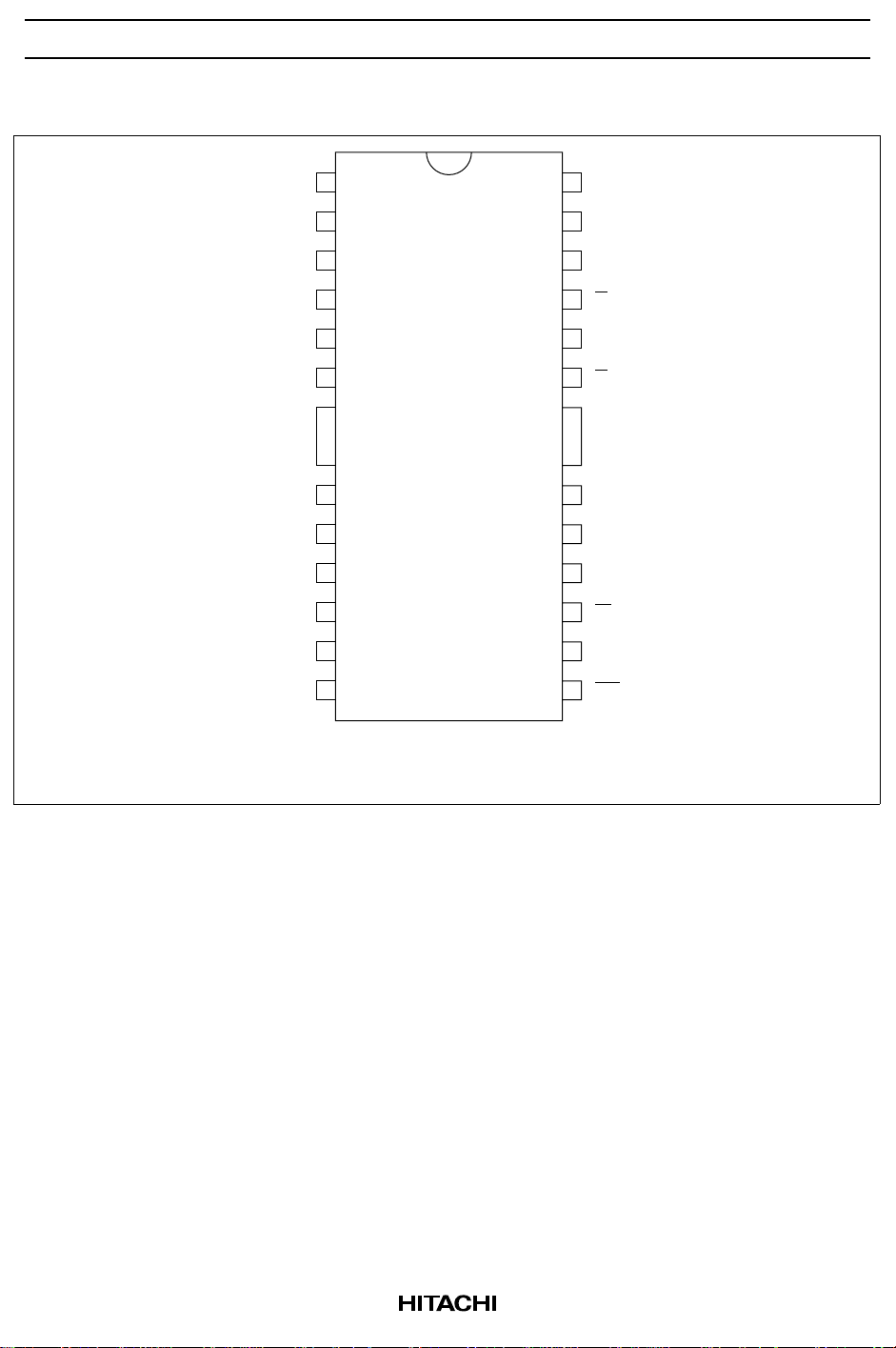
Pin Arrangement
INSEL
CK2/DIR
CK1
Rt
NC
Ct
GND
V0
NC
V1
V2
DAOUT
VREG
1
2
3
4
5
6
TAB
7
8
9
10
11
12
24
23
22
21
20
19
TAB
18
17
16
15
14
13
EXSEL
V
CC
U
U
NC
V
GND
V
NC
W
W
SENSE
OE
(Top view)
2
Page 3
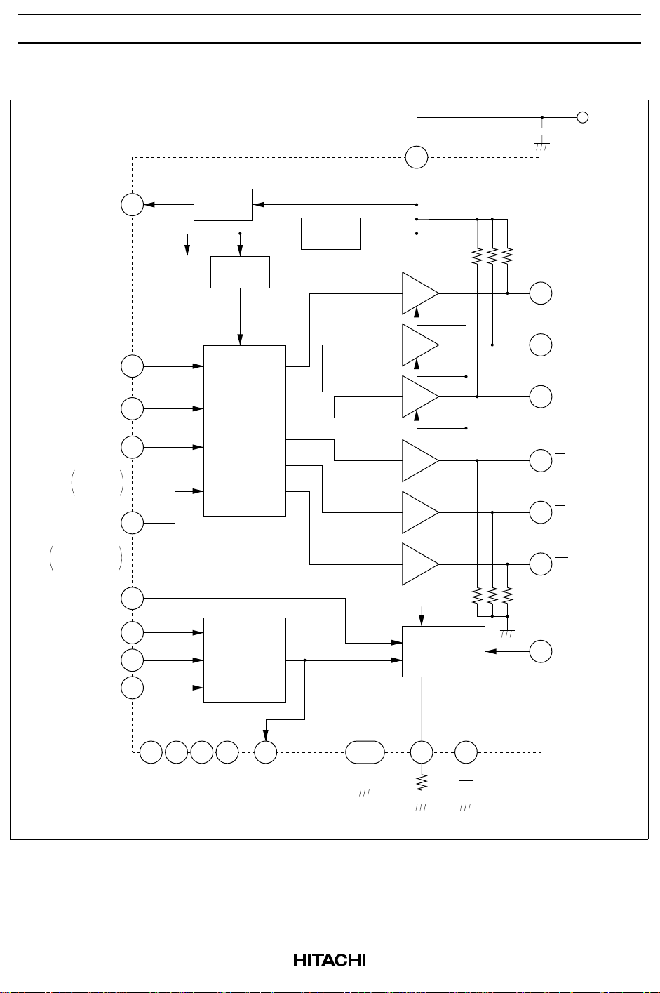
Block Diagram
23
HA13532NT
V
CC
C101
INSEL
H:L:CK2
DIR
Excite select
EXSEL
2ø
H:
2 — 3ø
L:
12VREG REG
LVI
3CK1
2CK2/DIR
Commutation
1Input select
24
13OE
10V2
9V1
7V0
POR
logic
3 bit
DAC
LVI
LVI
PWM
control
Ru
22 U
18 V
16 W
21 U
19 V
15 W
Rd
14 SENSE
LVI:
Low-voltage inhibit circuit
POR:
Power-on reset circuit
5 8 17 20 11
DAOUT
TAB 4 6
Rt Ct
3
Page 4

HA13532NT
Pin Description
Pin No. Pin Name Function Pin Voltage
1 INSEL Selects pin 2 input: CK2 if high; DIR if low (see
timing diagrams)
2 CK2/DIR CK2 or DIR input (see timing diagrams) VTH = 2.5 V typ
3 CK1 CK1 input (see timing diagrams) VTH = 2.5 V typ
4 Rt Reference value for 3-phase output current
and Ct charge/discharge current
5 NC No connection
6 Ct Time constant for PWM carrier frequency
7 V0 Voltage programming input to DAC (LSB) VTH = 2.5 V typ
8 NC No connection
9 V1 Voltage programming input to DAC VTH = 2.5 V typ
10 V2 Voltage programming input to DAC (MSB) VTH = 2.5 V typ
11 DAOUT DAC output
12 VREG Regulated output 4.8 V typ (@I = 2 mA)
13 OE Output enable: low enables PWM output
phases U, V, and W; high gives high
impedance
14 SENSE Current feedback 0 V min, 5.0 V max
15 W Phase-W lower-arm output
16 W Phase-W upper-arm output
17 NC No connection
18 V Phase-V upper-arm output
19 V Phase-U lower-arm output
20 NC No connection
21 U Phase-U lower-arm output
22 U Phase-U upper-arm output
23 V
24 EXSEL Selects exciting mode: 2-phase if high; 2-3-
CC
Power supply 10 V min, 27.6 V max
phase if low (see timing diagrams)
= 2.5 V typ
V
TH
4.8 V typ
VTH = 2.5 V typ
VTH = 2.5 V typ
4
Page 5
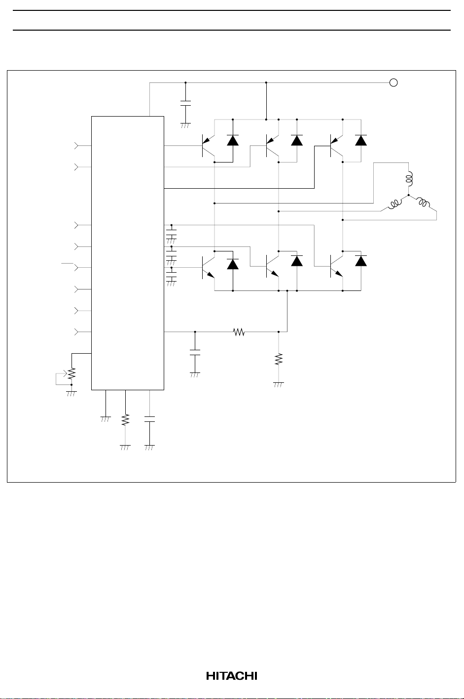
Application Circuit
CK1
3
23
22
C101
Q1
D1
Q2
D2
Q3
HA13532NT
V
CC
D3
CK2/DIR
INSEL
EXSEL
VR101
OE
V2
V1
V0
2
1
24
13
10
9
7
11
TAB 4 6
18
16
15
19
21
14
C102
C103
Q4
C104
C105
CtRt
D4
R101
Q5
D5
Rnf
Q6
D6 *1
Notes: 1. Use high-speed diodes for D4, D5, and D6.
5
Page 6

HA13532NT
External Conponents
Symbol Recommended Value Purpose Notes
Rnf 0.11 Ω ≤ Rnf ≤ 0.33 Ω Current sensing 1
Rt 51 k Ω Reference current programming 2
Ct 1000 pF Time constant for PWM carrier frequency 3
C
101
C
, C
, C
102
103
104
C
105
R
101
VR
101
Notes: 1. The maximum motor drive current is:
Imax ±≈
where, Vdac: DAC output voltage (see electrical characteristics)
2. The output sink current Iosnk, output source current Iosrc, and Ct charge/discharge currents Ict+
and Ict– are calculated as follows:
where, set Rt to be 2.5kΩ or higher.
Iosnk –≈
≥ 0.1 µF Power supply decoupling
0.01 µF Penetration current control 4
1000 pF Current sensing filter
750 Ω
100 kΩ Motor current little adjustment
Vdac + Voffs
Rnf
(1)
Voffs: Offset voltage (see electrical characteristics)
50Vrt
Rt
Vbe
Ru
(2)
Iosrc –≈
50Vrt
Ict+, Ict– ≈
Rt
Vrt
Rt
Vbe
Rd
(3)
(4)
where, Vrt: Rt voltage (see electrical characteristics)
Ru: pull-up resistance (see electrical characteristics)
Rd: pull-down resistance (see electrical characteristics)
Vbe: base-emitter voltage of driven transistor
3. The PWM carrier frequency fc is calculated as follows:
fc ≈
≈
Ict
2Ct (Vcth – Vctl)
Vrt
2CtRt (Vcth – Vctl)
(5)
(6)
where, Vcth: Ct high voltage (see electrical characteristics)
Vctl: Ct low voltage (see electrical characteristics)
4. Values of C
102
, C
103
, C
104
, C
, R
are different from using power transistor
105
101
6
Page 7

Timing Waveforms
Two Clock Pulse Inputs, Two-Phase Exciting (INSEL High, EXSEL High)
HA13532NT
Clock pulse input
CK1
CK2
Output current
*
U
V
W
U
V
W
H
L
H
L
+
0
+
0
+
0
0
–
0
–
0
–
123456789101112 11109876
0
Note: Initialized with U and V on at power-up.*
Two Clock Pulse Inputs, Two-Three-Phase Exciting (INSEL High, EXSEL Low)
Clock pulse input
CK1
H
L
123456789101112 11109876
0
CK2
Output current
U
V
W
U
V
W
Note: Initialized with U and V on at power-up.*
H
L
*
+
0
+
0
+
0
0
–
0
–
0
–
7
Page 8

HA13532NT
One Clock Pulse Input, Two-Three-Phase Exciting (INSEL Low, EXSEL Low)
Clock pulse input
CK1
DIR
Output current
U
V
W
U
V
W
H
L
H
L
*
+
0
+
0
+
0
0
–
0
–
0
–
123456789101112 111098760
Note: Initialized with U and V on at power-up.*
One Clock Pulse Input, Two-Phase Exciting (INSEL Low, EXSEL High)
Clock pulse input
CK1
H
L
123456789101112 11109876
0
H
DIR
L
Output current
Note: Initialized with U and V on at power-up.
*
+
U
0
+
V
0
+
W
0
0
U
–
0
V
–
0
W
–
*
8
Page 9

PWM Control
HA13532NT
Vcth
Ct
Vctl
1/fc
Imax
Im
Vdac
Rnf
0
Iosnk
Output current
*
0
Note: * Only phase U is shown.
Absolute Maximum Ratings
Item Symbol Rating Unit Notes
Power supply voltage V
Input voltage Vin 7 V 2
Power dissipation P
Operating temperature Topr –10 to +70 °C
Storage temperature Tstg –55 to +125 °C
Output current Ireg 2 mA
Notes: 1. The operating power supply voltage range is VCC = 10 V to 27.6 V.
2. Applies to logic and DAC input pins.
3. Permitted at Ta = 70°C, if thermal resistance is as below:
θj – a ≤ 60°C/W (glass-epoxy board)
CC
T
30 V 1
910 mW 3
9
Page 10

HA13532NT
Electrical Characteristics (Ta = 25°C, VCC = 24 V)
Item Symbol Min Typ Max Unit
Current
consumption
REG Output
voltage
Load
regulation
Logic Input cur-
rent
Low voltage
level
High
voltage
level
DAC Outout volt-
age
PWM control Input
current
Offset volt-
age
Rt voltage Vrt 4.4 4.8 5.2 V Rt = 51 kΩ 4
Ct change
current
Ct
discharge
current
I
CCO
I
CC
Vreg 4.4 4.8 5.2 V Ireg = 2 mA 12
∆Vreg — — ±0.1 V Ireg = 0 mA to
lin –10 — 1 µA Vin = 0 V to 7V1, 2, 3,
Vil — — 1.35 V 1, 2, 3,
Vih 3.65 — — V 24
Vdac 200 230 260 mV (V2, V1, V0)
Isens — — ±2 µA Vsens = 0 V to
Voffs — — ±10 mV 2
Ict+ 84 94 104 µA Rt = 51 kΩ, Vct
Ict– 84 94 104 µA Rt = 51 kΩ, Vct
— — 33 mA VCC = 30 V, OE
— — 41 mA VCC = 30 V, OE
–1 — 10 µA 7, 9, 10
116 146 176 mV (V2, V1, V0)
75 105 135 mV (V2, V1, V0)
33 63 93 mV (V2, V1, V0)
Test
Conditions Pins Notes
23 1
= H
= L
2 mA
13, 24
7, 9, 10,
13,
11
= (H, L, L)
= (L, H, L)
= (L, L, H)
= (L, L, L)
14
5 V
6
= 3.75 V
= 3.75 V
10
Page 11

Electrical Characteristics (Ta = 25°C, VCC = 24 V) (Cont)
CC
CC
Item Symbol Min Typ Max Unit
PWM control Ct high
voltage
Ct low
voltage
Carrier
frequency
3-pahse
output
Output sink
current
Output
source
current
Output leakage current
Pull-up
resistance
Pull-down
resistance
Transient
response
time
LVI Operating
voltage
Hysteresis Vhys — 0.3 — V
Notes: 1. Measured with pins 12, 15, 16, 18, 19, 21, and 22 open.
2. Offset between pins 11 and 14.
3. See timing diagrams.
Vcth 4.3 4.8 5.3 V 6 3
Vctl 2.3 2.78 3.3 V
fc 18.6 23.3 28.0 kHz Rt = 51 kΩ,
Iosnk 2.0 3.1 4.2 mA VO = VCC – 1.5
Iosrc 2.0 3.1 4.2 mA VO = 1.5 V,
Ioff — — ±10 µAV
——±10 µAV
Ru 700 950 1200 Ω 16, 18,
Rd 700 950 1200 Ω 15, 19,
t
phl
t
plh
— — 6.0 µs 15, 16,
— — 6.0 µs
Vlvi 8.0 — 10 V 23
HA13532NT
Test
Conditions Pins Notes
Ct = 1000 pF
16, 18,
V, Rt = 51 kΩ
Rt = 51 kΩ
= 30 V,
V
= V
O
CC
= 30 V,
V
= 0 V
O
22
15, 19,
21
16, 18,
22
15, 19,
21
22
21
18, 19,
21, 22
11
Page 12

HA13532NT
Reference Data
40
*2
30
CCO
*1
CC
Icc
Icco
20
10
Current consumption I , I (mA)
0
10 15 20 25 30
Supply voltage V (V)
CC
400
(V2, V1, V0) = (H, H, H)
5.2
5.0
Output voltage Vreg (V)
4.8
0.8 1.2 1.6 2.0
0.40
Output current Ireg (mA)
400
(V2, V1, V0) = (H, H, H)
(V2, V1, V0) = (H, H, L)
300
200
DAC Output voltage Vdac (mV)
(V2, V1, V0) = (H, L, H)
(V2, V1, V0) = (H, L, L)
(V2, V1, V0) = (L, H, H)
(V2, V1, V0) = (L, H, L)
(V2, V1, V0) = (L, L, H)
100
(V2, V1, V0) = (L, L, L)
0
0204060
-10 10 30 50 70
300
200
Output voltage Vdac (mV)
100
0
10 15 20 25 30
Ambient temperature Ta (°C)
Notes: 1. Iosnk + Iosrc is the current during three-channel output.
2.Iosnk is the current during two-channel output.
(V2, V1, V0) = (H, H, L)
(V2, V1, V0) = (H, L, H)
(V2, V1, V0) = (H, L, L)
(V2, V1, V0) = (L, H, H)
(V2, V1, V0) = (L, H, L)
(V2, V1, V0) = (L, L, H)
(V2, V1, V0) = (L, L, L)
Supply voltage V (V)
CC
12
Page 13

HA13532NT
3.3
3.2
3.1
3.0
Output sink current Iosnk (mA)
2.9
2.8
-10 10 30 50 70
0204060
Ambient temperature Ta (°C)
3.3
3.2
3.1
3.0
2.9
Output source current Iosrc (mA)
2.8
-10 10 30 50 70
0204060
Ambient temperature Ta (°C)
13
Page 14

HA13532NT
In-Circuit Waweform Characteristics
Ct
(2 V/div)
GND
Rnf
(200 mV/div)
GND
V
CC
Phase-U output
(2 V/div)
t (20 µs/div)
CK1
(2 V/div)
GND
V
CC
Phase-U output
(1 V/div)
t (5 ms/div)
14
Page 15

Package Dimensions
1
HA13532NT
Unit: mm
27.10
28.10 Max
1324
8.8
10.0 Max
12
1.0
10.16
1.778 ± 0.250
4.036 0.48 ± 0.10
0.76
0.51 Min
Hitachi code
JEDEC code
5.08 Max
2.54 Min
0° – 15°
EIAJ code
+ 0.11
0.25
– 0.05
DP-24TS
—
—
15
Page 16

Cautions
1. Hitachi neither warrants nor grants licenses of any rights of Hitachi’s or any third party’s patent,
copyright, trademark, or other intellectual property rights for information contained in this document.
Hitachi bears no responsibility for problems that may arise with third party’s rights, including
intellectual property rights, in connection with use of the information contained in this document.
2. Products and product specifications may be subject to change without notice. Confirm that you have
received the latest product standards or specifications before final design, purchase or use.
3. Hitachi makes every attempt to ensure that its products are of high quality and reliability. However,
contact Hitachi’s sales office before using the product in an application that demands especially high
quality and reliability or where its failure or malfunction may directly threaten human life or cause risk
of bodily injury, such as aerospace, aeronautics, nuclear power, combustion control, transportation,
traffic, safety equipment or medical equipment for life support.
4. Design your application so that the product is used within the ranges guaranteed by Hitachi particularly
for maximum rating, operating supply voltage range, heat radiation characteristics, installation
conditions and other characteristics. Hitachi bears no responsibility for failure or damage when used
beyond the guaranteed ranges. Even within the guaranteed ranges, consider normally foreseeable
failure rates or failure modes in semiconductor devices and employ systemic measures such as failsafes, so that the equipment incorporating Hitachi product does not cause bodily injury, fire or other
consequential damage due to operation of the Hitachi product.
5. This product is not designed to be radiation resistant.
6. No one is permitted to reproduce or duplicate, in any form, the whole or part of this document without
written approval from Hitachi.
7. Contact Hitachi’s sales office for any questions regarding this document or Hitachi semiconductor
products.
Hitachi, Ltd.
Semiconductor & Integrated Circuits.
Nippon Bldg., 2-6-2, Ohte-machi, Chiyoda-ku, Tokyo 100-0004, Japan
Tel: Tokyo (03) 3270-2111 Fax: (03) 3270-5109
URL NorthAmerica : http:semiconductor.hitachi.com/
For further information write to:
Hitachi Semiconductor
(America) Inc.
179 East Tasman Drive,
San Jose,CA 95134
Tel: <1> (408) 433-1990
Fax: <1>(408) 433-0223
Europe : http://www.hitachi-eu.com/hel/ecg
Asia (Singapore) : http://www.has.hitachi.com.sg/grp3/sicd/index.htm
Asia (Taiwan) : http://www.hitachi.com.tw/E/Product/SICD_Frame.htm
Asia (HongKong) : http://www.hitachi.com.hk/eng/bo/grp3/index.htm
Japan : http://www.hitachi.co.jp/Sicd/indx.htm
Hitachi Europe GmbH
Electronic components Group
Dornacher Stra§e 3
D-85622 Feldkirchen, Munich
Germany
Tel: <49> (89) 9 9180-0
Fax: <49> (89) 9 29 30 00
Hitachi Europe Ltd.
Electronic Components Group.
Whitebrook Park
Lower Cookham Road
Maidenhead
Berkshire SL6 8YA, United Kingdom
Tel: <44> (1628) 585000
Fax: <44> (1628) 778322
Hitachi Asia Pte. Ltd.
16 Collyer Quay #20-00
Hitachi Tower
Singapore 049318
Tel: 535-2100
Fax: 535-1533
Hitachi Asia Ltd.
Taipei Branch Office
3F, Hung Kuo Building. No.167,
Tun-Hwa North Road, Taipei (105)
Tel: <886> (2) 2718-3666
Fax: <886> (2) 2718-8180
Copyright ' Hitachi, Ltd., 1999. All rights reserved. Printed in Japan.
Hitachi Asia (Hong Kong) Ltd.
Group III (Electronic Components)
7/F., North Tower, World Finance Centre,
Harbour City, Canton Road, Tsim Sha Tsui,
Kowloon, Hong Kong
Tel: <852> (2) 735 9218
Fax: <852> (2) 730 0281
Telex: 40815 HITEC HX
 Loading...