

Page 1
Global Mixed-mode Technology Inc.
Fan Speed PWM Controller
Features
Constant Fan Speed Control
PWM control for stable operation
Build-in MOSFET switch
SMBus interface
Internal short-circuit protection
On/Off control provided
Applications
Notebook PC
Industrial PC
LAN Switch
Servers
Telecom equipment
Industrial Control
G760A
General Description
G760 is a single chip solution for fan speed control,
packaged in a space saving SO-8 package. It connects directly to the fan and performs closed-loop
control of the fan speed. The only external component required is a 10µF capacitor. It determined the
current fan speed based on the fan rotation pulses
and an externally supplied clock. It uses pulse width
modulation (PWM) method and an on-chip
MOSFET to control the fan speed to ±2% of the
programmed speed. The desired fan speed is programmed via the SMBus. The actual fan speed and
fan status can be read via the SMBus. Short-circuit
protection is implemented to prevent damages to
the fan and this IC itself. An On/Off control pin is
also provided.
Ordering Information
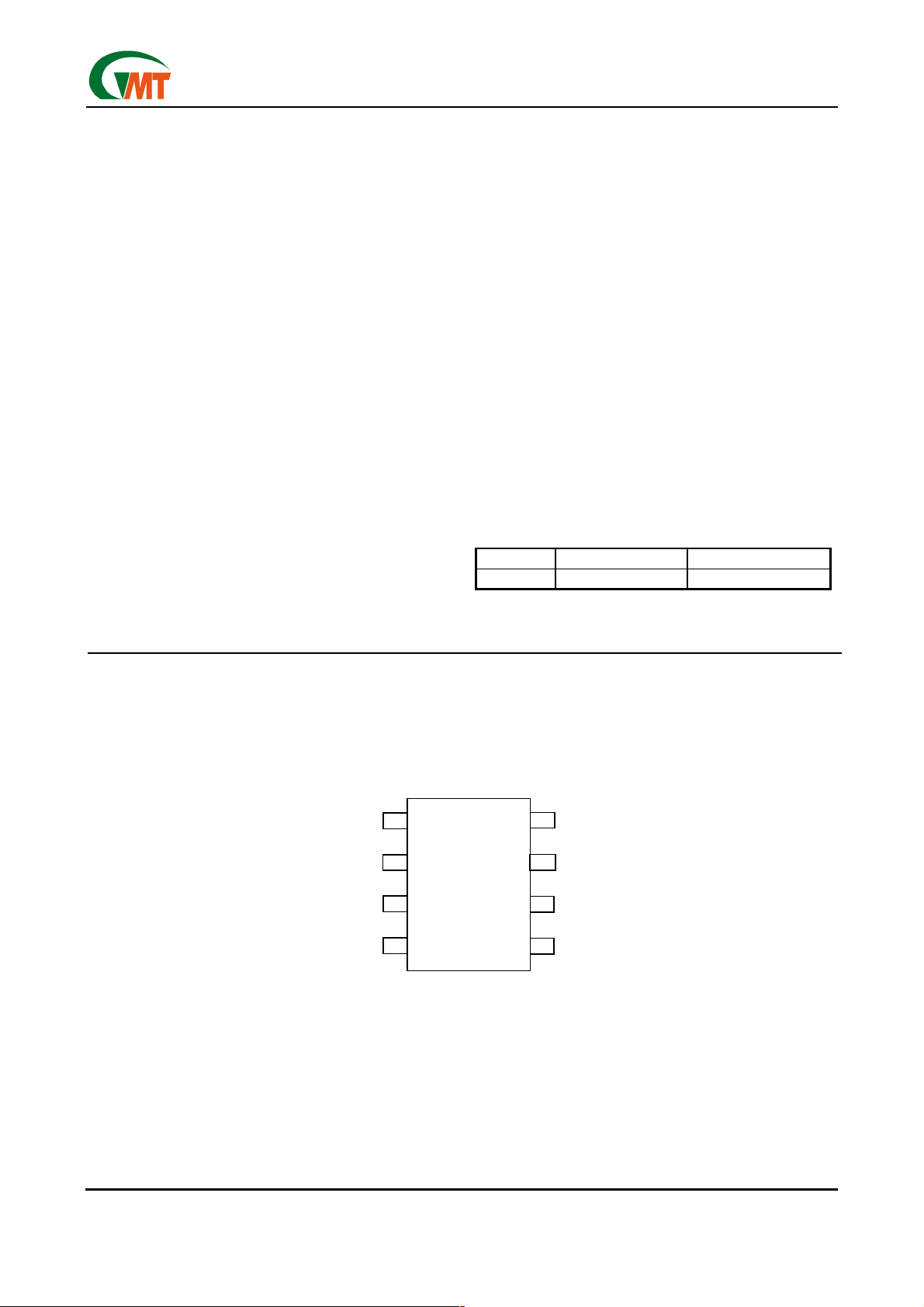
Pin configuration
OUT
OUT
F.G.
F.G.
ON/OFF
ON/OFF
GND
GND
1
1
2
2
3
3
4
4
PART* TEMP. RANGE PIN-PACKAGE
G760A 0°C to +70°C 8-SOP
G760A
G760A
8Pin SOP
8Pin SOP
V
V
8
8
7
7
SMBDATA
SMBDATA
6
6
SMBCLKLK
SMBCLKLK
5
5
CLK
CLK
CC
CC
Ver 4.3
Oct 28, 2002
1
TEL: 886-3-5788833
http://www.gmt.com.tw
Page 2
Global Mixed-mode Technology Inc.
G760A
Absolute Maximum Ratings
PARAMETER SYMBOL MAXIMUM UNITS
Supply Voltage VCC -0.3 to +7 V
Operating Temperature Range TA 0 to +70 °C
Junction Temperature Range TJ 0 to +125 °C
Storage Temperature Range T
-65 to +150 °C
STG
Lead Temperature (solding) 10 seconds TL 300 °C
Electrical Characteristics
(Unless specified: VCC = 5V, TA = 25°C)
PARAMETER CONDITIONS MIN TYP MAX UNITS
Supply voltage VCC 4.5 5 5.5 V
Shutdown current On/Off = 0V 2 5 µA
MOSFET on resistance 0.2 0.25
Short-circuit current limit 0.5 A
Input logic low VIL 0.8 V
Input logic high VIH 2.4 V
Average Output current 350 mA
FG input Positive-going threshold voltage VCC=5V 1.8 V
FG input Negative-going threshold voltage VCC=5V 0.7 V
FG input Hysteresis voltage VCC=5V 1.1 V
Ω
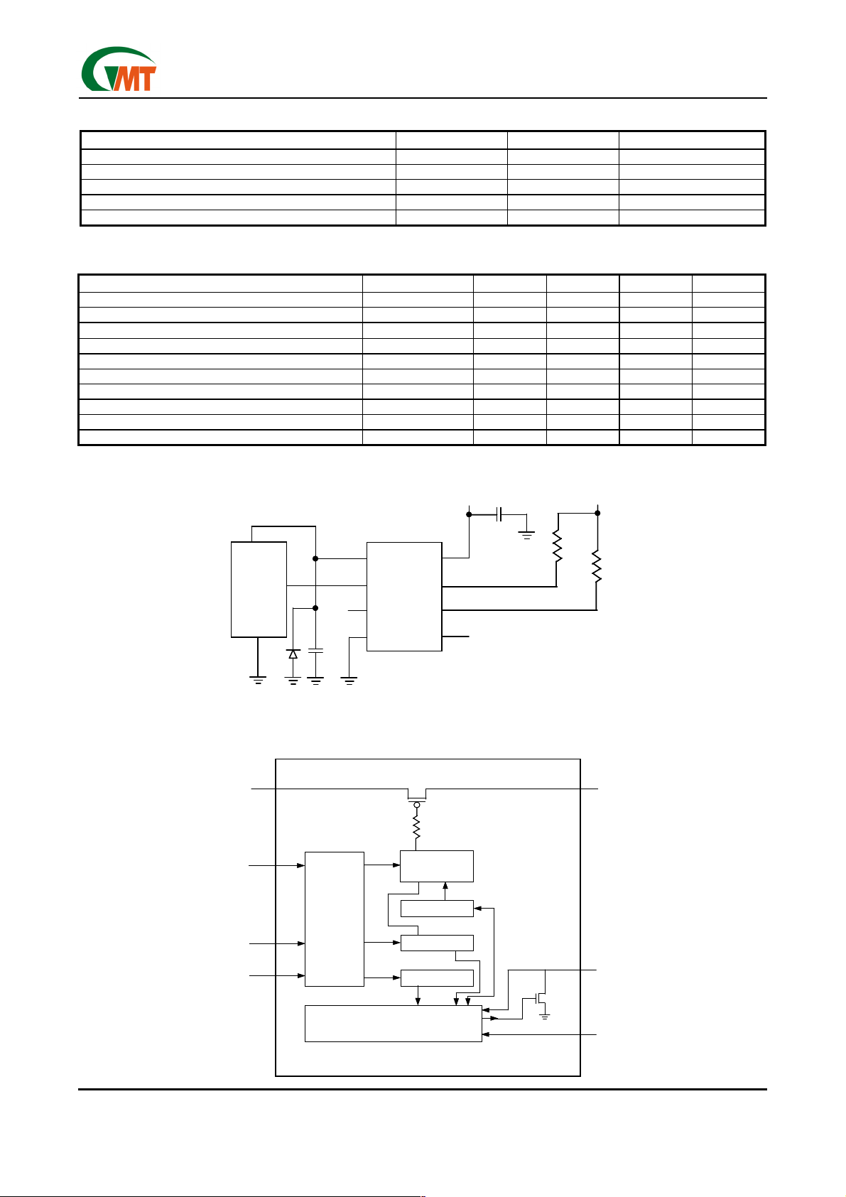
Application Circuit
3.3V to 5V
5V
5V
10µF
10µF
3.3V to 5V
Diode 1N4148 is optional
Block Diagram
OUT
OUT
ON/OFF
ON/OFF
10k
V
V
IN
IN
FG
FG
FAN
FAN
*
*
1N4148
1N4148
FG
FG
ON/OFF
ON/OFF
10 µF
10 µF
FAN
FAN
CONTROL
CONTROL
LOGIC
LOGIC
1
1
2
2
3
3
4
4
8
8
7
7
6
6
5
5
PWM DUT Y
PWM DUT Y
LOGIC
LOGIC
SET_CNT
SET_CNT
ACT_CNT
ACT_CNT
32.768KHz
32.768KHz
10k
10k
10k
VCC
VCC
Ver 4.3
Oct 28, 2002
CLK
CLK
SMBus CONTROL
SMBus CONTROL
LOGIC
LOGIC
FAN_STA
FAN_STA
2
SMBDATA
SMBDATA
SMBCLK
SMBCLK
TEL: 886-3-5788833
http://www.gmt.com.tw
Page 3

Global Mixed-mode Technology Inc.
Pin Description
PIN NO. PIN NAME PIN FUNCTION
1 OUT PWM output, connect to fan
2 F.G. FAN pulse Input
3 ON/OFF ON/OFF control pin, 0V means shutdown
4 GND Ground
5 CLK Clock input for fan speed measurement
6 SMBCLK SMBus clock line
7 SMBDATA SMBus data line
8 VCC Supply voltage
Description
The fan speed is measured by counting the number of
the CLK pin period between the rising edges of two
fan speed pulses on FG pin. In this way, we are actually measuring the period of the fan speed. To avoid
the cost of doing division to obtain the speed, this
count number, N, is used in the PWM control algorithm, thus, the desired fan speed should be programmed by writing the corresponding count number.
The count number is given by:
N = (CLK x 30) / (rpm x P)
N : Count Number
P : FG pulses number per revolution of fan.
For CLK = 32768Hz, P = 2
⇒
N = 491520 / rpm
For CLK = 16384Hz, P = 2
⇒
N = 245762 / rpm
Some selected count numbers are shown below
Table 1. Count numbers for P=2
rpm CLK=32768Hz CLK=16384Hz
968 --- 254
1935 254 127
2000 246 123
3000 164 82
4000 123 61
5000 98 49
6000 82 41
7000 70 35
8000 61 31
9000 55 27
10000 49 25
20000 25 12
30000 16 8
When pin 3 (On/Off) is a logical 1, the fan speed will
be controlled according to the setting in the programmed fan speed register. There are two ways to
stop the fan, (1)setting pin 3 (On/Off) to 0V, (2) program the fan speed register to 255. These also makes
the fan controller into power saving mode.
Controlling Fan at Lower Speed
For stably controlling fans at lower rotation speed,
three schemes are recommended as below:
1.Use larger decoupling capacitors between FAN_OUT
and GND.
2.Shunt a capacitor of 1µF-2µF on FG pin to GND.
3.Use fans with open-collector FG outputs.
When controlling fans under lower rotation speed, the
output voltage of FAN_OUT would be too low for fan
to generate recognizable FG signals.
Using decouple capacitors on FAN_OUT and FG is to
increase the SNR on FG pins. While using fans with
open_collector FG outputs can thoroughly solve the
problem, because the logic high level of FG would be
fixed to 5V.
G760A
Ver 4.3
Oct 28, 2002
3
TEL: 886-3-5788833
http://www.gmt.com.tw
Page 4

Global Mixed-mode Technology Inc.
Internal Registers
This IC provides 3 SMBus registers.
1.Programmed fan speed register:(SET_CNT,address:00b)
This register is a read/write register, it contains the
count number of the desired fan speed. Power up
default is FFh.
2.Actual fan speed register: (ACT_CNT, address: 01b)
the actual fan speed. Power up default is FFh.
3.Fan status register: (FAN_STA , address : 10b)
This register is read only. Its bit 0 is set to 1 when
the actual fan speed is ±20% outside the desired
speed. Its bit 1 is set to 1 when fan speed is below
1920 rpm. Power up default is 10b.
G760A
This register is read only. It contains the count number of
SMBus Address
The SMBus address of this chip is fixed to7Ch (01111100b) for write and 7Dh(01111101b) for read.
SMBus Timing
1
SMBCLK
SMBCLK
SMBDATA
SMBDATA
Start
Start
by
by
Master
Master
1
91
91
0
1
1
1
0
0
1
1
1
Address Byte
Address Byte
11
11
0
0
R/W
R/W
Ack
Ack
by
by
G760
G760
1
1
1
91
91
91
Pointer Byte
Pointer Byte
0
00000
00000
9
9
D0D1
D0D1
Ack
Ack
by
by
G760
G760
9
9
9
SMBCLK
SMBCLK
SMBDATA
SMBDATA
Start
Start
by
by
Master
Master
1
1
0
0
SMBCLK
SMBCLK
SMBDATA
SMBDATA
111
111
Address Byte
Address Byte
0
0
11
11
11
0
R/W
R/W
R/W
Ack
Ack
Ack
by
by
by
G760
G760
G760
Data Byte
Data Byte
Data Byte
Repeat
Repeat
Repeat
Start
Start
Start
by
by
by
Master
Master
Master
0
0
0
1
1
1
1
1
1
1
1
1
Address Byte
Address Byte
Address Byte
(a) Typical Pointer Set Followed by Immediate Read
1
1
91
91
D7
Start
Start
by
by
Master
Master
0
0
1
1
1
1
1
1
Address Byte
Address Byte
110
110
R/W
R/W
Ack
Ack
by
by
G760
G760
D7
(b) Typical 1-Byte Read with Preset Pointer
1
1
9
9
0
11
11
0
0
R/W
R/W
Ack
Ack
by
by
G760
G760
00000
00000
Pointer Byte
Pointer Byte
0
D0D1
D0D1
Ack
Ack
G760
G760
0
0
111
111
Address Byte
by
by
Address ByteAddress Byte
(a) Typical Pointer Set Followed by Immediate Read
D3D4D5D6D7
D3D4D5D6D7
D3D4D5D6D7
Data Byte
Data Byte
11
11
D0D1D2
D0D1D2
D0D1D2
No Ack
No Ack
No Ack
Master
Master
Master
D0
D1D2
D0
D1D2
D3D4D5D6
D3D4D5D6
919
919
D6
D6
D7
D7
R/W
R/W
0
0
Ack
Ack
by
by
G760
G760
by
by
by
D5
D5
Master
Master
Master
9
9
No Ack
No Ack
by
by
Master
Master
Data Byte
Data ByteData Byte
Stop
Stop
Stop
Cond
Cond
Cond
by
by
by
Master
Master
D3D4
D3D4
Stop
Stop
Cond
Cond
by
by
9
9
D0
D1D2
D0
D1D2
Stop
Stop
No Ack
No Ack
Cond
Cond
by
by
by
by
Master
Master
Master
Master
SMBCLK
SMBCLK
SMBDATA
SMBDATA
Ver 4.3
Oct 28, 2002
Start
Start
by
by
Master
Master
1
1
91
91
0
0
000
1
0
0
1
1
1
1
Address Byte
Address Byte
1
1
1
1
1
0 D0
0 D0
R/W
R/W
Ack
Ack
by
by
G760
G760
000
0
0
Pointer Byte
Pointer Byte
0
0
D1
D1
Ack
Ack
by
by
Master
Master
D7
D7
D5D6
D5D6
Configuration Byte
Configuration ByteConfiguration Byte
D2D3D4
D2D3D4
919
919
D1
D1
D0
D0
Stop
Stop
Ack
Ack
Cond
Cond
by
by
by
by
G760
G760
Master
Master
(b) Register Write
TEL: 886-3-5788833
http://www.gmt.com.tw
4
Page 5

Global Mixed-mode Technology Inc.
Package Information
(4X)
°
7
y
B
G760A
C
E
H
L
D
θ
A2
A
e
A1
Note:
1. Package body sizes exclude mold flash and gate burrs
2. Dimension L is measured in gage plane
3. Tolerance 0.10mm unless otherwise specified
Controlling dimension is millimeter converted inch dimensions are not necessarily exact.
4.
SYMBOL
A 1.35 1.60 1.75 0.053 0.063 0.069
A1 0.10 ----- 0.25 0.004 ----- 0.010
A2 ----- 1.45 ----- ----- 0.057 -----
B 0.33 ----- 0.51 0.013 ----- 0.020
C 0.19 ----- 0.25 0.007 ----- 0.010
D 4.80 ----- 5.00 0.189 ----- 0.197
E 3.80 ----- 4.00 0.150 ----- 0.157
e ----- 1.27 ----- ----- 0.050 -----
H 5.80 ----- 6.20 0.228 ----- 0.244
L 0.40 ----- 1.27 0.016 ----- 0.050
y ----- ----- 0.10 ----- ----- 0.004
θ
MIN. NOM. MAX. MIN. NOM. MAX.
0º ----- 8º 0º ----- 8º
DIMENSION IN MM DIMENSION IN INCH
Taping Specification
Feed Direction
Feed Direction
Typical SOP Package Orientation
Typical SOP Package Orientation
GMT Inc. d oes not assume any responsibility for use of any circuitry described, no circuit patent li censes are implied and GMT Inc. reserves the right at any time without notice to change said circuitry and specifications.
Ver 4.3
Oct 28, 2002
5
TEL: 886-3-5788833
http://www.gmt.com.tw
 Loading...