

Page 1
Global Mixed-mode Technology Inc.
G751
Digital Temperature Sensor and Thermal Watchdog
with Two-Wire Interface
General Description
Features
SMBus interface
Programmable Trip Point (TOS) and Hysteresis
(T
)
HYST
Separate open-drain output pin operates as
interrupt or comparator at output
Register readback capability
Power up defaults permit stand-alone opera-
tion as thermostat
Shutdown mode to minimize power consump-
tion
Up to 8 G751s can be connected to a single
bus
Key Specifications
Supply Voltage 3.0V to 5.5V
Supply Current operating 280µA (typ)
1mA (max)
shutdown 2µA(typ)
Temperature Accuracy
-25°C to 100°C ±2°C (max)
-55°C to 125°C ±3°C (max)
Applications
System Thermal Management
Personal Computers
Office Electronics
Electronic Test Equipment
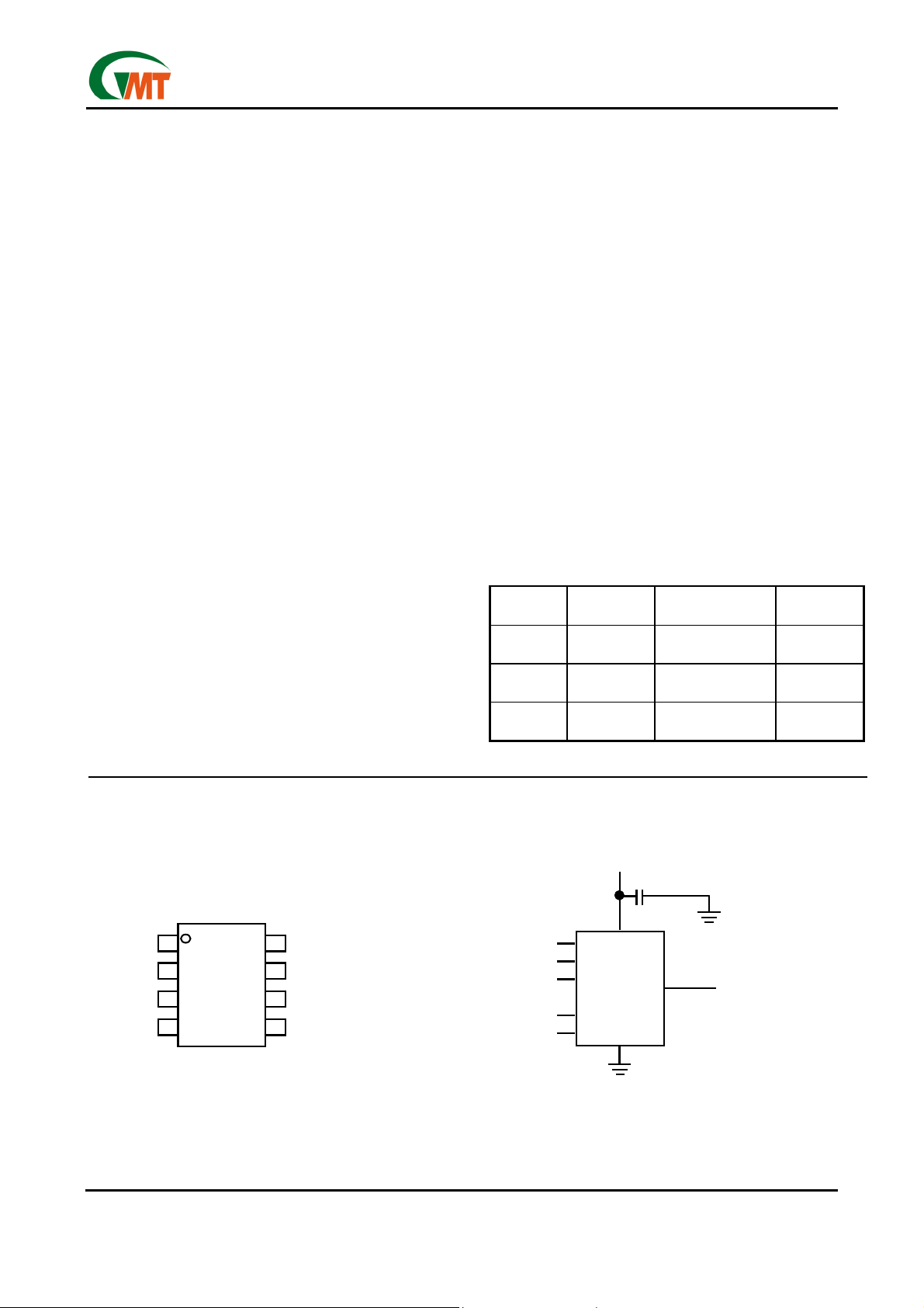
Pin Configuration
The G751 is a temperature sensor, Delta-Sigma
analog-to-digital converter, and digital over- temperature detector with SMBus
interface. The host
can query the G751 at any time to read temperature.
The open-drain Over temperature Shutdown (O.S.)
output becomes active when the temperature exceeds a programmable limit. This pin can operate in
either “Comparator” or “Interrupt” mode.
The host can program both the temperature alarm
threshold (T
alarm condition goes away (T
host can read back the contents of the G751’s T
and T
HYST
parator mode with default thresholds of 50°C T
45°C T
HYST.
) and the temperature at which the
OS
). In addition, the
HYST
OS
registers. The sensor powers up in Com-
OS
for G751-1 and 80°C T
, 75°C T
OS
HYST
for G751-2.
Ordering Information
PART T
G751-1P1 50°C/45°C
G751-2P1 80°C /75°C
G751-2P8 80°C /75°C
OS THYST
TRANSPORT
MEDIA
2500 Units on Tape
and Reel
2500 Units on Tape
and Reel
2500 Units on Tape
and Reel
PACKAGE
8 SOP
8 SOP
8 MSOP
P1: 8 SOP; P8: 8 MSOP
Typical Application
SMBDATA
SMBDATA
SMBCLK
SMBCLK
O.S.
O.S.
GND
GND
Ver: 2.4
Nov 26, 2002
G751
G751
1
1
2
2
3
3
45
45
8Pin SOP/MSOP
8Pin SOP/MSOP
8
+Vs
8
+Vs
A0
A0
7
7
6
6
A1
A1
A2
A2
Address(Set as
Address(Set as
Address(Set as
desired)
desired)
desired)
Interface
Interface
Interface
1
A0
A0
A0
A1
A1
A1
A2
A2
A2
SMBDATA
SMBDATA
SMBDATA
SMBCLK
SMBCLK
SMBCLK
+VS 3V to 5.5V
+VS 3V to 5.5V
+VS 3V to 5.5V
7
7
7
6
6
6
5
5
5
1
1
1
2
2
2
8
8
8
3
3
G751
G751
G751
4
4
4
3
O.S. Out
O.S. Out
O.S. Out
O.S. Set for active low for
O.S. Set for active low for
O.S. Set for active low for
wire OR’d multiple
wire OR’d multiple
wire OR’d multiple
interrupt line
interrupt line
interrupt line
Typical Bypass 0.1 µF
Typical Bypass 0.1 µF
Typical Bypass 0.1 µF
(Unless mounted close
(Unless mounted close
(Unless mounted close
to Processor)
to Processor)
to Processor)
To Processor
To Processor
To Processor
Interrupt Line
Interrupt Line
Interrupt Line
TEL: 886-3-5788833
http://www.gmt.com.tw
Page 2
Global Mixed-mode Technology Inc.
G751
Absolute Maximum Ratings.
Supply Voltage………….…………………-0.3V to 6.5V
Voltage at any Pin……………….…-0.3V to +Vs +0.3V
Input Current at any Pin…………………………….5mA
Operating Ratings
Specified Temperature Range…………….T
-55°C to +125°C
Supply Voltage Range (+Vs)…………..+3.0V to +5.5V
MIN
to T
MAX
Package Input Current…………………………….20mA
O.S. Output Sink Current………………………….10mA
O.S. Output Voltage…………………….…………..6.5V
Storage Temperature…………………-65°C to +150°C
Soldering Information, Lead Temperature
SOP Package
Vapor Phase (60 seconds)……………………….215°C
Infrared (15 seconds)……………………………..220°C
ESD Susceptibility
Human Body Model……………………………….2000V
Machine Model……………………………………...200V
Temperature-to-Digital Converter Characteristics
Unless otherwise noted, these specifications apply for +Vs=+3.3v Vdc.
; all other limits TA=TJ= +25°C, unless otherwise noted.
T
MAX
PARAMETER CONDITIONS TYPICAL LIMITS UNITS
Accuracy
Resolution 9
Temperature Conversion Time 100
Quiescent Current
O.S. Output Saturation Voltage I
O.S. Delay
TOS Default Temperature G751-1/G751-2 50/80 °C
T
Default Temperature G751-1/G751-2 45/75 °C
HYST
TA=-25°C to +100°C
TA=-55°C to +125°C
SMBus Inactive
SMBus Active
Shutdown Mode
= 4.0mA
OUT
Boldface limits apply for T
±
±
1.0
0.8
2.0
3.0
1
6
Conversions (min)
Conversions (max)
25
0.
1
A=TJ=TMIN
°C (max)
Bits
Ms
Ma
mA (max)
µA
V (max)
to
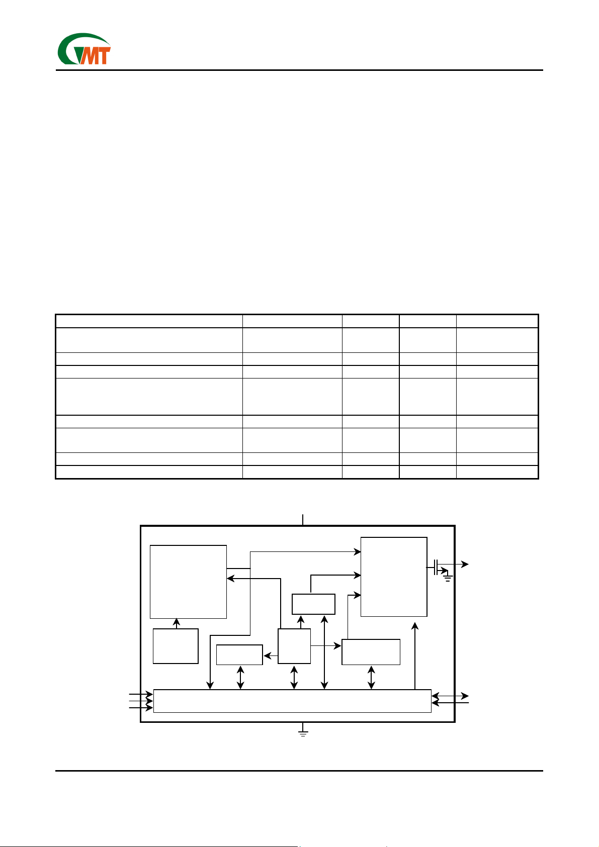
Block Diagram
Ver: 2.4
Nov 26, 2002
+VS3.0V - 5.5V
+VS3.0V - 5.5V
8
8
Temperat ure
Temperat ure
3
3
O.S.
Threshold
T
T
HYST
HYST
Register
Register
Threshold
Set Point
Set Point
Set Point
Set Point
Comparator
Comparator
Reset
Reset
9-Bit Delta-Sigma
9-Bit Delta-Sigma
Analog-to-Digital
Analog-to-Digital
Converter
Converter
Silicon
Silicon
Bandgap
Bandgap
Temperat ure
Temperat ure
Sensor
Sensor
7
7
A0
A0
6
6
A1
A1
5
5
A2
A2
Configuration
Configuration
Register
Register
Two-Wire Interface
Two-Wire Interface
T
T
Pointer
Pointer
Register
Register
Set Point
Set Point
OS
OS
Register
Register
4
4
O.S.
1
1
SMBDATA
SMBDATA
SMBCLK
SMBCLK
2
2
TEL: 886-3-5788833
http://www.gmt.com.tw
2
Page 3
Global Mixed-mode Technology Inc.
G751
Logic Electrical Characteristics
Digital DC Characteristics
Unless otherwise noted, these specifications apply for +Vs=+3.3 Vdc.
; all other limits TA=TJ=+25°C, unless otherwise noted.
T
MAX
SYMBOL PARAMETER CONDITIONS TYPICAL LIMITS UNITS
V
Logical “1” Input Voltage
IN (1)
V
Logical “0” Input Voltage
IN (0)
I
Logical “1”Intput Current VIN=5V 0.005
IN (1)
I
Logical “0”Intput Current VIN=0V -0.005
IN (0)
CIN All Digital Inputs 20
IOH High Level Output Current VOH=5V
VOL Low Level Output Voltage IOL=3ma
tOF Output Fall Time CL=400pF,IO=3ma
SMBus Digital Switching Characteristics
Unless otherwise noted, these specifications apply for +Vs = +3.3 Vdc and C
80pF unless otherwise specified.
Boldface limits apply for T
= TJ = T
A
unless otherwise noted.
The switching characteristics of the G751 fully meet or exceed the published specifications of the SMBus. The
following parameters are the timing relationships between SMBCLK and SMBDATA signals related to the G751.
They are not the SMBus specifications.
Boldface limits apply for T
××××
+Vs
0.7
+Vs + 0.5
-0.3
××××
+Vs
0.3
1.0
-1.0
100
0.4
250
(load capacitance) on output lines =
L
MIN
to T
; all other limits TA = TJ = +25°C,
MAX
A=TJ=TMIN
V (min)
V (max)
V (min)
V (max)
µA
µA
PF
µA (max)
V (max)
ns (max)
to
SYMBOL PARAMETER CONDITIONS TYPICAL LIMITS UNITS
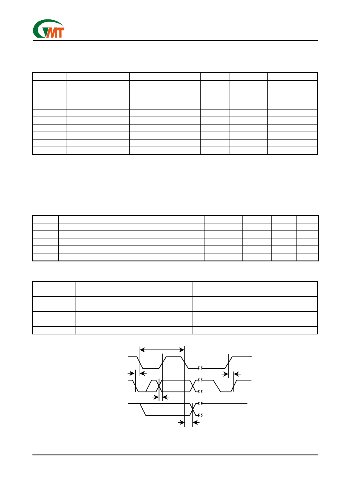
t1 SMBCLK (Clock) Period 2.5 µs (min)
t2 Data in Set-Up Time to SMBCLK High 100 ns (min)
t3 Data Out Stable after SMBCLK Low 0 ns (min)
t4 SMBDATA Low Set-Up Time to SMBCLK Low (Start Condition) 100 ns (min)
t5 SMBDATA High Hold Time after SMBCLK High (Stop Condition) 100 ns (min)
Pin Description
PIN LABEL FUNCTION TYPICAL CONNECTION
1 SMBDATA SMBus Serial Bi-Directional Data Line From Controller
2 SMBCLK SMBus Clock Input From Controller
3 O.S. Overtemperature Shutdown Open Drain Output Pull Up Resistor, Controller Interrupt Line
4 GND Power Supply Ground Ground
5,6,7 A0-A2 User-Set SMBus Address Inputs Ground (Low, “0”) or +Vs (High, “1”)
8 +Vs Positive Supply Voltage Input DC Voltage from 3V to 5.5V
t
t
1
1
SMBCLK
SMBCLK
t
t
5
SMBDATA
SMBDATA
Data in
Data in
t
t
4
4
5
Ver: 2.4
Nov 26, 2002
SMBDATA
SMBDATA
Data out
Data out
t
t
2
2
t
t
3
3
Logic Electrical Characteristics
3
TEL: 886-3-5788833
http://www.gmt.com.tw
Page 4
Global Mixed-mode Technology Inc.
G751
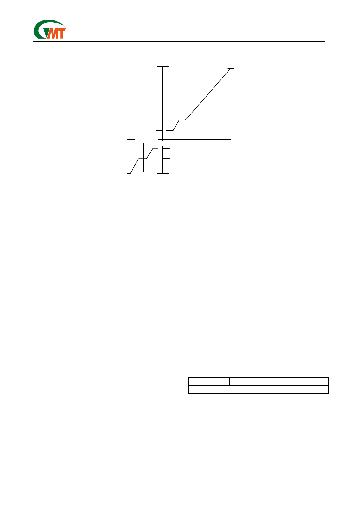
0,1111,1010
Output Code
0,0011,0010
0,0000,0001
0,0000,0000
-25°C
+0.5°C
0°C
-0.5°C
Temperature-to-Digital Transfer Function (Non-linear scale for clarity)
Functional Description
The G751 temperature sensor incorporates a
band-gap type temperature sensor and 9-bit ADC
(Delta-Sigma Analog- to-Digital Converter). The
temperature data output of the G751 is available at
all times via the SMBus. If a conversion is in progress, it will be stopped and restarted after the read.
A digital comparator is also incorporated that compares a series of readings, the number of which is
user-selectable, to user-programmable setpoint and
hysteresis values. The comparator trips the O.S.
output line, which is programmable for mode and
polarity.
O.S. Output, T
and T
OS
HYST
Limits
In Comparator mode the O.S. Output behaves like a
thermostat. The output becomes active when temperature exceeds the T
limit, and leaves the active
OS
state when the temperature drops below the T
limit. In this mode the O.S. output can be used to
turn a cooling fan on, initiate an emergency system
shutdown, or reduce system clock speed. Shutdown
mode does not reset O.S. state in a comparator
mode.
In interrupt mode exceeding T
active but O.S. will remain active indefinitely until
reset by reading any register via the SMBus interface. Once O.S. has been activated by crossing T
then reset, it can activated again only by Temperature going below T
. Again, it will remain active
HYST
indefinitely until being reset by a read. Placing the
G751 in shutdown mode also resets the O.S. output.
also makes O.S.
OS
HYST
OS
,
+25°C
1,1111,1111
1,1100,1110
1,1001,0010
Temperature
+125°C-55°C
Default Modes
G751 always powers up in a known state. G751
power up default conditions are:
1. Comparator mode
2. T
set to 50°C for G751-1, to 80°C for G751-2
OS
3. T
set to 45°C for G751-1, to 75°C for G751-2
HYST
4. O.S. active low
5. Pointer set to “00”; Temperature Register
With these operating conditions G751 can act as a
stand-alone thermostat with the above temperature
settings. Connection to an SMBus is not required.
SMBus Interface
The G751 operates as a slave on the SMBus, so the
SMBCLK line is an input (no clock is generated by
the G751) and the SMBDATA line is a bi-directional
serial data path. According to SMBus specifications,
the G751 has a 7-bit slave address. The four most
significant bits of the slave address are hard wired
inside the G751 and are “1001”. The three least significant bits of the address are assigned to pins
A2-A0, and are set by connecting these pins to
ground for a low, (0); or to +Vs for a high, (1).
Therefore, the complete slave address is:
1 0 0 1 A2 A1 A0
MSB LSB
Ver: 2.4
Nov 26, 2002
TEL: 886-3-5788833
http://www.gmt.com.tw
4
Page 5

Global Mixed-mode Technology Inc.
Shutdown Mode
*
*
*
*
Shutdown mode is enabled by setting the shutdown
bit in the Configuration register via the SMBus. Shutdown mode reduces power supply current to 1 µA
typical. In interrupt mode O.S. is reset if previously
set and is undefined in Compatator mode during
shutdown. The SMBus interface remains active. Activity on the clock and data lines of the SMBus may
slightly increase shutdown mode quiescent current.
T
, T
OS
HYST
from and written to in shutdown mode.
G751
, and Configuration registers can be read
Time
*
*
OS
OS
T
T
HYST
HYST
T
T
O.S.
O.S.
(Comparator Mode)
(Comparator Mode)
O.S.
O.S.
(Interrupt Mode)
(Interrupt Mode)
Time
active lo w.
active lo w.
Shown for O.S. set for
Shown for O.S. set for
Temperature response
Temperature response
*read any register or placed in shut down
*read any register or placed in shut down
Figure1 O.S. Output Temperature Response Diagram
Temperature Data Format
Temperature data can be read from the Temperature,
T
Set Point, and T
OS
written to the T
Set Point, and T
OS
Set Point registers; and
HYST
Set Point reg-
HYST
isters. Temperature data is represented
by a 9-bit, two’s complement word with an LSB
(Least Significant Bit) equal to 0.5°C:
TEMPERATURE
DIGITAL OUTPUT
BINARY HEX
+125°C 0 1111 1010 0FAh
+25°C 0 0011 0010 032h
+0.5°C 0 0000 0001 001h
0°C 0 0000 0000 000h
-0.5°C 1 1111 1111 1FFh
-25°C 1 1100 1110 1CEh
-55°C 1 1001 0010 192h
Fault Queue
A fault queue of up to 6 faults is provided to prevent
false tripping of O.S. when the G751 is used in noisy
environments. The number of faults set in the queue
must occur consecutively to set the O.S. output.
Comparator/Interrupt Mode
As indicated in the O.S. Output Temperature Response Diagram, Figure 1, the events that trigger
O.S. are identical for either Comparator or Interrupt
mode. The most important difference is that in Interrupt mode the O.S. will remain set indefinitely once it
has been set. To reset O.S. while in Interrupt mode,
perform a read from any register in the G751.
O.S. Output
The O.S. output is an open-drain output and does
not have an internal pull-up. A ”high” level will not be
observed on this pin until pull-up current is provided
from some external source, typically a pull-up resistor. Choice of resistor value depends on many system factors but, in general, the pull-up resistor
should be as large as possible. This will minimize
any errors due to internal heating of the G751. The
maximum resistance of the pull up, based on G751
specification for High Level Output Current, to provide a 2V high level, is 30kΩ.
O.S. Polarity
The O.S. output can be programmed via the configuration register to be either active low (default
mode), or active high. In active low mode the O.S.
output goes low when triggered exactly as shown on
the O.S. Output Temperature Response Diagram,
Figure 1. Active high simply inverts the polarity of the
O.S. output.
Ver: 2.4
Nov 26, 2002
5
TEL: 886-3-5788833
http://www.gmt.com.tw
Page 6

Internal Register Structure
Global Mixed-mode Technology Inc.
SMBDATA
SMBDATA
SMBCLK
SMBCLK
Temperature
Temperature
(Read-only)
(Read-only)
Pointer = 00000000
Pointer = 00000000
Interface
Interface
AddressData
AddressData
Pointer Register
Pointer Register
(Selects register for
(Selects register for
communication
communication
Register Select
Register Select
Configuration
Configuration
(Read-write, sets operating
(Read-write, sets operating
Mode)
Mode)
Pointer = 00000001
Pointer = 00000001
G751
TOS Set Point
TOS Set Point
(Read-write)
(Read-write)
Pointer = 00000011
Pointer = 00000011
There are four data registers in the G751, selected
by the Pointer register. At power-up the Pointer is set
to “00”; the location for the Temperature Register.
The Pointer register latches whatever the last location it was set to. In Interrupt Mode, a read from the
G751, or placing the device in shutdown mode, resets the O.S. output. All registers are read and write,
except the Temperature register which is read only.
A write to the G751 will always include the address
byte and the Pointer byte. A write to the Configuration register requires one data byte, and the T
T
registers require two data bytes.
HYST
OS
and
Reading the G751 can take place either of two ways:
If the location latched in the Pointer is correct (most
of the time it is expected that the Pointer will point to
Temperature register because it will be the data
most frequently read from the G751), then the read
can simply consist of an address byte, followed by
retrieving the corresponding number of data bytes. If
the Pointer needs to be set, than an address byte,
pointer byte, repeat start, and another address byte
will accomplish a read.
THYST Set Point
THYST Set Point
(Read-write)
(Read-write)
Pointer = 00000010
Pointer = 00000010
The first data byte is the most significant byte with
most signification bit first, permitting only as much
data as necessary to be read to determine temperature condition. For instance, if the first four bits of the
temperature data indicates an overtemperature condition, the host processor could immediately take
action to remedy the excessive temperatures. At the
end of a read, the G751 can accept either Acknowledge or No Acknowledge from the Master (No Acknowledge is typically used as a signal for the salve
that the Master has read its last byte).
An inadvertent 8-bit read from a 16-bit register, with
the D7 bit low, can cause the G751 to stop in a state
where the SDA line is held low as shown in Figure 2.
This can prevent any further bus communication until
at least 9 additional clock cycles have occurred. Alternatively, the master can issue clock cycles until
SDA goes high, at which time issuing a “Stop” condition will reset the G751.
SMBCLK
SMBCLK
SMBDATA
SMBDATA
Start
Start
by
by
Master
Master
Ver: 2.4
Nov 26, 2002
A2
A2
A1
Address Byte
Address Byte
A1
A0
A0
D15 D14
D15 D14
D13 D12 D11 D10 D9 D8
R/W
R/W
Bit
Bit
Ack
Ack
by
by
G751
G751
D13 D12 D11 D10 D9 D8
Most Si gnifica nt
Most Si gnifica nt
Data Byter
Data Byter
Master but G751 locks S MBDATA low
Master but G751 locks S MBDATA low
D7
D7
Ack
Ack
by
by
Master
Master
Intended Stop b y
Intended Stop b y
D6 D5 D4 D3 D2 D1 D0
D6 D5 D4 D3 D2 D1 D0
Master detects the error
Master detects the error
of its ways
of its ways
Figure 2. Inadvertent 8-Bit Read from 16-Bit Register where D7 is Zero
http://www.gmt.com.tw
6
Stop
Stop
Ack
Ack
Cond
Cond
by
by
by
by
Master
Master
Master
Master
TEL: 886-3-5788833
Page 7

Pointer Register
(Selects which registers will be read from or written to):
P7 P6 P5 P4 P3 P2 P1 P0
0 0 0 0 0 0 Register Select
P0-P1 :Register Select:
P1 P0 REGISTER
0 0 Temperature (Read only) (Power-up default)
0 1 Configuration (Read/W rite)
1 0 T
1 1 TOS (Read/Write)
P2-P7 :Must be kept zero.
Temperature Register
(Read Only):
D15 D14 D13 D12 D11 D10 D9 D8 D7 D6 D5 D4 D3 D2 D1 D0
MSB Bit 7 Bit 6 Bit 5 Bit 4 Bit 3 Bit 2 Bit 1 LSB X X X X X X X
D0-D6 :Undefined
D7-D15 :Temperature Data. One LSB = 0.5°C. Two’s complement format.
Global Mixed-mode Technology Inc.
(Read/Write)
HYST
G751
Configuration Register
(Read/Write):
D7 D6 D5 D4 D3 D2 D1 D0
0 0 0 Fault Queue O.S. Polarity Cmp/Int Shutdown
Power up default is with all bits “0” (zero).
D0 :Shutdown : When set to 1 the G751 goes to low power shutdown mode.
D1 :Comparator / Interrupt mode : 0 is Comparator mode, 1 is Interrupt mode.
D2 :O.S. Polarity : 0 is active low, 1 is active high. O.S. is an open-drain output under all conditions.
D3-D4 :Fault Queue : Number of faults necessary to detect before setting O.S. output to avoid false tripping due
to noise :
D4 D3 NUMBER OF FAULTS
0 0 1 (Power-up default)
0 1 2
1 0 4
1 1 6
D5-D7 :These bits are used for production testing and must be kept zero for normal operation.
T
and TOS Register
HYST
(Read/Write):
D15 D14 D13 D12 D11 D10 D9 D8 D7 D6 D5 D4 D3 D2 D1 D0
MSB Bit 7 Bit 6 Bit 5 Bit 4 Bit 3 Bit 2 Bit 1 LSB X X X X X X X
D0-D6 :Undefined
D7-D15 :T
Or TOS Trip Temperature Data. Power up default is TOS = 50°C /80°C for G751-1/G751-2, T
HYST
HYST
=
45°C /75°C for G751-1/G751-2.
Ver: 2.4
Nov 26, 2002
7
TEL: 886-3-5788833
http://www.gmt.com.tw
Page 8

Global Mixed-mode Technology Inc.
SMBus Timing Diagrams
A1
A1
A2
A0
A2
A0
A1
A1
A2
A0
A2
A0
Start
Start
by
by
Maste r
Maste r
Start
Start
by
by
Maste r
Maste r
1001
1001
Address Byte
Address Byte
1001
1001
Address Byte
Address Byte
G751
1
1
91
91
D3
D3
D4
D4
D2 D1 D0
D7
D7
D5
D6
D6
D7
D7
D5 D4 D3 D2 D1 D0
R/W
R/W
Ack
Ack
by
by
G751
G751
91
91
R/W
R/W
Ack
Ack
by
by
G751
G751
91
91
D5 D4 D3 D2 D1 D0
Most Significant Data B yte
Most Significant Data B yte
1
1
Pointer Byte
Pointer Byte
1
1
Ack
Ack
by
by
Master
Master
9
9
D1 D0
D1 D0
000000
000000
Ack
Ack
by
by
G751
G751
D5
D6
D6
D7
D7
Least Significant Data B yte
Least Significant Data B yteLeast Significant Data B yte
D2 D1 D0
919
919
No Ack
No Ack
by
by
Master
Master
Stop
Stop
Cond
Cond
by
by
Master
Master
919
919
A1
Repeat
Repeat
Start
Start
by
by
Maste r
Maste r
Start
Start
by
by
Maste r
Maste r
1001
1001
Address Byte
Address Byte
1001
1001
Address Byte
Address Byte
A1
A2
A0
A2
A0
R/W
R/W
A1
A1
A2
A0 D1
A2
R/W
A0 D1
R/W
G751
G751
91
91
Ack
Ack
G751
G751
by
by
D6
D6
D7
D7
Ack
Ack
by
by
1
1
D6
D6
D7
D7
D5 D4 D3 D2 D1 D0
D5 D4 D3 D2 D1 D0
Most Significant Data B yte
Most Significant Data B yte
D2
D2
D3
D3
D4
D4
D5
D5
Pointer Byte
Pointer Byte
D7
D7
D6
D6
D7
D7
Ack
Ack
by
by
Master
Master
9
9
D0
D0
Ack
Ack
by
by
G751
G751
Least Significant Data B yte
Least Significant Data B yteLeast Significant Data B yte
Stop
Stop
Cond
Cond
by
by
Master
Master
D3
D3
D4
D4
D2 D1 D0
D5
D5
D2 D1 D0
No Ack
No Ack
by
by
Master
Master
Stop
Stop
Cond
Cond
by
by
Master
Master
Ver: 2.4
Nov 26, 2002
TEL: 886-3-5788833
http://www.gmt.com.tw
8
Page 9

Global Mixed-mode Technology Inc.
Timing Diagrams (Continued)
by
by
Stop
Stop
Cond
Cond
Master
Master
by
by
Master
Master
No Ack
9
9
9
9
1
1
9
9
1
1
9
9
1
1
No Ack
D0
D0
D1
D1
D2
D2
Data Byte
Data ByteData Byte
D3
D3
D4
D4
D5
D5
D6
D6
D7
D7
by
by
Ack
Ack
G751
G751
R/W
R/W
A2 A1 A0
A2 A1 A0
1
1
0
0
0
0
1
1
D0
D0
D1
D1
0
0
0
0
0
0
0
0
0
0
0
0
R/W
R/W
A0
A0
A1
A1
A2
A2
1
1
0
0
0
0
1
1
Address Byte
Address ByteAddress Byte
by
by
Start
Start
Master
Master
Repeat
Repeat
by
by
Ack
Ack
Master
Master
Pointer Byte
Pointer Byte
by
by
Ack
Ack
G751
G751
(a) Typical Pointer Set followed by Immediate Read from Configuration Register
(a) Typical Pointer Set followed by Immediate Read from Configuration Register
Address Byte
Address Byte
9
9
1
1
9
9
1
1
9
9
1
1
G751
by
by
Stop
Stop
Cond
Cond
Master
Master
by
by
Ack
Ack
G751
9
9
by
by
Stop
Stop
Cond
Cond
Master
Master
by
by
Ack
Ack
G751
G751
D0
D0
D1
D1
D2
D2
D3
D3
D4
D4
Configuration Byte
0
0
0
0
0
0
D0
D0
D1
D1
00
00
0
0
0
0
0
0
0
0
R/W
R/W
A0
A0
A2 A1
A2 A1
1
1
0
0
0
0
1
1
Configuration Byte
by
by
Ack
Ack
Master
Master
Pointer Byte
Pointer Byte
(b) Configuration Register Write
(b) Configuration Register Write
by
by
Ack
Ack
G751
G751
Address Byte
Address Byte
1
1
9
9
1
1
9
9
1
1
9
9
1
1
G751
D0
D0
D5 D4 D3 D2 D1
D5 D4 D3 D2 D1
D6
D6
D7
D7
D0
D0
D1
D1
D2
D2
D3
D3
D4
D4
D5
D5
D6
D6
D0
D0
D1
D1
0
0
0
0
00
00
0
0
0
0
R/W
R/W
A0
A0
A1
A1
A2
A2
1
1
0
0
0
0
Least Significant Data Byte
Least Significant Data ByteLeast Significant Data Byte
by
by
Ack
Ack
G751
G751
Write
Write
Most Significant Data Byte
Most Significant Data Byte
HYST
HYST
D7
D7
by
by
Ack
Ack
by
by
Ack
Ack
1
1
and T
and T
OS
Master
Master
OS
(c) T
(c) T
Pointer Byte
Pointer Byte
G751
G751
Address Byte
Address Byte
Ver: 2.4
Nov 26, 2002
by
by
by
Start
Start
Master
Master
by
by
Start
Start
Master
Master
by
Start
Start
Master
Master
TEL: 886-3-5788833
http://www.gmt.com.tw
9
Page 10

Global Mixed-mode Technology Inc.
Package Information
°
7
(4X)
G751
C
E
H
L
D
θ
A2
A
y
e
B
A1
8 Pin SOP Package
Note:
1. Package body sizes exclude mold flash and gate burrs
2. Dimension L is measured in gage plane
3. Tolerance 0.10mm unless otherwise specified
Controlling dimension is millimeter converted inch dimensions are not necessarily exact.
4.
SYMBOL
A 1.35 1.60 1.75 0.053 0.063 0.069
A1 0.10 ----- 0.25 0.004 ----- 0.010
A2 ----- 1.45 ----- ----- 0.057 -----
B 0.33 ----- 0.51 0.013 ----- 0.020
C 0.19 ----- 0.25 0.007 ----- 0.010
D 4.80 ----- 5.00 0.189 ----- 0.197
E 3.80 ----- 4.00 0.150 ----- 0.157
e ----- 1.27 ----- ----- 0.050 -----
H 5.80 ----- 6.20 0.228 ----- 0.244
L 0.40 ----- 1.27 0.016 ----- 0.050
y ----- ----- 0.10 ----- ----- 0.004
θ
MIN. NOM. MAX. MIN. NOM. MAX.
0º ----- 8º 0º ----- 8º
DIMENSION IN MM DIMENSION IN INCH
Ver: 2.4
Nov 26, 2002
10
TEL: 886-3-5788833
http://www.gmt.com.tw
Page 11

Global Mixed-mode Technology Inc.
8
8
E
E
E1
E1
1
C0.076
C0.076
SEATING PLANE
SEATING PLANE
WITH PLATING
WITH PLATING
BASE METAL
BASE METAL
1
e
e
A2
A2
b
b
D
D
c1
c1
b1
b1
b
b
A
A
A1
A1
GAUGE PLANE
GAUGE PLANE
c
c
DETAIL “A”
DETAIL “A”
0.25
0.25
θ
θ
R1
R1
R
R
G751
AA
AA
C
C
L
L
2
2
θ
θ
3
3
θ
L
L
1
1
θ
8 Pin MSOP Package
SYMBOL
MIN. NOM. MAX. MIN. NOM. MAX.
A ----- ----- 1.10 ----- ----- 0.043
A1 0.05 ----- 0.15 0.002 ----- 0.006
A2 0.81 0.86 0.91 0.032 0.034 0.036
b 0.25 ----- 0.40 0.008 ----- 0.012
b1 0.25 0.30 0.35 0.010 0.012 0.014
c 0.13 ----- 0.23 0.005 0.009
c1 0.13 0.15 0.18 0.005 0.006 0.007
D 2.90 3.00 3.10 0.114 0.118 0.122
E1 2.90 3.00 3.10 0.114 0.118 0.122
e 0.65 BSC 0.026 BSC
E 4.90 BSC 0.193 BSC
L 0.445 0.55 0.648 0.0175 0.0217 0.0255
1
θ
θ
θ
2
3
0° ----- 6° 0
R 0.09 ----- ----- 0.004 ----- ----R1 0.09 ----- ----- 0.004 ----- -----
JEDEC MO-187AA
DIMENSION IN MM DIMENSION IN INCH
----- 6°
°
12 REF 12 REF
12 REF 12 REF
Taping Specification
Feed Direction
Feed Direction
Typical SOP/MSOP Package Orientation
Typical SOP/MSOP Package Orientation
GMT Inc. d oes not assume any responsibility for use of any circuitry described, no circuit patent licenses are implied and GMT Inc. reserves the right at any time without notice to change said circuitry and specifications.
Ver: 2.4
Nov 26, 2002
11
TEL: 886-3-5788833
http://www.gmt.com.tw
 Loading...