

Page 1

IMAGE SENSORS
FXA 1012
Frame Transf er CCD Image Sensor
Objective specification 2000 January 7
File under Image Sensors
Philips
Semiconductors
Page 2

Philips Semiconductors Objective specification
g
Frame Transfer CCD Image Sensor FXA 1012
• 2M active pixels (1616H x 1296V)
• 2/3-inch type optical format
• Still and monitor modes
• RGB Bayer pattern colour filter s
• Progressive scan
• Excellent anti-blooming (V ertical Overflow
Drain)
• High dynamic range (>70dB)
• High sensitivity
• Low dark current and low fixed pattern noise
• Low read-out noise
• V ariable electr onic shuttering
• Data rate up to 25 MHz, 5 frames/s
• Small outline LCC package
• Low cost
Device structure
Optical size: 8.16 mm (H) x 6.53 mm (V)
Chip size: 9.49 mm (H) x 9.32 mm (V)
Pixel size: 5.1 µm x 5.1 µm
Active pixels: 1616 (H) x 1296 (V)
Total no. of pixels: 1688 (H) x 1324 (V)
Optical black pixels: Left: 2 Right: 70
Optical black lines: Top: 12 Bottom: 12
Total no. of storage lines: 298
Dummy register cells: 8
Description
The FXA 1012 is a colour frame-transfer CCD image sensor designed
for consumer digital photography applications. The combination of
high speed and a high linear dynamic range of over 10 true bits
makes this device the perf ect solution for use in compact high quality
imaging applications. Two modes of operation provide both a
monitoring image for LCD screens, and a full resolution, zero-smear
still image with excellent colour rendition. The device structure is
shown in figure 1.
12 dark lines
8 black lines
Image
Section
1616 active pixels
12 dark + 4 dummy lines
Storage Section
298 lines x 1688 cells
1688 cells
Output re
ister
GBGB
RGRG
GBGB
1296
active
lines
GBGB
RGRG
70
Output
amplifier
8
GBGB
RGRG
GBGB
2
GBGB
RGRG
Figure 1 - Device structure
2000 January 2
Page 3

Philips Semiconductors Objective specification
Frame Transfer CCD Image Sensor FXA 1012
Architecture of the FXA 1012
The FXA 1012 consists of an open image section and a storage
section with an optical light shield. An output register and amplifier
are located below the storage section for read-out.
The optical centres of all pixels in the image section form a square
grid. The image area has RGB Bay er colour filter pattern. The charge
is generated and integrated in the image section. This section is
controlled by four image cloc k phases (A1 to A4). After the integration
time the image charge is shifted one line at a time to the storage
section.
The storage section is controlled by four storage clock phases (B1
to B4). In the still mode the image inf ormation is transported straight
IMAGE SECTION
Image diagonal (active video only)
Aspect ratio
Active image width x height
Pixel width x height
Image clock pins
Capacity of each clock phase
Number of active lines
Number of black reference lines
Number of dummy lines
Total number of lines
Number of active pixels per line
Number of black reference pixels per line
Total number of pixels per line
10.4 mm
5:4
8.24 x 6.61 mm
5.1 x 5.1 µm
A1, A2, A3, A4
5.4 nF per pin
1296
24 (12+12)
4
1324
1616
72 (2+70)
1688
through the storage section to the horizontal output register. In the
monitoring mode subsampling of the image is performed at the
image-to-storage transition and the subsampled image is stored in
the storage section. The stored image is shifted one line at a time
into the horizontal output register.
In the next active line time the pixels are transpor ted towards the
output amplifier. Four clock phases (C1 to C4) control the pixel
transport in the output register. In the output amplifier the charge
packets are dumped one by one on a floating diffusion area. The
voltage of this area is sensed and buffered by a three-stage FET
source-follower. Figure 2 shows the detailed internal structure.
2
2
STORAGE SECTION
Cell width x height
Storage clock pins
Capacity of each clock phase
Number of cells per line x number of lines
5.1 x 5.1 µm
B1, B2, B3, B4
1.5 nF per pin
1688 x 298
2
OUTPUT REGISTER
Number of dummy cells
Total number of register cells
Output register clock pins
Capacity of each clock phase
Reset Gate (RG) capacity
Output stage
8
1696
C1, C2, C3, C4
60 pF per pin
15 pF
3-stage source follower (open source)
2000 January 3
Page 4

Philips Semiconductors Objective specification
Frame Transfer CCD Image Sensor FXA 1012
Operational modes
The FXA 1012 is designed for high-resolution digital photography
with real time monitoring at reduced resolution. T w o diff erent modes
of operation make this possible.
In the still picture mode the high-resolution image is read-out directly .
A mechanical shutter ensures a 100% smear-free image with a
resolution of 1600 (H) x 1280 (V).
A1
A2
A3
A4
12 lines
1296 active
images
lines
16 lines
OG: output gate
RG: reset gate
One Pixel
A1
A2
A3
A4
A1
A2
A3
A4
A1
A2
A3
A4
A1
A2
A3
A4
A1
A2
A3
A4
B1
B2
B3
B4
RD: reset drain
B1
B2
B3
OUT
RG
RD
OG
8 dummy pixels
B4
C4C2 C1C3C4C2 C1C3 C4C2 C1C3C4C2 C1 C4C2 C1C3 C4C2 C1C3 C4C2 C1C3 C4C2 C1C3 C4C2 C1C3 C4C2 C1C3
column
1
2 black timing
columns
298 storage
lines
column
2+1
1616 image pixels
In the monitoring mode, images with reduced vertical resolution are
produced that are suitable for LCD displa ys. These images can hav e
for example, 120, 240 or 256 lines at up to 40 images per second.
A1
A2
A3
A4
A1
A2
A3
A4
A1
A2
A3
A4
IMAGE
FT CCD
STORAGE
column
2+1616
70 black timing columns
A1
A2
A3
A4
A1
A2
A3
A4
A1
A2
A3
A4
B1
B2
B3
B4
B1
B2
B3
B4
column
2+1616+70
A1, A2, A3, A4: clocks of image section
B1, B2, B3, B4: clocks of storage section
C1, C2, C3, C4: clocks of horizontal register
Figure 2 - Detailed internal structure
2000 January 4
Page 5

Philips Semiconductors Objective specification
Frame Transfer CCD Image Sensor FXA 1012
Specifications
Absolute Maximum Ratings Min. Max. Unit
GENERAL:
storage temperature
ambient temperature during operation
voltage between any two gates
DC current through any clock phase (absolute value)
OUT current (no short circuit protections)
VOLTAGES IN RELAT ION TO VPS:
VNS, RD
all other pins
VOLTAGES IN RELAT ION TO VNS:
RD
VPS
all other pins
-40
-20
-20
-0.2
0
-0.5
-10
-10
-30
-30
+80
+60
+20
+2.0
4
+30
+25
+0.5
+0.5
+0.5
°C
°C
V
µA
mA
V
V
V
V
V
Max. current
[mA]
2
2
2
3
5.5
1
-
-
VNS
VPS
SFD
SFS
OG
RD
1
N substrate
P substrate
Source Follower Drain
Source Follower Source
Output Gate
Reset Drain
DC Conditions Min. [V] Typical [V] Max. [V]
20
6
19
0
3.5
19
24
7
20
0
4
20
28
9
21
0
4.5
21
Min. Typical Max. Pin
Number of adjustments 0 0 1 VNS
1
To set the VNS voltage for optimal Anti-Blooming (vertical overflow drain), it should be adjustable between minimum and maximum values.
2
Currents INS and IPS are specified at overexposure of 100 x Qmax.
3
Measured with Rload = 3.3 kOhms.
AC Clock Level Conditions Min. Typical Max. Unit
IMAGE CLOCKS:
A-clock amplitude
A-clock low level
11 12
0
13 V
V
STORAGE CLOCKS:
B-clock amplitude
B-clock low level
11 12
0
13 V
V
HORIZONTAL AND RESET CLOCKS:
C-clock amplitude
C-clock low level C1, C3
C-clock low level C2, C4
Reset Gate (RG) amplitude
Reset Gate (RG) high level
4.5
2.5
4.5
21
5
0
3
5
22
5.5
3.5
5.25
23
VNS PULSE:
Charge Reset (CR) pulse on VNS 4.5 5 5.5 V
2000 January 5
V
V
V
V
V
Page 6
Philips Semiconductors Objective specification
Frame Transfer CCD Image Sensor FXA 1012
Timing diagrams (for default operation)
AC Characteristics Min. Typical Max. Unit
Horizontal frequency
Vertical frequency
Charge Reset (CR) time
Rise and fall times: image clocks (A)
register clocks (C)
reset gate (RG)
1
Typical value for monitor mode.
2
Duty cycle = 50%
3
Tp is pulse period of C clocks
C-clock pulses
FREQUENCY = 25 MHz
SSC
C1
C2
C3
C4
RG
blue (even) lines
red (odd) lines
8 dummy pixels
2
black 1600 active pixels within aspect ratio
pixels
10
2
10
3
3
COMPLETE LINE READOUT CYCLE
8 overscan pixels
RG G RGR
GBGB
RGR
C1
C2
G
GB
RG
20ns
G
R
6ns
G
B
BG BG
R
GRG
25MHz HORIZONTAL TRANSPORT PULSES
40ns
1616 active pixels
BGGBGBG G
....
..
.
..
..
.
.
.
G
1.56
12
20
5
5
GRG
8 overscan pixels
G
B
RGR
1
BGB
R
25
MHz
MHz
14
3
Tp/8
Tp/8
70 black pixels
BB
G
RG
µs
ns
ns
ns
C3
C4
RG
SENSOR SIGNAL
6.7ns
Figure 3 - Timing diagram for horizontal pulses
2000 January 6
Page 7

Philips Semiconductors Objective specification
Frame Transfer CCD Image Sensor FXA 1012
HORIZONTAL PULSES
C-clock frequency = 25MHz
Thorizontal = 1/25E6 * 2040 = 81.6us
1600 active pixels
phase count
SSC
CR_A1/A2
CR_NS
A1 / B1
A2 / B2
A3 / B3
A4 / B4
1696 sensor pixels
1960
1940
Line shift
Line shift
Line shift
Line shift
2020
2040/0
31 dummy
black
20
312 lineblanking
60
80
40
49
49
49
100
140
120
129
109
180
160
12 us
169
149
18989
240
220
200
8 overscan
1980
70 black
2000
Figure 4 - Pulse timing diagrams for vertical clocks during line blanking
2 black
8 dummy
8 overscan
phiC reg
300
320
280
260
34069360
349
349
36148
1600 active pixels
380
400
440
420
STILL PICTURE MODE - 1/30s Integration
Tvertical = (1/25E6 * 2040) * 2035 = 166.1 ms
298
storage lines
integration
line count
NS_pulse
A1 / A2
A3 / A4
B1 / B2
B3 / B4
2028
2029
2030
2031
2032
2033
2035/0
12345
2
678
9
292
293
291
1622 sensor lines
4
dummy
294
295
296
297
298
301
300
299
12 1281280
302
303
304
305
306
307
308
309
310
311
8
overscan
316
322
317
318
319
320
315
314
line shift
321
313
312
1324
image lines
active lines
327
325
324
323
328
326
Figure 5 - Still picture mode timing diagrams
1599
1600
1601
1602
1603
1604
1605
4
dummy
lines
1622
1623
1624
1626
1625
1626
1628
1628
CR
CR
integration
1627
1628
1629
1630
1631
1632
overscan black linesblack lines
1615
1612
1606
1609
1610
1611
1507
1608
1613
1614
1616
1617
1618
1619
1620
1621
2000 January 7
Page 8

Philips Semiconductors Objective specification
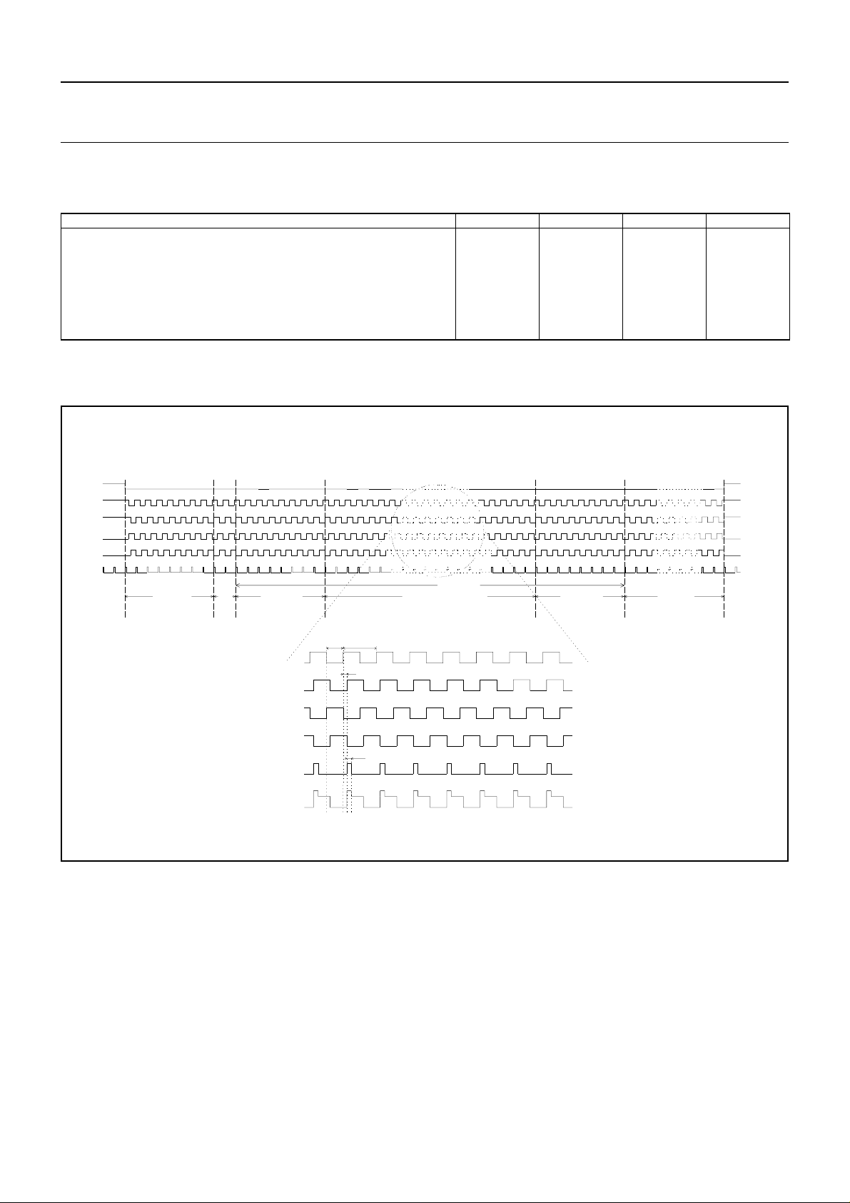
MONITOR MODE
1/60s int
FS
Frame Transfer CCD Image Sensor FXA 1012
-
Tvertical = (1/25E6 * 2040) * 315 = 25.7ms
314
315/0
2
1
1
2
2
2
2
3456789
frame shift line shift
line count
NS_pulse
A1 / A2
A3 / A4
B1 / B2
B3 / B4
and Subsampling pulses in monitor mode
4 phase - 4:4 Frame Shift with 2/10 subsampling
Transport frequency 1.56MHz
FS-counter
A1
A2
A3
A4
B1
B2
B3
B4
111213141516171819
10
4 dummy 12 black 1290 active image lines to 258 lines via subsampling
213
egration
4
4
dummy
dummyblack
14
18
567891011
4
20
12
black
24252627282930
232221
121314
31
323334
15
integration
298 sensor lines
264
subsampled
110
111
112
CR
113
CR
113
12
black
298
299
300
301
113
114
295
296
302
297
303
304
remaining storage lin
305
306
307
308
6
309
310
311
312
313
314
315/0
1
1
315
18
16
17
202122
19
2425262728
23
29
303132
3334353637
38
FS-counter
A1
A2
A3
A4
B1
B2
B3
B4
1293
1294
1295
1296
1297
1298
1299
1300
1301
1302
Remaining 6 active image lines
1313
1311
1303
1304
1305
1306
1307
1308
1309
1310
1312
1314
1315
1316
Figure 6 - Monitor mode timing diagrams
12 black Removing 6 storage gap lines
1325
1326
1317
1318
1319
1320
1321
1322
1323
1324
1327
1328
1329
1330
2000 January 8
Page 9

Philips Semiconductors Objective specification
Frame Transfer CCD Image Sensor FXA 1012
Pixel timing
C1
C2
C3
C4
RG
Y : 5V/ Div. X : 10ns/ Div.
Figure 7 - Start horizontal readout
—> time
2000 January 9
Page 10

Philips Semiconductors Objective specification
Frame Transfer CCD Image Sensor FXA 1012
Performance
The test conditions for the perfor mance characteristics in the still
mode of operation are as follows:
• All values are measured using typical operating conditions.
• Integration time = 1/30 sec (unless specified otherwise).
• Test temperature = 60°C (333K).
Performance Characteristics Min. Typical Max. Unit
• The light source is a 3200K lamp with a 1.7mm thick BG40 infrared
cut-off filter; F=16.
• Vertical Anti-Blooming condition
• Horizontal transport frequency = 25MHz.
Charge Transfer Efficiency 1 vertical
Charge Transfer Efficiency
1
horizontal
Image lag
Sensitivity, green S
Sensitivity, red SR
Sensitivity, blue SB
Sensitivity Ratio SG / S
Sensitivity Ratio SG / S
Sensitivity Ratio SR / S
Shading per colour plane
Differential colour shading
2
G
2
2
R
B
B
3
4
PRNU per colour plane
Green–green difference
Power consumption (Still mode)
5
40
Power consumption (Monitoring mode)
Full-well capacity saturation level (Q
Saturation signal
Dynamic range at 20°C : 20log(Q
Overexposure
1
Charge Transfer Efficiency values are expressed as the value per gate transfer.
2
The sensitivity when a light source directly illuminates the CCD.
3
Shading is defined as the one-σ value of the pixel output distribution expressed as a percentage of the mean value output (low-pass image).
4
Difference in shading between the four colour planes, with standard imaging condition, still mode.
5
Difference in average green signal between ‘green in red line’ and ‘green in blue line’, with standard imaging condition, still mode
6
Q
is determined from the lowpass filtered image.
max
7
Overexposure over entire area while maintaining good Ver tical Anti-Blooming (VAB). It is tested by measuring the dark line.
7
handling
6
)
max
/noise electrons)
max
35
720
0.999997
0.999997
295
240
175
1.25
1.7
1.4
2
0.8
50
45
1000
72
100
0
2.5
5
60
55
1500
%
mV/lux.s
mV/lux.s
mV/lux.s
%
%
%
%
mW
mW
3
x 10
mV
dB
x Q
level
max
2000 January 10
Page 11

Philips Semiconductors Objective specification
*
Frame Transfer CCD Image Sensor FXA 1012
RGB response
100
90
80
70
60
50
40
30
Response (A.U.)
20
10
0
400 450 500 550 600 650 700
*Arbitrary units
Output Buffer Min Typical Max Unit
Conversion factor at output node
Supply current
Bandwidth
RMS readout noise @ 5MHz bandwidth after CDS
Blue
Green
Waveleng ht (nm)
Figure 8 - RGB response
18 20
Red
4
95
12
25
15
µV/el.
mA
MHz
el.
Dark Condition at 60
Average no. of dark signal electrons per pixel aft er 1/30 sec integrat i o n
Dark signal shading
Dark current level @ 60° C
Fixed Pattern Noise
1
Typical operating conditions (Image capture mode; 60°C; 1/30s exp. time).
2
FPN is the one-σ value of the highpass image.
2
(FPN) @ 60° C
1
C
°°°°
Min. Typical Max. Unit
25
1
0.3
15
0.6
25
electrons
mV
nA/cm
electrons
2
2000 January 11
Page 12

Philips Semiconductors Objective specification
Frame Transfer CCD Image Sensor FXA 1012
Application information
Current handling
One of the purposes of VPS is to drain the holes that are generated
during exposure of the sensor to light. Free electrons are either
transported to the VRD connection and, if excessive (from overexposure), free electrons are drained to VNS. No current should
flow into VPS. During overexposures a total current 0.5 to 1mA
through VPS ma y be expected. The PNP emitter f ollower in the circuit
diagram (figure 9) serves these current requirements.
VNS drains superfluous electrons as a result of overexposure. In
other words, it only sinks current. During overe xposures a total current
of 0.5 to 1mA through VNS may be expected. The NPN emitter
follower in the circuit diagram meets these current requirements.
The clamp circuit, consisting of the diode and electrolytic capacitor,
enables the addition of a Charge Reset (CR) pulse on top of an
otherwise stable VNS voltage. To protect the CCD, the current
resulting from this pulse should be limited. This can be accomplished
by designing a pulse generator with a rather high output impedance.
a current source or more simply with a resistance to GND. In order
to prevent the output (which typically has an output impedance of
about 400 Ohm) from bandwidth limitation as a result of capacitive
loading, load the output with an emitter follower built from a highfrequency transistor. Mount the base of this transistor as close as
possible to the sensor and keep the connection between the emitter
and the next stage short. The CCD output buffer can easily be
destroyed by ESD. By using this emitter follower, this danger is
suppressed; do NOT reintroduce this danger by measuring directly
on the output pin of the sensor with an oscilloscope probe. Instead,
measure on the output of the emitter follower. Slew rate limitation is
prevented by avoiding a too-small quiescent current in the emitter
follower; about 10mA should do the job. The collector of the emitter
follower should be decoupled properly to suppress the Miller effect
from the base-collector capacitance. A CCD output load resistor of
3.3 kΩ typically results in a bandwidth of 95MHz.
Decoupling of DC voltages
All DC voltages (not VNS, which has additional CR pulses as
described above) should be decoupled with a 100nF decoupling
capacitor. This capacitor must be mounted as close as possible to
the sensor pin. Further noise reduction (by bandwidth limiting) is
achieved by the resistors in the connections between the sensor
and its voltage supplies. The electrons building up the charge pac kets
that will reach the floating diffusion only add up to a small current,
which will flow through VRD. Therefore a large series resistor in the
VRD connection may be used.
Output
To limit the on-chip power dissipation, the output buffer is designed
with open source output. The output should theref ore be loaded with
B1
B2
VNS
A4
NC
B1
BAT74
BAT74
C4
3K3
B2
VPS
NC
OUT
SFD
100n
BAT74
SFS RD RG
R3
22K
100K
BC860C
47K
R9
100E
R7
R8
2K2
CCD OUT
VSFD
C1
Cstray
47E
R6
100n
R1
R2
BFR92
From V-Drivers From PPGFrom CCD Supply
A3
A4
A3
FXA 1012
C6
100n
Device protection
The output buffer or VNS of the FXA 1012 is likely to be damaged if
VPS rises above SFD or RD at any time. This danger is most realistic
during power-on or power-off of the camera.
Never exceed the maximum output current. This may damage the
device permanently. The maximum output current should be limited
to 6mA. Be especially aware that the output buffers of these image
sensors are very sensitive to ESD damage.
Because of the fact that our CCDs are built on an n-substrate, we
are dealing with some parasitic NPN transistors. To avoid activation
of these transistors during switch-on and switch-off of the camera,
we recommend the application diagram of figure 9.
3
2
1
4
A2
A2 A1
C4
A1
B3
B4
ES
NC
B3
4.7uF
B4
VNS
NC
OG
C3
C2
C1
C2
1K
R5
BAS28
C3
R4
47K
100n
C5
C7
100n
C8
100n
C9
100n
100n
100K
H DRIVER
R18
1
G
R
C
C
C
C
R11
100K
R14
22K
Figure 9 - Application diagram to protect the FXA 1012
2000 January 12
R15
100K
BAS28
BAS28
R16
6K8
R12
100K
R17
18K
BAS28
100nC11100nC10
R13
100K
74ACT04
Page 13

Philips Semiconductors Objective specification
Frame Transfer CCD Image Sensor FXA 1012
Peripheral ICs
To allow compact and low-cost applications, use of the following
peripheral circuits for the FXA 1012 is suggested:
• Pulse Patter n Generator
The PPG (pulse pattern generator) delivers all the pulses, at logic
level, to drive the ver tical clocks of the CCD. For this sensor, the
PPG is included in the DSP SAA8122 or separately in the Timing
Generator SAA8103.
• Vertical Drivers + DC/DC Converter
The vertical drivers convert the 3.3V or 5V logic pulses from the
PPG to 12V analog pulses to drive the vertical clocks of the CCD.
The recommended driver is the Philips TDA9991.
• CDS - AGC - ADC
The combined CDS (correlated double sampling) - AGC (automatic
gain control) and ADC (10 bit analog-to-digital convertor) is the
easiest way to link the output of the CCD to a DSP (digital signal
processor). Philips Semiconductors # TDA8783
• DSP
A dedicated DSP has been developed that can handle the image
format and different modes of the FXA 1012. Philips
Semiconductors # SAA8122.
Special modes of operation
Monitor mode with 240 lines vertical resolution is achieved with 1:5
subsampling, yielding 1200/5 = 240 lines. When 1:4 subsamlping is
applied, an image with 288 lines vertical resolution is obtained.
Device Handling
An image sensor is a MOS device which can be destroy ed by electrostatic discharge (ESD). Therefore, the device should be handled
with care.
Always store the device with short-circuiting clamps or on conductive
foam. Alwa ys s witch off all electric signals when inserting or removing
the sensor into or from a camera (the ESD protection in a CCD
image sensor is less effective than the ESD protection of standard
CMOS circuits).
Being a high quality optical device, it is important that the cover
glass remain undamaged. When handling the sensor , use fingercots.
T o remo ve the protectiv e tape from the cov er glass, use the f ollowing
procedure:
• do not scratch or tear off the protective tape before mounting.
• peel off the tape slowly.
• the use of an ionised air blow er is recommended when peeling off
the tape.
• once peeled off, do not reuse the tape.
To clean stains from the package surface, use a cotton stick soak ed
in ethanol. Wipe carefully in order not to scratch the glass surface.
Dry rubbing of the cover glass may cause electro-static discharges
which can destroy the device.
Soldering information
The CCD package temperature must not exceed 150°C. Soldering
iron temperature should be under 300°C when mounting a CCD on
a printed circuit board. Aim for a solder ing time of 3 seconds per
pad. Use a soldering iron that has an adjustab le temperature control
function (that is grounded) that holds the soldering iron tip at a
constant temperature.
2000 January 13
Page 14

Philips Semiconductors Objective specification
Frame Transfer CCD Image Sensor FXA 1012
Pin configuration
Pin Number Symbol
1
2
3
4
5
6
7
8
9
10
11
12
4
a3
a4
NC
b1
b2
vps
NC
out
sfd
sfs
rd
rg
123 242322
Pin Number Symbol
13
14
15
16
17
18
19
20
21
22
23
24
21
21
c4
c1
c2
c3
og
NC
vns
b4
b3
NC
a1
a2
123242322
4
5
6
7
8
9
10 11 12 13 14 15
20
19
18
17
16
Figure 10 - Pin configuration
20
19
18
17
16
13 12 11 101415
5
6
7
8
9
2000 January 14
Page 15

Philips Semiconductors Objective specification
Frame Transfer CCD Image Sensor FXA 1012
Pack age inf ormation
16. 3 +/ - 0. 2
14. 1 +/ - 0. 4
8. 605 +/ - 0. 2
0. 3 +/ - 0. 13
Optical center
8. 3 +/ - 0. 2 8. 3 +/ - 0. 2
6. 3 +/ - 0. 4 6. 4 +/ - 0. 4
R0.5
a
(R0.6)
1. 865 +/ - 0. 2
12. 7 +/ - 0. 1
2. 54
Glass
1. 2 +/ - 0. 15
Resin
V
H
1. 2
1. 685 +/ - 0. 168
2. 05 +/ - 0. 14
3. 55 +/ - 0. 2
1+/-0.1
B
a-a'
2. 9 +/ - 0. 4
1
(1.2)
2- 1
c
1. 2
a'
A
Sensor
0. 7 +/ - 0. 08
4-R0.3
R0.25
1. The bottom of the package [A] is the height reference.
2. The height from the bottom [A] to the effective image area is 1.685 +/-0.168mm.
The height from the top of the cover glass [B] to the effective image area is 1.865 +/-0.2mm.
3. The tilt of the effective image area relative to the height reference is less than 0.095mm.
4. The thickness of the Au plating is more than 1.0um.
The thickness of the Au plating is less than 3.0um.
5. The point [C] is the origin of H&V direction.
6. The center of effective image area relative to [C] is (V,H)=(8.605,0)+/-0.2mm.
7. The rotation angle of the effective image area relative to H and V is less than +/-1.5 degrees.
8. The rotation angle of the cover glass relative to H and V is less than +/-2degrees.
9. The thickness of the cover glass is 1.5 +/-0.05mm, and the refractive index 1.5.
10. The refractive index of the resin is 1.5.
11. The tolerances that are not shown are +/-0.13mm.
12. D=2.18 +/-0.44mm
D: Distance between left edge of imaging area and left edge of cover glass.
+/-0.44mm means 4sgm = 0.44mm.
13. No horizontal force is allowed to cover glass lid.
ALL LINEAR DIMENSIONS ARE IN MILLIMETERS
Figure 11 - Mechanical drawing of the FXA 1012 package
2000 January 15
Page 16

Philips Semiconductors Objective specification
Frame Transfer CCD Image Sensor FXA 1012
13. 5
6. 7
2
R
a
a'
Protection foil
Glass
Resin
12
14. 5
Sensor
0. 06
a-a'
Figure 12 - Protective foil on top of cover glass
2000 January 16
Page 17

Philips Semiconductors Objective specification
Frame Transfer CCD Image Sensor FXA 1012
Order codes
The sensor can be ordered using the following code:
FXA 1012 sensor
Description Order Code
FXA 1012 WC 9352 670 10117
You can contact the Image Sensors division of Philips
Semiconductors at the following address:
Philips Semiconductors
Image Sensors
Internal Postbox WAG-05
Prof. Holstlaan 4
5656 AA Eindhoven
The Netherlands
phone +31 - 40 - 27 44 400
fax +31 - 40 - 27 44 090
www.semiconductors.philips.com/imagers/
Philips reserves the right to change any information contained herein without notice. All information furnished by Philips is believed to be accurate. © Philips Electronics N.V. 2000
9352 670 10117
Philips
Semiconductors
 Loading...