

Page 1
CML Semiconductor Products
TETRA Baseband Processor FX980
1997 Consumer Microcircuits Limited
D/980/3 November 1997
1.0 Features Advance Information
•• RRC Filters for both Tx and Rx •• 4 x10-Bit D-A and 4 Input 10-Bit A-D
•• ππ/4 DQPSK Modulation
•• Transmit Output Power Control
•• 2x 13-Bit Resolution Sigma Delta D-A •• Low Power 3.0 - 5.5Volt Operation
•• 2x 16-Bit Resolution Sigma Delta A-D •• Effective Power down Modes
1.1 Brief Description
This device is intended to act as an interface between the analogue and digital sections of a Digital Radio
System, and performs many critical and DSP-intensive functions. The chip is designed with the necessary
capability to meet the requirements for use in both mobile and base station applications in Terrestrial Trunked
Radio (TETRA) systems.
The transmit path comprises all the circuitry required to convert digital data into suitably filtered analogue I
and Q signals for subsequent up-conversion and transmission. This includes digital control of the output
amplitudes, digital control of the output offsets and fully programmable digital filters: default coefficients
provide the RRC response required for TETRA.
The receive section accepts differential analogue I and Q signals at baseband and converts these into a
suitably filtered digital form for further processing and data extraction. A facility is provided for digital offset
correction and the digital filters are fully programmable with default coefficients providing the RRC response
required for TETRA.
Auxiliary DAC and ADC functions are included for the control and measurement of the RF section of the radio
system. This may include AFC, AGC, RSSI, or may be used as part of the control system for a Cartesian
Loop.
Page 2

TETRA Baseband Processor FX980
1997 Consumer Microcircuits Limited 2 D/980/3
CONTENTS
Section Page
1.0 FEATURES.......................................................................................................................................1.
1.1 BRIEF DESCRIPTION.......................................................................................................................1
1.2 BLOCK DIAGRAM............................................................................................................................3
1.3 SIGNAL LIST....................................................................................................................................4
1.4 EXTERNAL COMPONENTS.............................................................................................................6
1.5 GENERAL DESCRIPTION................................................................................................................7
1.5.1 Connection and Decoupling of Power Supplies...................................................................7
1.5.2 Tx Data Path............................................................................................................................8
1.5.2.1 Modulator..............................................................................................................................8
1.5.2.2 Filters....................................................................................................................................8
1.5.2.3 Gain Multiplier........................................................................................................................8
1.5.2.4 Offset Adjust..........................................................................................................................8
1.5.2.5 Sigma-Delta D-A Converters and Reconstruction Filters.........................................................8
1.5.2.6 Phase Pre-distortion...............................................................................................................8
1.5.2.7 Ramping Output Amplitude....................................................................................................8
1.5.3 Rx Data Path............................................................................................................................9
1.5.3.1 Anti-Alias Filtering and Sigma-Delta A-D Converters..............................................................9
1.5.3.2 Filters.....................................................................................................................................9
1.5.3.3 Offset Registers.....................................................................................................................9
1.5.3.4 I and Q Channel Gain.............................................................................................................9
1.5.4 Auxiliary Circuits....................................................................................................................9
1.5.4.1 10-Bit DACs...........................................................................................................................9
1.5.4.2 10-Bit ADC.............................................................................................................................9
1.5.4.3 Power Ramping and Control.................................................................................................10
1.5.5 IRQ Function.........................................................................................................................10
1.5.6 Serial Interface......................................................................................................................10
1.5.6.1 Command Interface..............................................................................................................11
1.5.6.2 Command Read Interface....................................................................................................12
1.5.6.3 Rx Data Interface.................................................................................................................12
1.5.6.4 Transmission of Data...........................................................................................................12
1.5.6.5 Command Control Serial Word.............................................................................................13
1.5.7 Register Description.............................................................................................................14
1.5.7.1 Register and Access Point Summary...................................................................................16
1.6 APPLICATION NOTES...................................................................................................................33
1.6.1 General...................................................................................................................................33
1.6.2 Transmitter.............................................................................................................................33
1.6.3 Receiver.................................................................................................................................33
1.6.4 Timing.....................................................................................................................................33
1.7 PERFORMANCE SPECIFICATION.................................................................................................33
1.7.1 Electrical Performance............................................................................................................33
1.7.2 Packaging...............................................................................................................................33
Note: As this product is still in development, it is likely that a number of changes and additions will be made
to this specification. Items marked TBD or left blank will be included in later issues. Information in this
data sheet should not be relied upon for final product design.
Page 3
TETRA Baseband Processor FX980
1997 Consumer Microcircuits Limited 3 D/980/3
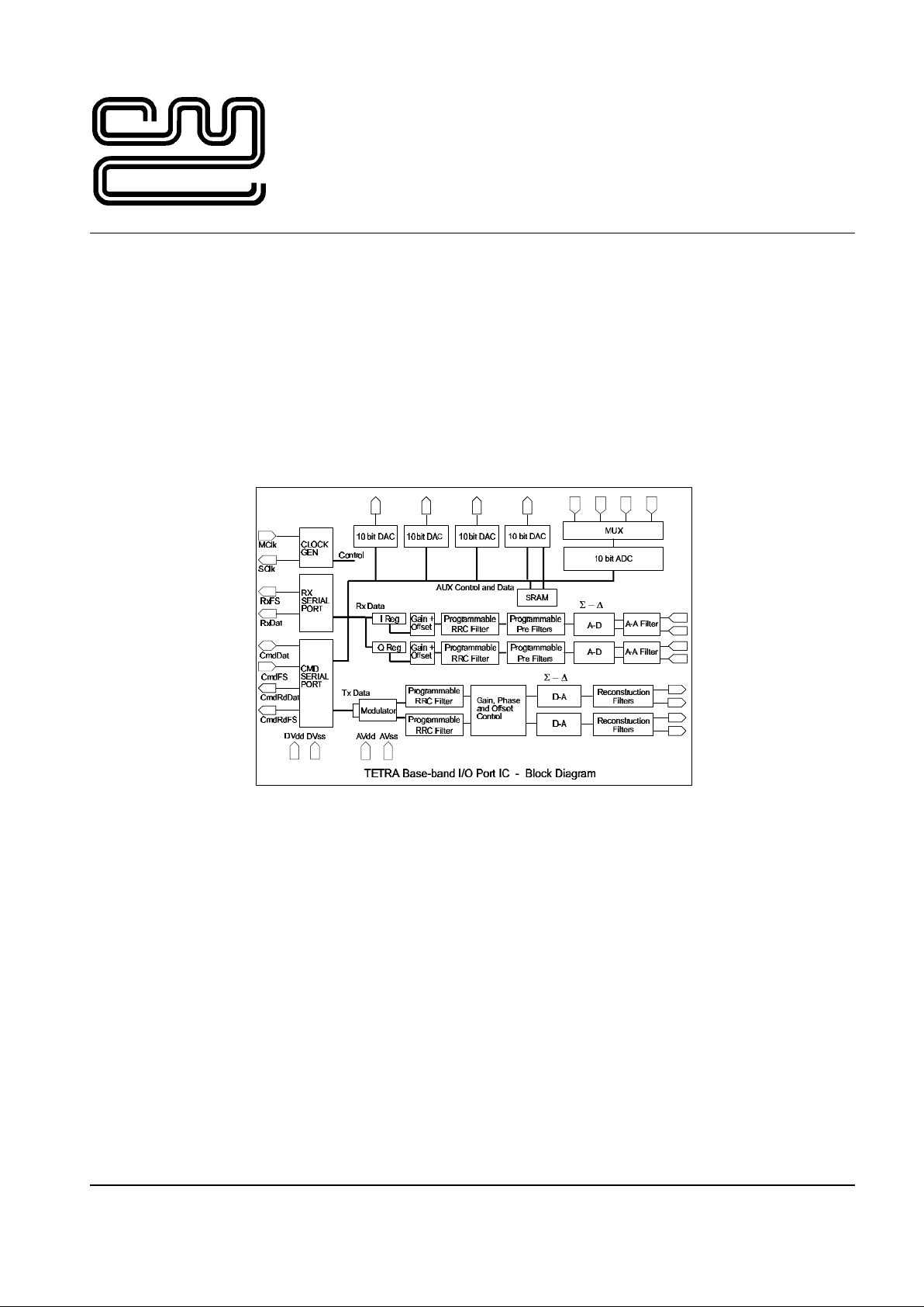
1.2 Block Diagram
Figure 1 Block Diagram
Page 4

TETRA Baseband Processor FX980
1997 Consumer Microcircuits Limited 4 D/980/3
1.3 Signal List
L6 Package
44 PLCC
Package
#
Signal Description
Pin No. Pin No. Name Type
15 MCLK I/P Master clock input (typically 9.216MHz)
16 SClk O/P Serial interface clock
17 CmdDat BI Command serial interface Data
18 CmdFS I/P Command serial interface Frame
19 CmdRdDat O/P Command serial interface Read Data
20 CmdRdFS O/P Command serial interface Read Frame
11 RxDat O/P Receive serial interface Data
12 RxFS O/P Receive serial interface Strobe
23 N_IRQ O/P Interrupt request
14 N_RESET I/P Chip Reset
24 SCANSEL I/P Scan Select (normally tied low)
25 ITXP O/P Transmit "I" channel, positive output
26 ITXN O/P Transmit "I" channel, negative output
30 QTXP O/P Transmit "Q" channel, positive output
29 QTXN O/P Transmit "Q" channel, negative output
42 IRXP I/P Receive "I" channel, positive input
41 IRXN I/P Receive "I" channel, negative input
38 QRXP I/P Receive "Q" channel, positive input
37 QRXN I/P Receive "Q" channel, negative input
43 AUXADC1 I/P Auxiliary ADC channel 1
44 AUXADC2 I/P Auxiliary ADC channel 2
1 AUXADC3 I/P Auxiliary ADC channel 3
2 AUXADC4 I/P Auxiliary ADC channel 4
Page 5

TETRA Baseband Processor FX980
1997 Consumer Microcircuits Limited 5 D/980/3
1.3 Signal List (continued)
L6 Package
44 PLCC
Package
#
Signal Description
Pin No. Pin No. Name Type
10 AUXDAC1 O/P Auxiliary DAC channel 1
9 AUXDAC2 O/P Auxiliary DAC channel 2
8 AUXDAC3 O/P Auxiliary DAC channel 3
7 AUXDAC4 O/P Auxiliary DAC channel 4
36 BIAS1 BI Analogue bias level. This pin should be de-
coupled to V
SSB.
35 BIAS2 BI Analogue bias level. This pin should be de-
coupled to V
SSB
.
32 V
CC1
Power I Channel analogue positive supply rail. This
pin should be de-coupled to V
SS1.
33 V
CC2
Power Q Channel analogue positive supply rail. This
pin should be de-coupled to V
SS2.
34 V
CC3
Power Analogue Bias positive supply rail. Levels and
voltages are dependent upon this supply. This
pin should be de-coupled to V
SSB.
6 V
DD1
Power Auxiliary analogue positive supply rail. This
pin should be de-coupled to V
SSA.
3,21 V
DD
Power Digital positive supply rail. This pin should be
de-coupled to V
SS.
27,40 V
SS1
Ground I Channel analogue negative supply rail.
28,39 V
SS2
Ground Q Channel analogue negative supply rail.
31 V
SSB
Ground Analogue Bias negative supply rail.
5 V
SSA
Ground Auxiliary analogue negative supply rail.
4,13,22 V
SS
Ground Primary digital negative supply rail.
Notes: I/P = Input
O/P = Output
BI = Bi-directional
Page 6
TETRA Baseband Processor FX980
1997 Consumer Microcircuits Limited 6 D/980/3
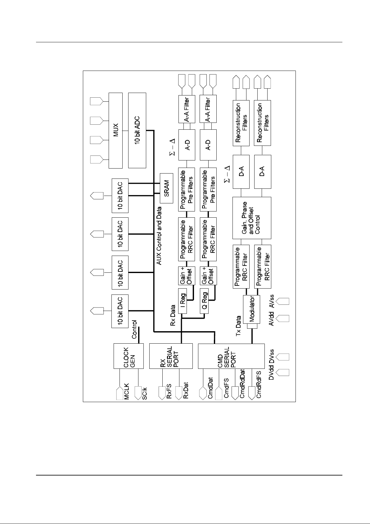
1.4 External Components
Rx Inputs
When using the internal anti-alias filter, the following is suggested
Example values:
R1 = 220
Ω C1 = 1.5nF (R1, C1 precise values are not critical) (-3dB at 240kHz)
R2 = 408
Ω C2 = 3.9nF (R2 x C2 time constant should be preserved) (-3dB at 50kHz)
When not using the internal anti alias filter, it is suggested that the user should follow the guidelines in Section
1.5.3.1. In both cases, there should be at least one filter pole close to the chip inputs.
Figure 2a Recommended External Components - Rx Inputs
Tx Outputs
Example values:
R3 = 220
Ω C3 = 1nF
Decoupling capacitors should be employed as detailed in Section 1.5.1
Figure 2b Recommended External Components - Tx Outputs
AGC
IRXP
IRXN
QRXP
QRXN
Filter 1
R2
R2
C2
R2
R2
C2
R1
R1
R3
R1
C1
C1
R1
C3
ITXP
ITXN
QTXP
QTXN
R3
C3
R3
R3
C3
C3
Page 7
TETRA Baseband Processor FX980
1997 Consumer Microcircuits Limited 7 D/980/3
1.5 General Description
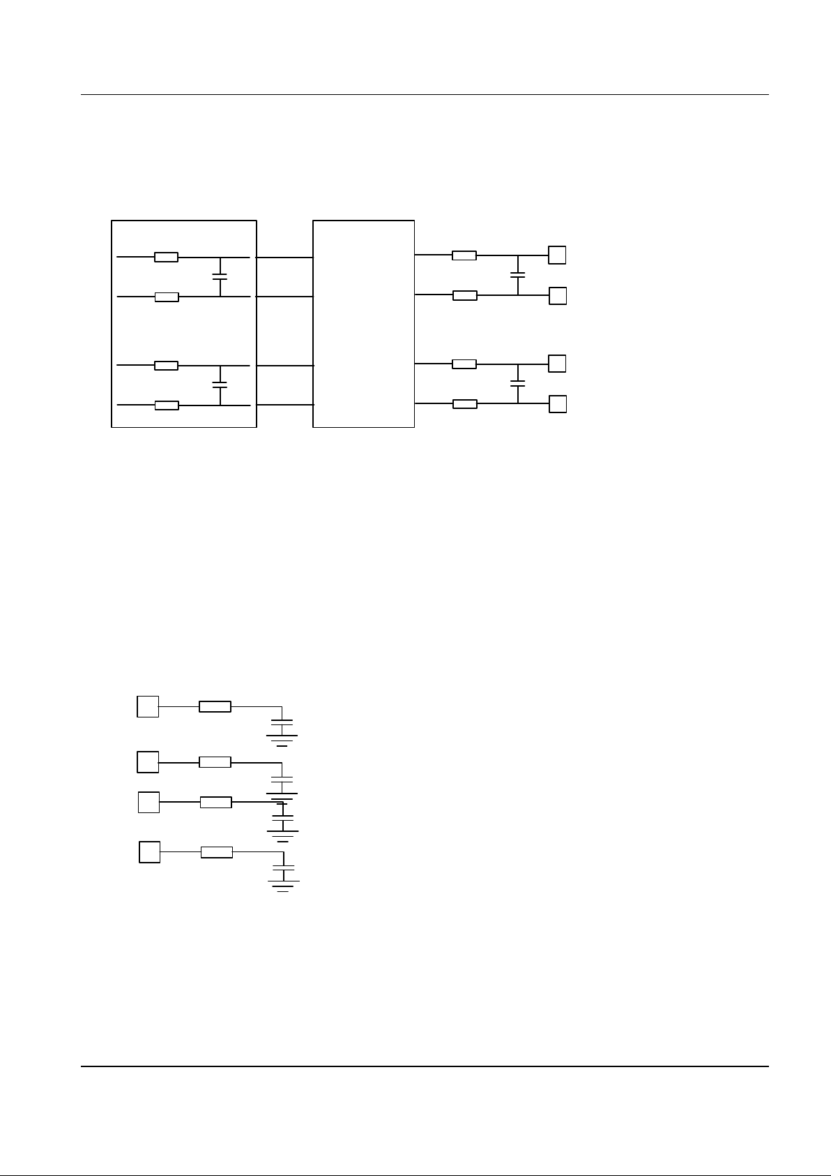
1.5.1 Connection and Decoupling of Power Supplies
Optimum performance from the FX980 can only be obtained by the use of adequate decoupling and
the separation of analogue and digital signals, including the use of separate ground planes.
Printed circuit board layout should follow the recommendations shown in Figure 3.
Figure 3 Recommended Decoupling Components
Page 8

TETRA Baseband Processor FX980
1997 Consumer Microcircuits Limited 8 D/980/3
1.5.2 Tx Data Path
The features described below give a high degree of flexibility for the user to compensate in the
baseband processing for non-ideal performance in the IF, RF and RF linear amplifier sections.
1.5.2.1 Modulator
This takes the 2-bit symbols, performs a Gray code conversion and uses a recursive adder to
generate a 3-bit code representing the 8 possible phase states. A look up table provides the digitally
encoded I and Q values for each phase state. The modulator function can be by-passed if required; in
this case the 3-bit code representing the 8 possible phase states which are passed to the look up
table is provided directly via the serial interface.
1.5.2.2 Filters
Digital filtering is applied to the data from the modulator; the coefficients are set as default to give a
Root Raised Cosine response with roll-off factor of 0.35. These FIR filters operate at 8x the incoming
symbol rate and are configured, for each channel, as two filters in cascade: the first filter has 79 taps
and the second filter has 49 taps. The first filter is used to enhance stop-band rejection and act as a
sampling correction filter and the second filter provides the primary shaping. Coefficients for the filters
may also be downloaded to the device via the serial interface; this gives the opportunity, if required, to
fine tune the frequency response of a complete system so as to minimise the BER or to use the
device in other applications. The filters can also be by-passed if required.
1.5.2.3 Gain Multiplier
This circuitry allows independent external control of the digital amplitudes in the I and Q channels to
12 bits of resolution. Extra circuits allow a mode of operation which will enable linear ramping up to a
maximum value, stay at this value for a specified duration, then ramp back down to zero. The
maximum value for each channel, the duration at maximum, the ramping up rate and the ramping
down rate are all programmable via the serial interface.
1.5.2.4 Offset Adjust
Offset registers allow any offsets introduced in the analogue sections of the transmit path to be
corrected digitally via the serial interface. The offset adjust has a resolution of 1 LSB and a maximum
value of 0.25x full scale.
1.5.2.5 Sigma-Delta D-A Converters and Reconstruction Filters
The converters are designed to have low distortion and >80dB dynamic range. These 3rd order
converters operate at a frequency of 128x symbol rate so as to over-sample the data at their inputs a
further 16 times. The reconstruction filters are 5th order, switched capacitor, low pass filters designed
to work in conjunction with an external RC.
1.5.2.6 Phase Pre-distortion
A further feature allows the user to compensate for a non-orthogonal carrier phase in the external
quadrature modulator by adding a programmable fraction of up to 1/8 of the filtered I and Q channel
signals to each other immediately prior to the DAC input.
1.5.2.7 Ramping Output Amplitude
A facility is provided to allow linear ramping of the outputs. This is accomplished, if enabled, by
multiplying the gain multiplier words by the ramping control register (RCR) value. The RCR is a 12-bit
word, representing a value from 0 to 1, which is designed to increment by an amount (INC) until its
maximum value. This value is held until a number of symbol times from the start of transmission
(TRD) when RCR decrements by an amount (DEC) until zero. INC, DEC and TRD are all 12-bit words
input via the serial interface prior to the start of a transmission.
Page 9

TETRA Baseband Processor FX980
1997 Consumer Microcircuits Limited 9 D/980/3
1.5.3 Rx Data Path
1.5.3.1 Anti-Alias Filtering and Sigma-Delta A-D Converters
The sampling frequency of the Sigma-Delta A-D is 128x symbol rate. The high oversampling rate
relaxes the design requirements on the anti-alias filter. However, to achieve optimum performance the
anti-alias filter must reject the sampling frequency to about -110dB, of which at least 40dB must be
provided externally. Additionally, in order to ease the complexity of the subsequent digital filters, there
is a further requirement that the anti-alias filter suppress 8x symbol rate to about -30dB. The on-chip
anti-alias filter is designed to achieve this when used in conjunction with some external filtering. If
required, the on-chip anti-alias filter can be by-passed and powered down, although external antialiasing must then be provided. The 4th order Sigma-Delta A-D converters are designed to have low
distortion and >96dB dynamic range. The baseband I and Q channels must be provided as differential
signals; this minimises in-band pick up both on and off the chip.
1.5.3.2 Filters
Digital filtering is applied to the data from the Sigma-Delta A-D converters; the default coefficients are
set to give a Root Raised Cosine response with roll-off factor of 0.35. These FIR filters are configured,
for each channel, as three filters in cascade. The first filter gives sufficient rejection at 8x symbol rate
to permit decimation at that frequency (note that -30dB is provided by the primary anti-alias filters).
The second filter has 63 taps and is used to enhance stop-band rejection. The third filter has 49 taps
and provides the primary shaping requirements. Coefficients for the second and third filters are
programmable via the serial interface. This gives the opportunity, if required, to fine tune the
frequency response of a complete system so as to minimise the BER or to use the device in other
applications. The filters can also be by-passed if required, by setting the centre coefficient to maximum
and all other coefficients to zero.
1.5.3.3 Offset Registers
System generated offsets may be removed by control of the offset register via the serial interface.
1.5.3.4 I and Q Channel Gain
Programmable gain modules are provided in both I and Q channels. These blocks allow the user to
adjust the dynamic range of the received data within the digital filters, thus optimising the filter signal
to noise performance for a range of levels at the Rx input pins.
The two channels are independently programmable. This enables differential gain corrections to be
made within the digital domain.
1.5.4 Auxiliary Circuits
1.5.4.1 10-Bit DACs
Four 10-bit DACs are provided to assist in a variety of control functions. The DACs are designed to
provide an output as a proportion of the supply voltage, depending on the digital input. They are
monotonic with an absolute accuracy of better than 1%. Control and Data for these come via the serial
interface.
1.5.4.2 10-Bit ADC
A 10-bit ADC is provided to assist in a variety of measurement and control functions. The ADC is
designed to produce a digital output proportional to the input voltage; full scale being the positive
supply. It is monotonic with an absolute accuracy of about 1%. An input multiplexer allows the input to
be selected from one of four sources. Control and digital data output is via the serial interface.
Page 10

TETRA Baseband Processor FX980
1997 Consumer Microcircuits Limited 10 D/980/3
1.5.4.3 Power Ramping and Control
One of the DACs has an additional feature which enables a set of values to be sequenced out at a
pre-selected frequency. This is aimed at enabling power ramping of a RF output with a suitable profile.
The sequence may be reversed for power down. The sequence of values is stored in a dedicated
RAM, which can be loaded via the serial interface.
1.5.5 IRQ Function
An interrupt request (IRQ) pin is provided for asynchronous communication with an external
processor. The IRQ (asserted low) will be asserted when any of the error or user information flags are
activated by an internal operation. Some examples of operations which may generate an IRQ are:
1. An attempt by the user to write to a full Tx data-input FIFO
2. An attempt is made by the Tx to read from the Tx data-input FIFO when it is empty.
3. An internal arithmetic overflow has occurred in an FIR filter.
The IRQ feature may also be used to establish the phasing of the received I and Q channel data from
the RxDat serial port should synchronisation be lost for any reason.
The cause of the IRQ can be obtained by reading the error flags register. All possible causes of an
IRQ are masked on reset. Mask status can be altered by writing to the IRQ mask register.
Note that default coefficients and settings have been optimised to maximise performance and should
not cause arithmetic overflows. However, use of non-default coefficients, large offset corrections or
large Tx phase adjustments may cause problems, which can be corrected by scaling down coefficients
or via the gain multiplier feature.
1.5.6 Serial Interface
All digital data I/O and control functions for the FX980 are via the serial interface. It is expected that
the FX980 will be used in conjunction with a DSP and/or other processor. The device has three serial
interface ports, each port is based on the industrial standard three wire serial interface. This interface
allows communication with standard DSP ICs using a minimum of external components. The three
serial interface ports are:
Cmd Command port, generally this is an input port receiving commands and data from the host,
but may also be configured as a bi-directional I/O interface.
CmdRd Command read port, an output port to send command read data back to the host. Read
data is only sent on this port in response to a read command.
RxData Receive data port, an output port to send receive data back to the host. Data is only
present on this interface when the Rx Data path is active. This port may also be
configured as the CmdRd port.
Page 11

TETRA Baseband Processor FX980
1997 Consumer Microcircuits Limited 11 D/980/3
Functions performed by the serial interface include:
• Power up or down and optional bypassing of selected blocks
• Setting digital filter coefficients
• Loading ramp up and ramp down increments and burst lengths for Tx
• Loading and transmitting data
• Loading offset correction, gain multiplier and phase adjustment registers
• Enabling/disabling of output via the Rx serial interface
• Vary sampling time for Rx data relative to the symbol (144kHz) clock.
• Loading data into auxiliary DACs
• Initiating conversions using auxiliary ADCs and reading results
• Writing data to, and reading data from, the Waveform Generation SRAM
• Power Ramping time step control
The three interfaces consist of the following signal pins:
SClk Output Serial Clock pin. This pin is common for all three interfaces.
CmdDat In/Out Command port Data pin. This pin is by default an input, but may be
configured as an open drain bi-directional pin.
CmdFS Input Command port Frame Sync pin. This pin is used to mark the first bit in a
serial frame.
CmdRdDat Output Command read port Data pin. This pin only has active data on it in
response to a read command.
CmdRdFS Output Command read port Frame Sync pin. This pin is used to mark the first bit in
a serial frame.
RxDat Output Receive data port Data pin. This pin is only active when the Rx Data path is
active.
RxFS Output Receive data port Frame Sync pin. This pin is used to mark the first bit in
a serial frame.
Note: All Frame Sync strobe signals are actually coincident with the last bit of a dataframe. See
Figures 4 and 5 for further details.
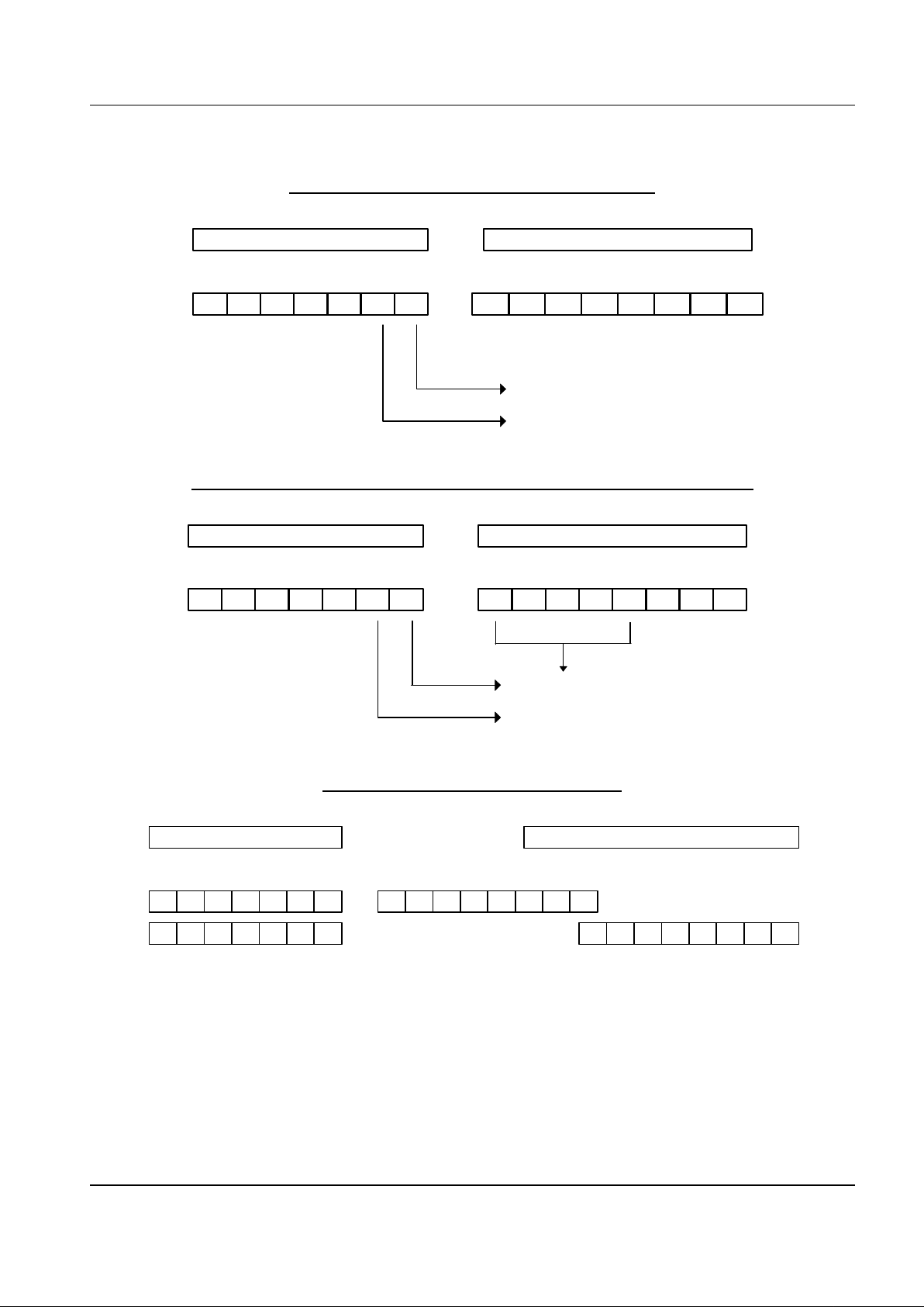
1.5.6.1 Command Interface
A serial command word consists of a 16-bit frame. Each frame is marked by an active Frame Sync
event which precedes the MSB bit. A command word can be either a control word or a transmit data
word.
MSB LSB
R/ W
Address Data
15 14 8 7 0
Command Control Serial Word
MSB LSB
1 Tx Data Address U/D 4/1 Tx Data
15 14 10 9 8 7 0
Command Transmit Data Serial Word
Page 12

TETRA Baseband Processor FX980
1997 Consumer Microcircuits Limited 12 D/980/3
1.5.6.2 Command Read Interface
Command read data is either output on one of the serial read ports, or driven out in the last 8 bits
(data field) on the Cmd port. When command read data is output on a serial read port, the read
address is put in the most significant half of the word, and the read data in the least significant half.
MSB LSB
0 Read Address Data
15 14 8 7 0
Command Read Serial Word
1.5.6.3 Rx Data Interface
The Rx Data interface is used only for output of the I and Q received data, unless it is operating in the
mode where CmdRd data is directed to it. When data reception is enabled, I and Q received data will
be output at either 8x or 4x the symbol rate, under control of command register RxSetup2. (see
Section 1.5.7). This is achieved by reducing the serial interface clock rate from MCLK/2 to MCLK/4
and discarding alternate data samples under control of command registers ConfigCtrl1 and
RxSetup2. 16-bit I and Q data words are output at the Rx Data interface, I data and MSB first (by
default), on the rising edge of SClk.
1.5.6.4 Transmission of Data
The address of the Tx FIFO is given consecutive locations ($0x04-$0x07), which allows the address
bits A1 and A0 (bits 11 and 10) of the Command Transmit Data Serial Word to be utilised as transmit
control functions. Data to be transmitted can be in either one or four (2-bit) symbol blocks, which are
subsequently modulated into the DQPSK constellation, or in 3-bit words, which map directly into
constellation points according to the table shown below.
3 bit
code
000 001 010 011 100 101 110 111
I
Q
1
0
0.7071
0.7071
0
1
-0.7071
0.7071
-1
0
-0.7071
-0.7071
0
-1
0.7071
-0.7071
Constellation map
The user initiates a transmit frame by asserting the TxEn bit in the TxSetup register. However,
internal transmission of the data will wait until specific conditions have been met. Firstly, a valid data
word must be written into the FIFO with the TxRampEn bit of the TxSetup register asserted.
Secondly, the internal symbol clock must be active. Therefore there is a variable delay between
asserting the TxEn bit and transmission starting. The user may poll the TxPathEn bit of the
TxFIFOStatus register to establish when transmission has started, and in this case the active state of
TxPathEn in High. In general, the user will wish to know when the transmit frame has completed.
This is indicated by TxPathEn returning Low.
To relieve the user of polling overheads when waiting for Tx frame completion, an interrupt can be set
up to occur on the transition of the TxPathEn bit from High to Low. In such circumstances, the
interrupt activation state of the TxPathEn can be considered Low.
Page 13

TETRA Baseband Processor FX980
1997 Consumer Microcircuits Limited 13 D/980/3
Two control bits are associated with each data transmission word. One controls the format of the word
and the other initiates and terminates a transmission cycle. This close association enables precise
control of the transmission frame. To relieve the user of the need to synchronise each TxData write
with the internal transmit cycle, transmit data words are written into an internal 4-word-deep FIFO.
Symbols or constellation points are then read as needed from this FIFO. It is necessary to make sure
that there is always a word to be read, and also that the FIFO is never written to when full. This may
be accomplished by using one of two data interlock mechanisms.
Data Interlock Mechanisms
There are two possible transmission data interlock mechanisms. It is recommended that the user
should always use one of these methods.
• Software polling.
• Serial Clock when ready.
Software polling requires the user to first check that the FIFO is not full before writing each TxData
word. This may be accomplished by inspecting the relevant FIFO status bits before writing one or
more TxData words.
The Serial Clock when ready method is a hardware interlock mechanism (enabled by setting the
TxHandshakeEn bit of ConfigCtrl1 register active). The mechanism allows the user to write TxData
words without doing any FIFO checks: the hardware handshake is implemented by stopping the serial
port clock when the FIFO is full. To prevent a serial port lockout-condition, the handshake is only
enabled once the transmission frame has been initiated and is automatically disabled at the end of a
frame. This mechanism should be used with care, because stopping the clock will freeze all other
serial port transfers (the serial port clock SClk is common to all three serial ports), including access to
auxiliary data converters and receive data.
Power Ramping and Frame Interlock
The RampUp bit in the TxData word is used to control both the power ramping function and the frame
activation. To start a transmission frame, a transmission word is written with the RampUp bit active. All
subsequent TxData words prior to frame termination must also have this bit active. The frame is
terminated by writing transmit data words with the RampUp bit inactive. Subsequent TxData words
must also have this bit inactive, until initiation of a new frame is required. While the power ramping is
active (up or down) the user must supply transmission symbols or valid constellation points. Once the
ramp down operation has completed, all subsequent TxData writes with the RampUp bit inactive will
be ignored.
1.5.6.5 Command Control Serial Word
A command word either directly accesses an internal register for a read or write operation, or
addresses a memory access point to indirectly access a block of internal memory. For test purposes
all registers that can be written may also be read. Not all registers may be written, as some are just
status registers. Each register or memory access point is assigned a unique address: the whole (8bit) address range is reserved for the FX980.
Indirect Memory Addressing
All internal memory access is via an access point. First, a command word access is used to reset the
internal address pointer, then data port access operations post-increment this address pointer.
Page 14

TETRA Baseband Processor FX980
1997 Consumer Microcircuits Limited 14 D/980/3
Example: To program the fifth and sixth locations of the Auxiliary SRAM with $0x01AA the
commands would be:
$0x0000
⇒Cmd
; set ConfigCtrl1 all bits Low ; use default conditions
$0x0118
⇒Cmd
; set ConfigCtrl2 bits 7 and 6 Low ; required by default for these
Reserved bits
; set ConfigCtrl2 bit 4 High ; post-increment addresses on a
read operation
; set ConfigCtrl2 bit 3 High ; enable read/write access to the
Auxiliary SRAM
$0xF300
⇒Cmd
; read SramData LSB register ; read fourth memory location
(LSB). Post-increment pointer.
CmdRd
⇒$0xF3xx
; SramData LSB register data returned ; discard this byte
$0x7002
⇒Cmd
; write SramData LSB register ; write $0x02 to fifth memory
location (LSB)
$0x716A
⇒Cmd
; write SramData MSB register ; write $0x6A to sixth memory
location (MSB)
$0xF000
⇒Cmd
; read SramData LSB register ; read fifth memory location (LSB)
CmdRd
⇒$0xF002
; SramData LSB register data returned ; check this byte is $0x02
$0xF100
⇒Cmd
; read SramData MSB register ; read sixth memory location (MSB)
CmdRd
⇒$0xF16A
; SramData MSB register data returned ; check this byte is $0x6A
$0x0110
⇒Cmd
; set ConfigCtrl2 bit 3 Low ; disable read/write access to the
Auxiliary SRAM
1.5.6.6 Coefficient Memory
The convention for naming filter coefficients is A1 to An, where n is given by (Filter Length + 1)/2, i.e. for the
15-tap filter, n = 8. This arises from the internal architecture of the filters and the fact that they are all “odd”
and symmetrical. Write or read operations beyond this coefficient number will be reflected about the central
coefficient e.g. the tenth read operation from the 15-tap filter would access coefficient location A6.
There is no practical reason to write or read beyond location n, but the user in any case must avoid write
operations at the (Filter Length + 1) location. This location (A0) location must be zero for the filters to operate
correctly. The global reset (N-RESET pin) establishes this condition when taken Low.
1.5.7 Register Description
This section describes in detail each of the registers and access points addressed by the Command Control
Serial Word.
Page 15

TETRA Baseband Processor FX980
1997 Consumer Microcircuits Limited 15 D/980/3
Key to Register Map
Each section that follows describes in detail the operation and use of each of the registers in the device. The
registers are split into their functional groups, grouping associated registers together. Each section consists of
a Title, an Address, a Function Reference Field, a Description, and a Bit Specification.
The Function Reference Field describes the overall access available to this section (RW/W/R, where R = Read
and W = Write).
The Bit Specification describes the function of each individual bit, or a range of bits within a register. There is a
separate line for each distinct field of bits. The State column indicates the action available to each group of
bits (RW/W/R).
Register Reset State
All I/O access points (both read and write) are reset to logic zero on taking N_RESET Low, except where
explicitly shown in this document. The reset state of status bits will depend on the level of the status signal
being monitored. Other registers (both read and write) are not affected by taking N_RESET Low.
Page 16

TETRA Baseband Processor FX980
1997 Consumer Microcircuits Limited 16 D/980/3
1.5.7.1 Register and Access Point Summary
Control and Status Registers
$0x00
ConfigCtrl1
Configuration control register 1
$0x01
ConfigCtrl2
Configuration control register 2
$0x02
PowerDownCtrl
Power control register
$0x03
TxSetup
Transmit set-up register
$0x04-$0x07
TxData
Transmit data registers
$0x08
RxSetup1
Receive set-up control register 1
$0x09
RxSetup2
Receive set-up control register 2
$0x0A
AnaCtrl
Analogue configuration control register
$0x0B
AuxAdcCtrl
Auxiliary ADC data converter control register
$0x0C
RamDacCtrl
Ram Dac control register
$0x0D
LoopBackCtrl
Loopback control register
$0x0E
TxErrorStatus
Transmit error status register
$0x0F
TxErrStatMask
Transmit error status interrupt mask register
Auxiliary Function Registers
$0x10-$0x17
AuxAdcData
Auxiliary ADC data registers
$0x18-$0x1F
AuxDacData
Auxiliary DAC data registers
Status and Interrupt Registers
$0x20
RxErrorStatus
Receive error status register
$0x21
RxErrorStatMask
Receive error status interrupt mask register
$0x22
TxFIFOStatus
Transmission data FIFO status register
$0x23
TxFIFOStatMask
Tx data FIFO status interrupt mask register
Memory I/O Access Points
$0x24-$0x2D
CoeffRamData
Coefficient memory I/O access addresses
$0x2E-$0x2F Not Used.
Rx Data Path Registers
$0x30-$0x31
RxIQGainMult
Receive I channel gain attenuation registers
$0x32-$0x33
RxIQOffset
Receive I channel offset correction registers
$0x34-$0x35
RxIQGainMult
Receive Q channel gain attenuation registers
$0x36-$0x37
RxIQOffset
Receive Q channel offset correction registers
Page 17

TETRA Baseband Processor FX980
1997 Consumer Microcircuits Limited 17 D/980/3
Rx Data Path Access Points
$0x38-$0x39
RxDataAccess
Receive path data access point (I)
$0x3A-$0x3B
RxDataAccess
Receive path data access point (Q)
$0x3C-$0x3F Not Used
Tx Data Path Registers
$0x40-$0x41
TxPhase
Transmit I channel phase correction registers
$0x42-$0x43
TxIQGainMult
Transmit I channel gain attenuation registers
$0x44-$0x45
TxIQOffset
Transmit I channel offset correction registers
$0x46-$0x47
TxPhase
Transmit Q channel phase correction registers
$0x48-$0x49
TxIQGainMult
Transmit Q channel gain attenuation registers
$0x4A-$0x4B
TxIQOffset
Transmit Q channel offset correction registers
$0x4C-$0x4D
TxRampUpInc
Transmit ramp-up increment registers
$0x4E-$0x4F
TxRampDnDec
Transmit ramp-down decrement registers
Tx Data Path Access Points
$0x50-$0x51
TxDataAccess
Transmit path data access point (I)
$0x52-$0x53
TxDataAccess
Transmit path data access point (Q)
$0x54-$0x5F Not Used
Self Test Registers
$0x60-$0x61
BISTPRSG
Built-in self test pseudo-random sequence generator
$0x62
BISTControl
Built-in self test control register
$0x63 Not Used
$0x64-$0x6D
BISTCRCRegisters
Built-in self test cyclic redundancy code checkers
$0x6E-$0x6F Not Used
SRAM Memory Access Points
$0x70-$0x73
SramData
Auxiliary DAC1 memory I/O access addresses
$0x74-$0x7F Not Used
Note: Addresses $0x80 to $0xFF cannot be used as the MSB controls the direction of data flow:
“1” = High = Read and “0” = Low = Write.
Page 18

TETRA Baseband Processor FX980
1997 Consumer Microcircuits Limited 18 D/980/3
ConfigCtrl1
Title: Configuration Control register
Address: $0x00
Function: RW
Description: General configuration bits, together with operational control signal bits.
Bit Name Active State Function
7 DataRateHi High RW When set active all serial port data transfers will be at
half of the master clock rate. When inactive, all serial
port data rates will be at a quarter of the master clock
rate. This has the effect of altering the Rx sample output
rate from 8 times the symbol rate when active to 4 times
when inactive.
6 TxHandshakeEn High RW When set active enable the transmit hardware interlock
protocol, thereby stopping the Serial Clock (SClk) if the
transmit path is enabled and the transmit FIFO is full.
5 BiDirCmdPortEn High RW When this bit is set active the Cmd port will drive its
data line out of the chip for the last 8 bits of read
operations. When set inactive command read data will
be returned on either the Rx or the CmdRd port
(default).
4 RxDataForCmdRdEn High RW This bit only takes effect if the BiDirCmdPortEn bit is
inactive. When set active this bit causes all command
read operations to respond with data on the Rx serial
port. When set inactive the command read data will be
output via the CmdRd port (default).
(5,4) CommandReadDataMode RW The BiDirCmdPortEn bit and RxDataForCmdRdEn bit
together control the method by which command read
data is returned to the user.
00 (Default) Read data returned on CmdRd port.
01 Read data returned on Rx port and CmdRd port
10,11 Read data returned on Cmd port.
3 LowRxRdFS High RW When set active both the CmdRdFS and the RxFS
output pins will be driven active low, when set inactive
the two frame sync's will be driven active high (default).
2 RxDataPortDisable High RW When set active tristates the RxDat and RxFS pins.
1 RdCmdPortDisable High RW When set active tristates the CmdRdDat and CmdRdFS
pins.
0 SymboModuBypass High RW Setting this bit bypasses the Modulator, thereby taking
the least significant 3 bits of each Command Transmit
Data Serial Word received via the serial interface to
represent an absolute constellation mapping.
Page 19

TETRA Baseband Processor FX980
1997 Consumer Microcircuits Limited 19 D/980/3
• Address and Data format for ConFigCtrl1 access
Data field [7:0]
D7 D6 D5 D4 D3 D2 D1 D00000 0 0 0
Address field [6:0]
Page 20

TETRA Baseband Processor FX980
1997 Consumer Microcircuits Limited 20 D/980/3
ConfigCtrl2
Title: Configuration Control register
Address: $0x01
Function: RW
Description: General configuration bits, together with operational control signal bits.
Bit Name Active State Function
7 RW Reserved. Set this bit Low. Undefined on read.
6 RW User defined bit. This bit has no internal functionality and
is reset Low with the global N_RESET pin. The user may
employ this bit for any useful purpose.
5 n_SlowDown Low RW When active, this bit reduces the slew rate of digital output
pins. This reduces power consumption, ground bounce and
reflection problems associated with fast edges on poorly
terminated lines. De-activation speeds up the digital
outputs, but increases power consumption, ground bounce
and reflection problems. It is anticipated that the latter
mode will be used only in 3.3V systems.
4 SRamIoRdInc High RW This bit determines whether a read or write operation to the
Auxiliary SRAM will increment the address pointers. When
set active causes read operations to move the address
pointer on, this would therefore allow an efficient write then
read verify scheme to be used. When set inactive write
operations increment the address pointer.
3 SRamloEn High RW When set active allows read/write access to the Auxiliary
SRAM. It is only valid to activate this bit when the SRAM is
not being accessed by the RamDac. When this bit is set
active, the first access to SramData will access the first
SRAM address location. Subsequent read or write
accesses will increment the address pointer to the next
memory location.
2 CoeffRamIoRdInc High RW This bit determines whether a read or write operation to a
coefficient memory will increment the address pointers.
When set active the address pointer is incremented by any
coefficient ram read operation, thereby allowing a write
then read verification. When set inactive, write operations
increment the address pointer.
1 CoeffRamloEn High RW When set active allows read/write access to all the
coefficient memories. This bit is valid only when the Tx and
Rx Data paths are inactive. When this bit is set active, the
first access to any of the coefficient memories will access
the first coefficient location (A1). Subsequent read or write
accesses to any coefficient memory will increment the
address pointers for all the coefficient memories.
Page 21

TETRA Baseband Processor FX980
1997 Consumer Microcircuits Limited 21 D/980/3
0 n_BigEndData Low RW When set active causes serial port read data, from the Rx
port to be generated with the MSB data bit as the first serial
word bit. If inactive, the LSB is first. On taking N_RESET
Low this bit is active (i.e. the default is MSB first).
• Address and Data format for ConFigCtrl2 access
Data field [7:0]
R D6 D5 D4 D3 D2 D1 D01000 0 0 0
Address field [6:0]
Page 22

TETRA Baseband Processor FX980
1997 Consumer Microcircuits Limited 22 D/980/3
PowerDownCtrl
Title: Power Control register
Address: $0x02
Function: RW
Description: This register, together with the following bits, controls the power saving features:
TxEn bit of register TxSetup
RxEn bit of register RxSetup1
TxClkStop bit of register TxSetup
RxClkStop bit of register RxSetup1
Bit Name Active State Function
7 RW Reserved. Set this bit Low. Undefined on read.
6 BiaslCtrl High RW When set active, increases Tx and Rx analogue bias
currents.
5 BiasPowDn Low RW When set active powers down the analogue bias section.
4 AuxDac4PowDn Low RW When set active powers down Auxiliary Dac4.
3 AuxDac3PowDn Low RW When set active powers down Auxiliary Dac3.
2 AuxDac2PowDn Low RW When set active powers down Auxiliary Dac2.
1 AuxDac1PowDn Low RW When set active powers down Auxiliary Dac1.
0 RxAafPowDn Low RW When set active powers down the receive analogue
anti-alias filter (AAF).
• Address and Data format for PowerDownCtrl access
Data field [7:0]
R D6 D5 D4 D3 D2 D1 D00100 0 0 0
Address field [6:0]
Page 23

TETRA Baseband Processor FX980
1997 Consumer Microcircuits Limited 23 D/980/3
TxSetup
Title: Transmit Set-up register
Address: $0x03
Function: RW
Description: Sets up the transmit functions.
Bit Name Active State Function
7:4 RW Reserved. Set these bits Low. Undefined on read.
3 TxClkStop High RW When set active causes the TxEn bit to also be used to
gate the Tx Data path master clock. When inactive (default
state) the Tx Data path master clock is always supplied.
2 TxEn High RW When set active, enables the Tx Data path, allowing
transmission to start when the correct enable sequence
has been seen. This bit may only be cleared when the
TxPathEn status bit in the TxFIFOStatus register is
inactive, setting inactive during a transmission cycle will
cause erroneous behaviour. This bit also acts as a transmit
section power enable bit.
1 TxRampEn High RW When set active, this bit enables the transmit amplitude
ramping function. Ramping is then controlled by the
TxRampUp bit of the TxData register When this bit is
inactive, the TxRampUp bit will directly control the transmit
amplitude (High meaning full amplitude, Low meaning zero
amplitude).
0 TxFirCoeffReset Low RW When set active this bit forces all the Tx Data path filters to
load their default coefficient values. This bit will be set
active on taking N_RESET Low, and therefore needs to be
deactivated before default filter coefficients can be
overwritten.
• Address and Data format for TxSetup access
Data field [7:0]
R R R R D3 D2 D1 D01100 0 0 0
Address field [6:0]
Page 24

TETRA Baseband Processor FX980
1997 Consumer Microcircuits Limited 24 D/980/3
TxData
Title: Transmit Data register
Address: $0x04 - $0x07 (Mapped over four locations, two address bits being used as data bits)
Function: W FIFO input
R FIFO output
Description: This transmit data register is 10 bits wide. The two least significant bits of the address bus are
used to drive bits 8 and 9, hence it can be considered to be mapped over four consecutive
locations. This data word is written into a FIFO. The function is only decoded when the FIFO is
read (there is an exception for the first data word). The FIFO will be read when the Tx Data path
demands data. This will only occur when the TxEn bit of the TxSetup register is set active. For
test purposes the FIFO data output may be accessed by reading these registers.
Data write with symbol modulator not bypassed
Bit Name Active State Function
9 TxRampUp High W This bit is written to the FIFO. While the TxEn bit of the
TxSetup register is active, it controls the Tx Data path
ramping. Setting it active will cause the amplitude to ramp
up to its full value, conversely setting the bit inactive will
cause the amplitude to ramp down to its minimum value. If
the bit is changed while the amplitude is being ramped, the
ramp direction will change to the direction set by this bit.
While the TxRampEn bit is inactive, the TxRampUp bit will
directly control the transmit amplitude (High meaning full
amplitude and Low meaning zero amplitude).
8 MultiSymbol High W This bit is written to the FIFO and when this bit is set
active, the FIFO symbol data will be marked as a four
symbol word. When set inactive, the FIFO symbol data
will be marked as a single symbol word. This bit is inactive
if the SymbModuBypass bit of the ConfigCtrl1 register is
active.
7:6 TxRelSymbol4 Data W Fourth symbol in word to be written to FIFO.
5:4 TxRelSymbol3 Data W Third symbol in word to be written to FIFO.
3:2 TxRelSymbol2 Data W Second symbol in word to be written to FIFO.
1:0 TxRelSymbol1 Data W First symbol in word to be written to FIFO.
Data write with symbol modulator bypassed
Bit Name Active State Function
9 TxRampUp High W (See above)
8:3 (not used) Data W Redundant data which is still written into the FIFO. Set
these bits Low.
2:0 TxAbsSymbol Data W IQ constellation point which is written into the FIFO.
Page 25

TETRA Baseband Processor FX980
1997 Consumer Microcircuits Limited 25 D/980/3
Read operation
Bit Name Active State Function
Address $0x04
7:2 Reserved. Bit values are not defined.
1:0 UpperFIFORdData Data R Reads address access bits 9 and 8 of the FIFO data output
register, these are placed in bits 1 and 0.
Address $0x05
7:0 LowerFIFORdData Data R Reads address access bits 7 to 0 of the FIFO data output
register. Reading this location also performs a FIFO read
operation, thereby moving the next (if any) FIFO data
location into the FIFO data output register.
Address $0x06 and $0x07
7:0 R Reserved. Bit values are not defined.
For these read operations to be valid, the Tx Data path must be active (TxEn bit of TxSetup register set
active) and the SymbModuBypass bit of the ConfigCtrl1 register must also be set active.
Page 26
TETRA Baseband Processor FX980
1997 Consumer Microcircuits Limited 26 D/980/3
Address and Data format for TxData Write access
D8
Data field [7:0]
D910000Address field [6:0]
D1D0D7D6D5D4D3
D2
MultiSymbol bit
TxRampUp bit
Address and Data format for TxData (Modulator Bypass Mode) Write access
NU
Data field [7:0]
D910 0 0 0
Address field [6:0]
D1 D0NU NU NU NU NU D2
Not Used
TxRampUp bit
Address and Data format for TxData Read access
Data field [7:0]
0010 0 0 0
Address field [6:0]
D9 D8R R R R R R
D1 D0D7 D6 D5 D4 D3 D21010 0 0 0
Page 27

TETRA Baseband Processor FX980
1997 Consumer Microcircuits Limited 27 D/980/3
RxSetup1
Title: First Receive Set-up control register
Address: $0x08
Function: RW
Description: Receive path set-up and initialisation control bits.
Bit Name Active State Function
7 Rx32BitMode High RW When set active, the Rx port operates on 32-bit frames -
I data in the MSB word, Q data in the LSB word.
6 RxSampleSel High RW This bit is used to select which pair of I,Q samples is
supplied from the possible two when the DataRateHi bit in
ConfigCtrl1 register is in the low mode (inactive). It has no
effect when DataRateHi is active.
5 RxClkStop High RW When set active causes the RxEn bit to also be used to
gate the Rx Data path master clock. When inactive (default
state) the Rx Data path master clock is always supplied.
4 RxEn High RW When set active, enables the Rx Data path, which then
starts to process the differential data on the IRXP,IRXN
and QRXP,QRXN pins, outputting results via the Rx serial
port. This bit also acts as a receive section power enable
bit.
3 RxBistActive High RW When set active, enables Rx Built-In Self Test (BIST)
operation.
2 AnaAdcReset Pulse W When this bit is set High, a 4-clock-cycle ADC auto reset
event is generated. It is not necessary to clear this bit
before another ADC auto reset event is initiated.
R The read state of this bit indicates the logic level last written
to this bit. It does not have a functional significance and is
only available for test purposes.
1 AnaEnAutoReset Low RW When active this bit enables the ADC auto reset function.
On taking N_RESET Low, this bit is set active, which is the
default operating condition.
0 RxFirCoeffReset Low RW When set active forces all the Rx Data path filters to load
their default coefficient values. This bit will be set active on
taking N_RESET Low, and therefore needs to be
deactivated before default filter coefficients can be
overwritten. Normal filter operation is unaffected by leaving
this bit set.
Page 28

TETRA Baseband Processor FX980
1997 Consumer Microcircuits Limited 28 D/980/3
• Address and Data format for RxSetup1 access
Data field [7:0]
D7 D6 D5 D4 D3 D2 D1 D00000 0 0 1
Address field [6:0]
Page 29

TETRA Baseband Processor FX980
1997 Consumer Microcircuits Limited 29 D/980/3
RxSetup2
Title: Second Receive Set-up control register
Address: $0x09
Function: RW
Description: Receive I and Q vernier control bits.
Bit Name Active State Function
7:4 QvernierDelay High RW Q channel Vernier sampling delay, allowing the sampling
point to be adjusted to a resolution of 1/16 of the input
sample clock rate.
3:0 IvernierDelay High RW I channel Vernier sampling delay, allowing the sampling
point to be adjusted to a resolution of 1/16 of the input
sample clock rate.
Note: The values are in the format of 4 bit signed 2s-complement integers - the MSB being the sign. Thus it
can be interpreted as adjusting the reference phase by ± 7/16 of the sample clock period.
• Address and Data format for RxSetup2 access
Data field [7:0]
D7 D6 D5 D4 D3 D2 D1 D01000 0 0 1
Address field [6:0]
Page 30

TETRA Baseband Processor FX980
1997 Consumer Microcircuits Limited 30 D/980/3
AnaCtrl
Title: Analogue configuration Control register
Address: $0x0A
Function: RW
Description: Reserved. All bits should be set Low.
Page 31

TETRA Baseband Processor FX980
1997 Consumer Microcircuits Limited 31 D/980/3
AuxAdcCtrl
Title: Auxiliary ADC data converter Control register
Address: $0x0B
Function: RW
Description: This register controls the operation of the four ADC channels. These are implemented using a
single ADC converter which is multiplexed on to each of the ADC channels. A conversion cycle
consists of performing a conversion for each of the active channels in turn.
Bit Name Active State Function
7 RW Reserved. Set this bit Low. Undefined on read.
6 AdcConvertRate High RW This bit changes the ADC conversion rate. If this bit is set
Low, the ADC is clocked by MCLK/8, yielding a conversion
time of 80x MCLK periods per ADC channel. The maximum
sample rate is lower than this. With a single channel
selected, the maximum rate is MCLK/112 samples/second.
Setting this bit high will halve the ADC clock rate, and hence
double the conversion time.
5 AdcContConv High RW Continuous conversion mode control bit; when inactive, sets
the ADCs into one-shot conversion mode; when active, the
ADCs will continuously convert. One-shot conversion mode
is initiated by the StartConvert bit. In continuous convert
mode, the ADC will start a new conversion cycle on all active
channels after the previous cycle has completed.
4 EnableAdc4 High RW Setting this bit high will enable ADC channel 4 for
conversion. This bit may be updated at any time, but will
only change the active state of the ADC channel for the next
time it is converted.
3 EnableAdc3 High RW Setting this bit high will enable ADC channel 3 for
conversion. This bit may be updated at any time, but will
only change the active state of the ADC channel for the next
time it is converted.
2 EnableAdc2 High RW Setting this bit high will enable ADC channel 2 for
conversion. This bit may be updated at any time, but will
only change the active state of the ADC channel for the next
time it is converted.
1 EnableAdc1 High RW Setting this bit high will enable ADC channel 1 for
conversion. This bit may be updated at any time, but will
only change the active state of the ADC channel for the next
time it is converted.
Page 32

TETRA Baseband Processor FX980
1997 Consumer Microcircuits Limited 32 D/980/3
0 StartConvert High One-shot conversion control bit. Only valid when the ADCs
are set to one-shot conversion mode.
W Setting this bit High starts the ADC data conversion. Setting
this bit Low will stop the conversion. This should only be
used for test purposes, because the ADC conversion logic
will automatically set this bit Low when the conversion
operation has completed.
R This bit can be set High or Low by the serial interface, but
the ADC conversion logic will automatically set it Low when
the current conversion cycle has completed.
• Address and Data format for Auxillary ADC Control access
Data field [7:0]
R D6 D5 D4 D3 D2 D1 D01100 0 0 1
Address field [6:0]
Page 33

TETRA Baseband Processor FX980
1997 Consumer Microcircuits Limited 33 D/980/3
AuxAdcData
Title: Auxiliary ADC Data registers
Address: (Eight registers) $0x10 to $0x17
Function: R
Description: These registers enable the user to inspect the conversion value for each of the four auxiliary
ADCs. There are two read registers per ADC, one to obtain the least significant two bits of the
data, the other for the most significant eight bits. Reading these registers does not affect the
ADC conversion cycle. Reading the MSB read register directly reads the ADC output and
simultaneously causes the two bits in the LSB read register to be written into a holding register.
This holding register is read when the LSB read register is read. This mechanism is necessary
to allow the user to read MSB and LSB data from the same ADC conversion cycle. If only the
MSB read register is read, the converter can be considered as an 8-bit ADC. If a 10-bit
conversion is required, the MSB read register must be read first.
Bit Name Active State Function
Address $0x10
7:0 Adc1MsbData Data R Most significant eight bits of the data from the last
conversion of AuxAdc1.
Address $0x11
7:2 R Reserved. Bit values are not defined.
1:0 Adc1LsbData Data R Least significant two bits of the data from the last
conversion of AuxAdc1.
Address $0x12
7:0 Adc2MsbData Data R Most significant eight bits of the data from the last
conversion of AuxAdc2.
Address $0x13
7:2 R Reserved. Bit values are not defined.
1:0 Adc2LsbData Data R Least significant two bits of the data from the last
conversion of AuxAdc2.
Address $0x14
7:0 Adc3MsbData Data R Most significant eight bits of the data from the last
conversion of AuxAdc3.
Address $0x15
7:2 R Reserved. Bit values are not defined.
1:0 Adc3LsbData Data R Least significant two bits of the data from the last
conversion of AuxAdc3.
Address $0x16
7:0 Adc4MsbData Data R Most significant eight bits of the data from the last
conversion of AuxAdc4.
Address $0x17
7:2 R Reserved. Bit values are not defined.
1:0 Adc4LsbData Data R Least significant two bits of the data from the last
conversion of AuxAdc4.
Page 34

TETRA Baseband Processor FX980
1997 Consumer Microcircuits Limited 34 D/980/3
Address and Data format for Auxillary ADC Data access
0
1
Data field [9:0]
D9 D8 D7 D6 D5 D4 D3 D2
R R R R R R D1 D0N0N10 0 1 0
N0N10 0 1 0
N1 N0 ADC Channel
0 0 Channel 1
0 1 Channel 2
1 0 Channel 3
1 1 Channel 4
Address field [6:0]
Page 35

TETRA Baseband Processor FX980
1997 Consumer Microcircuits Limited 35 D/980/3
RamDacCtrl
Title: RamDac Control register
Address: $0x0C
Function: RW
Description: This register controls the operation of DAC 1, together with the operation of the memory
(DacSram) which can be used to drive the digital input of DAC 1.
Bit Name Active State Function
7:6 RW Reserved. These bits should be set Low. Undefined on
read.
5:3 RamDacRate High RW These three bits set the rate at which the RamDac
memory’s DAC access address pointer changes. The three
bit value (RamDacRate) causes a change rate of
(36 x
2
RamDacRate
) kHz. See table below.
2 RamDacInc High RW This bit activates the RamDac memory scan operation.
Setting it active will cause the memory address to
increment up to the top (highest) location, conversely
setting the bit inactive will cause the memory address to
decrement down to the bottom location. If the bit is
changed while the memory is being scanned, the current
scan will complete before the new state of the RamDacInc
bit takes effect.
1 AutoCycle High RW This bit is only valid if the RamDacActive bit is active.
When set active, the Auxiliary SRAM memory will be
continually scanned at the rate set by the RamDacRate
bits. This enables a symmetrical periodic waveform to be
driven out on the AUXDAC1 pin. The Auxiliary SRAM
address cycles from the bottom location up to the top
location, and back down to the bottom again.
0 RamDacActive High RW DAC 1 input mode bit. When inactive, the AuxDacData
registers (offsets 0 and 1) are used as the source for
conversion. If this bit is active, the DAC is driven from the
output of the RamDac memory.
Ram Dac Rate Select Table
RamDacCtrl[5:3] Dac Update Frequency
(kHz)
0 0 0 36
0 0 1 72
0 1 0 144
0 1 1 288
1 0 0 576
1 0 1 1152
1 1 0 2304
1 1 1 4608
Page 36

TETRA Baseband Processor FX980
1997 Consumer Microcircuits Limited 36 D/980/3
• Address and Data format for RamDacCtrl access
D1 D0R R D5 D4 D3 D2
Data field [7:0]
Address field [6:0]
0 00 0 0 1 1
Page 37

TETRA Baseband Processor FX980
1997 Consumer Microcircuits Limited 37 D/980/3
AuxDacData
Title: Auxiliary DAC Data registers
Address: (Eight registers) $0x18 to $0x1F
Function: RW
Description: There are two input registers for each of the four auxiliary DACs. Writing to the AuxDac#LsbData
register writes the least significant two bits of DAC data. Writing to the AuxDac#MsbData
register writes the most significant eight bits of DAC data and then passes all ten bits to the
appropriate DAC input (only if the RamDacActive bit is set Low for DAC 1). If the
AuxDac#MsbData register is written while the AuxDac#LsbData register is left constant, the
converter may be treated as an 8-bit DAC.
Bit Name Active State Function
Address $0x18
7:2 RW Reserved. These bits should be set Low. Undefined on
read.
1:0 AuxDac1LsbData Data RW Writing to this address writes the least significant two bits
of the DacData1 register. These two bits may be read for
test purposes.
Address $0x19
7:0 AuxDac1MsbData Data RW Writing to this address writes the most significant eight
bits of the DacData1 register and updates DAC 1. This
register may also be read for test purposes.
Address $0x1A
7:2 RW Reserved. These bits should be set Low. Undefined on
read.
1:0 AuxDac2LsbData Data RW Writing to this address writes the least significant two bits
of the DacData2 register. These two bits may be read for
test purposes.
Address $0x1B
7:0 AuxDac2MsbData Data RW Writing to this address writes the most significant eight
bits of the DacData2 register and updates DAC 2. This
register may also be read for test purposes.
Address $0x1C
7:2 RW Reserved. These bits should be set Low. Undefined on
read.
1:0 AuxDac3LsbData Data RW Writing to this address writes the least significant two bits
of the DacData3 register. These two bits may be read for
test purposes.
Address $0x1D
7:0 AuxDac3MsbData Data RW Writing to this address writes the most significant eight
bits of the DacData3 register and updates DAC 3. This
register may also be read for test purposes.
Address $0x1E
7:2 RW Reserved. These bits should be set Low. Undefined on
read.
1:0 AuxDac4LsbData Data RW Writing to this address writes the least significant two bits
of the DacData4 register. These two bits may be read for
test purposes.
Page 38

TETRA Baseband Processor FX980
1997 Consumer Microcircuits Limited 38 D/980/3
Address $0x1F
7:0 AuxDac4MsbData Data RW Writing to this address writes the most significant eight
bits of the DacData4 register and updates DAC 4. This
register may also be read for test purposes.
• Address and Data format for Auxillary DAC Data access
0
1
Data field [9:0]
Address field [6:0]
D9 D8 D7 D6 D5 D4 D3 D2
R R R R R R D1 D0
0 0 1 1 N1 N0
0 0 1 1 N1 N0
N1 N0 Channel Selected
0 0 Channel 1
0 1 Channel 2
1 0 Channel 3
1 1 Channel 4
Page 39

TETRA Baseband Processor FX980
1997 Consumer Microcircuits Limited 39 D/980/3
LoopBackCtrl
Title: LoopBack Control register
Address: $0x0D
Function: RW
Description: This register is only used for test purposes. For normal operation all these bits should be
inactive.
Bit Name Active State Function
7:6 RW Reserved. These bits should be set Low. Undefined on
read.
5 FirReset High RW When active, this bit holds all FIR filters in reset, by
resetting the FIR address pointers. This by itself does not
reset the data register RAMs. A separate access is
provided to disable the complete Tx or Rx Data path.
Taking N_RESET Low will also reset the FIR filter
coefficients to their default values.
4 DigLoopBack High RW When set active this bit enables the digital loopback
feature. This connects the output of the Rx Data path
49-tap filter to the input of the Tx Data path 49-tap digital
filter, thereby allowing an analogue signal presented at the
Rx inputs to be filtered by a raised cosine filter and
monitored at the Tx outputs as an analogue signal.
3 AnaLoopBack High RW When set active this bit enables the analogue loopback
feature. This connects the output of the Tx Data path DAC
to the input of Rx Data path ADC, thus passing transmit
constellation data through a raised cosine filter and allowing
the resultant data samples to be monitored digitally at the
Rx output.
2 RxDPAccessSel High RW When set active this bit disables the Rx Data path sample
clock, thereby enabling the Data path access register to
directly update the output of the Rx Data path operator.
1 TxDPAccessSel High RW When set active this bit disables the Tx Data path sample
clock, thereby enabling the Data path access register to
directly update the input to the 15-tap digital filter without
the data being overridden by subsequent sample clocks
0 TxtoRxDataPath High RW When set active this bit connects the Tx (I,Q) DAC input to
the serial receive port (Rx). This enables the output of the
transmit 15-tap filter to be observed in real time. Data is
taken from the I and Q channels on alternate 144kHz
sample clocks.
Page 40

TETRA Baseband Processor FX980
1997 Consumer Microcircuits Limited 40 D/980/3
• Address and Data format for LoopBackCtrl access
D1 D0R R D5 D4 D3 D2
Data field [7:0]
Address field [6:0]
0 10 0 0 1 1
Page 41

TETRA Baseband Processor FX980
1997 Consumer Microcircuits Limited 41 D/980/3
TxErrorStatus
Title: Transmit Error Status register.
Address: $0x0E
Function: R
Description: This register is the Tx Data path error status register. The TxIrqActive bit is set active when one
of the other bits in this register is the source of an interrupt event. All these error conditions are
caused by transitory events, therefore the error condition is latched (marked with an ‘L’).
Reading this status register causes all latched bits to be set inactive, unless an error event is
currently pending.
Setting any bit of this register High will cause an interrupt to be generated (N_IRQ will be set
Low) if the source of the interrupt has not been masked in the corresponding Mask register.
Bit Name Active State Function
7 R Reserved. Bit value is not defined.
6 TxDataPathQOF High RL Data path gain, phase and offset (GPO) adjustment-unit:
Q channel overflow error status bit.
5 TxDataPathIOF High RL Data path gain, phase and offset (GPO) adjustment-unit:
I channel overflow error status bit.
4 Tx15tapQOF High RL 15-tap Q filter data accumulator overflow error status bit.
3 Tx15tapIOF High RL 15-tap I filter data accumulator overflow error status bit.
2 Tx49tapOF High RL 49-tap I and Q filter data accumulator overflow error status
bit.
1 Tx79tapOF High RL 79-tap I and Q filter data accumulator overflow error status
bit.
0 TxIrqActive High RL This bit is set High if there is an active interrupt caused by
one of the status bits in this register.
• Address and Data format for TxErrorStatus access
D1 D0R D6 D5 D4 D3 D2
Data field [7:0]
Address field [6:0]
1 00 0 0 1 1
Page 42

TETRA Baseband Processor FX980
1997 Consumer Microcircuits Limited 42 D/980/3
TxErrStatMask
Title: Transmit Error Status interrupt Mask register
Address: $0x0F
Function: RW
Description: Masks interrupts in the TxErrorStatus register. On taking N_RESET Low, these bits are set
active, so masking out all possible interrupt sources. Each bit which is taken inactive will allow
its associated status bit, when active, to generate an interrupt.
Bit Name Active State Function
7 Data RW Reserved for manufacturer’s test purposes. This bit
should be set Low.
6 n_TxDataPathQOF_Mask Low RW GPO Q channel error interrupt mask bit.
5 n_TxDataPathIOF_Mask Low RW GPO I channel error interrupt mask bit.
4 n_Tx15tapQOF_Mask Low RW 15-tap Q filter error interrupt mask bit.
3 n_Tx15tapIOF_Mask Low RW 15-tap I filter error interrupt mask bit.
2 n_Tx49tapOF_Mask Low RW 49-tap I and Q filter error interrupt mask bit.
1 n_Tx79tapOF_Mask Low RW 79-tap I and Q filter error interrupt mask bit.
0 Data Reserved for manufacturer’s test purposes. This bit
should be set Low.
• Address and Data format for TxErrStatMask access
D1 RR D6 D5 D4 D3 D2
Data field [7:0]
Address field [6:0]
1 10 0 0 1 1
Page 43

TETRA Baseband Processor FX980
1997 Consumer Microcircuits Limited 43 D/980/3
RxErrorStatus
Title: Receive Error Status register.
Address: $0x20
Function: R
Description: This register is the Rx Data path error status register. The RxIrqActive bit is set active when one
of the other bits in this register is the source of an interrupt event. All these error conditions are
caused by transitory events, therefore the error condition is latched (marked with an ‘L’).
Reading this status register causes all latched bits to be set inactive unless an error event is
currently pending.
Setting any bit of this register High will cause an interrupt to be generated (N_IRQ will be set
Low) if the source of the interrupt has not been masked in the corresponding Mask register.
Bit Name Active State Function
7 RxDataPathQOF High RL Data path gain, phase and offset (GPO) adjustment unit: Q
channel overflow error status bit.
6 RxDataPathIOF High RL Data path gain, phase and offset (GPO) adjustment unit:
I channel overflow error status bit.
5 AdcQOF High RL ADC Q channel overflow error due to excessive input
amplitude.
4 AdcIOF High RL ADC I channel overflow error due to excessive input
amplitude.
3 Rx63tapOF High RL 63-tap I and Q filter data accumulator overflow error status
bit.
2 Rx49tapOF High RL 49-tap I and Q filter data accumulator overflow error status
bit.
1 EvenSamplePhase High RL When this status bit is active, the associated interrupt may
be used to re-synchronise the Rx data if for any reason
data synchronisation is lost. If the corresponding mask bit
is set inactive, an interrupt will be generated on the next
Q-phase data in the Rx output register. The next falling
edge of SClk with RxFS High indicates the LSB of the Q
channel data. The mask bit should be disabled after this to
prevent continuous Q-phase interrupts.
0 RxIrqActive High RL This bit is set High if there is an active interrupt caused by
one of the status bits in this register.
• Address and Data format for RxErrorStatus access
D1 D0D7 D6 D5 D4 D3 D2
Data field [7:0]
Address field [6:0]
0 00 1 0 0 0
Page 44

TETRA Baseband Processor FX980
1997 Consumer Microcircuits Limited 44 D/980/3
RxErrorStatMask
Title: Receive Error Status interrupt Mask register.
Address: $0x21
Function: RW
Description: Masks interrupts in the RxErrorStatus register. On taking N_RESET Low, these bits are set
active, so masking out all possible interrupt sources. Each bit which is taken inactive will allow
its associated status bit, when active, to generate an interrupt.
Bit Name Active State Function
7 n_RxDataPathQOF_Mask Low RW GPO Q channel error interrupt mask bit.
6 n_RxDataPathIOF_Mask Low RW GPO I channel error interrupt mask bit.
5 n_AdcQOF_Mask Low RW ADC Q channel error interrupt mask bit.
4 n_AdcIOF_Mask Low RW ADC I channel error interrupt mask bit.
3 n_Rx63tapOF_Mask Low RW 63-tap I and Q filter error interrupt mask bit.
2 n_Rx49tapOF_Mask Low RW 49-tap I and Q filter error interrupt mask bit.
1 EvenSamplePhase_Mask Low RW Rx data Q-phase interrupt mask bit.
0 Data RW Reserved for manufacturer’s test purposes. This bit
should be set Low.
• Address and Data format for RxStatMask access
D1 RD7 D6 D5 D4 D3 D2
Data field [7:0]
Address field [6:0]
0 10 1 0 0 0
Page 45

TETRA Baseband Processor FX980
1997 Consumer Microcircuits Limited 45 D/980/3
TxFIFOStatus
Title: Transmit data FIFO Status register
Address: $0x22
Function: R
Description: This register is the Tx Data FIFO status register. The TxIrqActive bit is set active when one of
the other bits in this register is the source of an interrupt event. Some of these status conditions
are caused by transitory events, therefore their state is latched (marked with an ‘L’). The bits
marked with a parenthesised ‘L’ are only latched in their interrupt generation state if their
associated mask bit is inactive. Reading this status register causes all latched bits to be set
inactive, unless an error event is currently pending.
Setting any bit of this register High will cause an interrupt to be generated (N_IRQ will be set
Low) if the source of the interrupt has not been masked in the corresponding Mask register.
Bit Name Active State Function
7 TxPathEn High/
Low
R(L) When active (High) this bit shows that the Tx Data
path is currently active. This enables the user to
confirm that ramp down has completed.
For interrupt generation purposes, a logic Low on
this bit will be considered as active.
6 FIFOUnderRead High RL Error status bit. When active indicates a read from
the FIFO occurred while the FIFO was empty.
5 FIFOOverWrite High RL Error status bit. When active indicates a write to the
FIFO occurred while the FIFO was full.
4 FIFOFull High/
Low
R(L) Most significant FIFO length status bit. When active
(High) this bit also indicates the FIFO is full.
For interrupt generation purposes, a logic Low on
this bit will be considered as active.
3:2 FIFOLength (Low) R(L) These two bits contain the pointer to the next free
FIFO address and indicate the following status:
00 - indicates FIFO is empty
01 - one location used
10 - two locations used
11 - three locations used
For interrupt generation purposes, a logic Low on
either of these bits will be considered as active.
1 FIFOEmpty High R(L) When active indicates the FIFO is empty.
0 FifoIrqActive High RL This bit is set High if there is an active interrupt
caused by one of the status bits in this register.
Page 46

TETRA Baseband Processor FX980
1997 Consumer Microcircuits Limited 46 D/980/3
• Address and Data format for TxFIFOStatus access
D1 D0D7 D6 D5 D4 D3 D2
Data field [7:0]
Address field [6:0]
1 00 1 0 0 0
Page 47

TETRA Baseband Processor FX980
1997 Consumer Microcircuits Limited 47 D/980/3
TxFIFOStatMask
Title: Transmit data FIFO Status interrupt Mask register
Address: $0x23
Function: RW
Description: Masks interrupts in the TxFIFOStatus register. On taking N_RESET Low, these bits are set
active, so masking out all possible interrupt sources. Each inactive bit will allow its associated
status bit to generate an interrupt. In the case of the status bits marked in the TxFIFOStatus
register with a parenthesised ‘L’, taking the mask bit inactive will enable the latching
mechanism.
Bit Name Active State Function
7 n_TxPathEn_Mask Low RW Tx Data path active interrupt mask bit.
6 n_FIFOUnderRead_Mask Low RW FIFO underflow interrupt mask bit.
5 n_FIFOOverWrite_Mask Low RW FIFO overflow interrupt mask bit.
4 n_FIFOFull_Mask Low RW FIFO full interrupt mask bit.
3 n_FIFOLength1_Mask Low RW FIFO length status (MSB) interrupt mask bit.
2 n_FIFOLength0_Mask Low RW FIFO length status (LSB) interrupt mask bit.
1 n_FIFOEmpty_Mask Low RW FIFO empty interrupt mask bit.
0 Data RW Reserved for manufacturer’s test purposes. This bit
should be set Low.
• Address and Data format for TxFIFOStatMask access
D1 RD7 D6 D5 D4 D3 D2
Data field [7:0]
Address field [6:0]
1 10 1 0 0 0
Page 48

TETRA Baseband Processor FX980
1997 Consumer Microcircuits Limited 48 D/980/3
CoeffRamData
Title: I/O access addresses for the five coefficient memories.
Address: $0x24 to $0x2D (mapped over 10 locations)
Function: RW
Description: Each coefficient RAM has both MSB and LSB address ports assigned for read/write access.
There are three transmit (Tx) FIR filters with read/write coefficients and two receive (Rx) filters,
with coefficient sizes of 12 and 16 bits respectively. Access to the coefficient memory is valid
when the CoeffRamIoEn bit is active.
Asserting the CoeffRamIoEn will reset the Coefficient Address Pointer to the first location (A1).
The MSB port should be accessed first, as accessing the LSB port will move the Coefficient
Address Pointer to the next coefficient location (A[n+1]) (refer to description of
CoeffRamIoRdInc bit for details). Subsequent accesses to the LSB port of the coefficient
address will increment the Coefficient Address Pointer.
As all filters are symmetrical and “odd”, only
N + 1
2
locations can be programmed, where N is
the filter tap length. Performing an I/O access after the last Coefficient Address Pointer is not
valid, and may corrupt existing coefficients. Only one FIR filter coefficient RAM may be
accessed at a time. If further memories are to be accessed then the CoeffRamIoEn must first
be deactivated, and then activated again, allowing the next FIR filter coefficient RAM to be
incrementally accessed.
Bit Name Active State Function
Address $0x24
7:0 Tx15tapCoeffLSB Data RW Transmit 15-tap filter LSB coefficient data port.
Post-increment the coefficient address pointer.
Address $0x25
7:4 RW Reserved. Set these bits High. Undefined on read.
3:0 Tx15tapCoeffMSB Data RW Transmit 15-tap filter MSB coefficient data port.
Address $0x26
7:0 Tx49tapCoeffLSB Data RW Transmit 49-tap filter LSB coefficient data port.
Post-increment the coefficient address pointer.
Address $0x27
7:4 RW Reserved. Set these bits High. Undefined on read.
3:0 Tx49tapCoeffMSB Data RW Transmit 49-tap filter MSB coefficient data port.
Address $0x28
7:0 Tx79tapCoeffLSB Data RW Transmit 79-tap filter LSB coefficient data port.
Post-increment the coefficient address pointer.
Address $0x29
7:4 RW Reserved. Set these bits High. Undefined on read.
3:0 Tx79tapCoeffMSB Data RW Transmit 79-tap filter MSB coefficient data port.
Address $0x2A
7:0 Rx49tapCoeffLSB Data RW Receive 49-tap filter LSB coefficient data port.
Post-increment the coefficient address pointer.
Page 49

TETRA Baseband Processor FX980
1997 Consumer Microcircuits Limited 49 D/980/3
Address $0x2B
7:0 Rx49tapCoeffMSB Data RW Receive 49-tap filter MSB coefficient data port.
Address $0x2C
7:0 Rx63tapCoeffLSB Data RW Receive 63-tap filter LSB coefficient data port.
Post-increment the coefficient address pointer.
Address $0x2D
7:0 RX63tapCoeffMSB Data RW Receive 63-tap filter MSB coefficient data port.
• Address and Data format for 15-tap Tx FIR Coefficient Ram IO access
D11 D10 D9 D8R R R R
D7 D6 D5 D4 D3 D2 D1 D0
Coefficient Data field [11:0]
Address field [6:1]
(Coefficient Pointer)++ 0
Coefficient Pointer 1
0 1 0 A00 1 0
• Address and Data format for 49-tap Tx FIR Coefficient Ram IO access
D11 D10 D9 D8R R R R
D7 D6 D5 D4 D3 D2 D1 D0
Coefficient Data field [11:0]
Address field [6:1]
(Coefficient Pointer)++ 0
Coefficient Pointer 1
0 1 1 A00 1 0
• Address and Data format for 79-tap Tx FIR Coefficient Ram IO access
D11 D10 D9 D8R R R R
D7 D6 D5 D4 D3 D2 D1 D0
Coefficient Data field [11:0]
Address field [6:1]
(Coefficient Pointer)++ 0
Coefficient Pointer 1
1 0 0 A00 1 0
Page 50

TETRA Baseband Processor FX980
1997 Consumer Microcircuits Limited 50 D/980/3
• Address and Data format for 49-tap Rx FIR Coefficient Ram IO access
D11 D10 D9 D8D15 D14 D13 D12
D7 D6 D5 D4 D3 D2 D1 D0
Coefficient Data field [15:0]
Address field [6:1]
(Coefficient Pointer)++ 0
Coefficient Pointer 1
1 0 1 A00 1 0
• Address and Data format for 63-tap Rx FIR Coefficient Ram IO access
D11 D10 D9 D8D15 D14 D13 D12
D7 D6 D5 D4 D3 D2 D1 D0
Coefficient Data field [15:0]
Address field [6:1]
(Coefficient Pointer)++ 0
Coefficient Pointer 1
1 1 0 A00
1
0
Page 51

TETRA Baseband Processor FX980
1997 Consumer Microcircuits Limited 51 D/980/3
SramData
Title: I/O access address for the auxiliary DAC1 memories.
Address: $0x70 to $0x73 (mapped over 4 locations)
Function: RW
Description: These four address locations allow access to the 64 x 10 bit SRAM. The contents of this RAM
can be pre-loaded with a table of values which can be automatically sent to auxiliary DAC1 in
either a single cycle or continuous mode, see RamDacCtrl for details. Therefore the RAM can
be used in conjunction with DAC1 to enable user defined profile power ramping of an external
RF power transmitter stage.
The RAM contents are addressed incrementally by first taking the SRamIoEn bit active. While
this bit is inactive the SRam Address Pointer is held reset. The physical address applied to the
RAM is formed from the 4-bit SRam Address Pointer and the two LSB bits from the I/O Access
address (A1,A0). Therefore four locations in the RAM can be accessed by directly addressing
$0x70 to $0x73. However, accessing location $0x73 post-increments (by a block of four
addresses) the SRam Address Pointer, thus moving the pointer to the next RAM location block.
The 10-bit data word is split between “odd” and “even” locations with the MSB byte in “odd”
addresses (A0 = 1) and 2 LSB’s in “even” addresses.
The SRamIoRdInc bit determines whether a read or a write operation will increment the SRam
Address Pointer. All 16 locations are accessed incrementally, further accesses to this port while
the SRamIoEn bit is active are not valid and may cause data loss.
Bit Name Active State Function
Address $0x70
7:2 RW Reserved. Set these bits Low. Undefined on read.
1:0 SRamLSBPort0 Data RW Access port for the LSB register.
Address $0x71
7:0 SRamMSBPort0 Data RW Access port for the MSB register
Address $0x72
7:2 RW Reserved. Set these bits Low. Undefined on read.
1:0 SRamLSBPort1 Data RW Access port for the LSB register.
Address $0x73
7:0 SRamMSBPort3 Data RW Access port for the MSB register.
Post-increment Sram address pointer.
Page 52

TETRA Baseband Processor FX980
1997 Consumer Microcircuits Limited 52 D/980/3
• Address and Data format for Sram Data I/O access
D9 D8 D7 D6 D5 D4 D3 D2
R R R R R R D1 D0
Sram Address Pointer
00Sram Address Pointer
0
1
Sram Address Pointer 1 0
(Sram Address Pointer)++ 1 1
Data field [9:0]
Address field [6:0]
D9D8D7D6D5D4D3D2RRRRRRD1D0A1A011100
Page 53

TETRA Baseband Processor FX980
1997 Consumer Microcircuits Limited 53 D/980/3
TxRampUpInc
Title: Transmit Ramp Up Increment registers.
Address: $0x4C to $0x4D (mapped over 2 locations)
Function: RW
Description: The value in this register sets the scale of the Tx amplitude gain increments which occur over
each sample clock period, thus determining the Tx amplitude ramp up time period. The value is
always positive. The ramp up rate, in terms of the number of symbols, is given by the formula:
N
64
N
symbols
inc
=
Where:
N
symbols
is the ramp time in terms of number
of symbols.
N
inc
is the value in the register.
Bit Name Active State Function
Address $0x4C
7:0 RampUpIncLSB Data RW Least significant 8 bits of the ramp up increment register.
Address $0x4D
7:1 RW Reserved. Set these bits Low. Undefined on read.
0 RampUpIncMSB Data RW Most significant bit of the ramp up increment register.
• Address and Data format for TxRampUpInc access
D1 D0D7 D6 D5
D4
D3 D2
R R R R R R R D8
0
Data field [8:0]
1
Address field [6:0]
1 0 1 1 00
1 0 1 1 00
Page 54

TETRA Baseband Processor FX980
1997 Consumer Microcircuits Limited 54 D/980/3
TxRampDnDec
Title: Transmit Ramp Down Decrement registers.
Address: $0x4E to $0x4F (mapped over 2 locations)
Function: RW
Description: The value in this register sets the scale of the Tx amplitude gain decrements which occur over
each sample clock period, thus determining the Tx amplitude ramp down time period. The value
is always positive. The ramp down rate, in terms of the number of symbols, is given by the
formula:
N
64
N
symbols
inc
=
Where:
N
symbols
is the ramp time in terms of number
of symbols.
N
inc
is the value in the register.
Bit Name Active State Function
Address $0x4E
7:0 RampDnIncLSB Data RW Least significant 8 bits of the ramp down increment
register.
Address $0x4F
7:1 RW Reserved. Set these bits Low. Undefined on read.
0 RampDnIncMSB Data RW Most significant bit of the ramp down increment register.
• Address and Data format for TxRampDnDec access
D1 D0D7 D6 D5 D4 D3 D2
R R R R R R R D8
0
Data field [8:0]
1
Address field [6:0]
1 0 1 1 10
1 0 1 1 10
Page 55

TETRA Baseband Processor FX980
1997 Consumer Microcircuits Limited 55 D/980/3
TxIQGainMult
Title: Transmit I and Q channel Gain Multiplier registers
Address: $0x42, $0x43 , $0x48 and $0x49 (4 locations)
Function: RW
Description: A 2s-complement multiplication is performed on the magnitude of the Tx Data path signal and
the result is then re-normalised to the system’s dynamic range: thus the function may be
considered as a digital attenuator. This register sets the multiplier, the result being given by the
formula:
D D
G
2
out
in
val
11
=
Where:
D
in
D
out
G
val
is the signal input,
is the signal output,
is the value in the register.
Bit Name Active State Function
Address $0x42
7:0 TxIGainLSB Data RW Least significant 8 bits of the TxIGain register (G
val
).
Address $0x43
7:3 RW Reserved. Set these bits Low. Undefined on read.
2:0 TxIGainMSB Data RW Most significant 3 bits of the TxIGain register (G
val
).
Address $0x48
7:0 TxQGainLSB Data RW Least significant 8 bits of the TxQGain register (G
val
).
Address $0x49
7:3 RW Reserved. Set these bits Low. Undefined on read.
2:0 TxQGainMSB Data RW Most significant 3 bits of the TxQGain register (G
val
).
Page 56

TETRA Baseband Processor FX980
1997 Consumer Microcircuits Limited 56 D/980/3
• Address and Data format for TxIGain access
D1 D0D7 D6 D5 D4 D3 D2
R R R R R D10 D9 D8
0
Data field [10:0]
1
Address field [6:0]
1 0 0 0 10
1 0 0 0 10
• Address and Data format for TxQGain access
D1 D0D7 D6 D5 D4 D3 D2
R R R R R D10 D9 D8
0
Data field [10:0]
1
Address Field [6:0]
1 0 1 0 00
1 0 1 0 00
Page 57

TETRA Baseband Processor FX980
1997 Consumer Microcircuits Limited 57 D/980/3
TxIQOffset
Title: Transmit I and Q channel Offset correction register
Address: $0x44, $0x45, $0x4A, and $0x4B (4 locations)
Function: RW
Description: This register controls the Tx Data path signal offset. This offset is a 2s-complement value
(N
offset
), which is applied to the Tx signal after the Gain Multiplier (G
val
), but before the DAC. The
offset applied is at the discretion of the user. Inappropriate values may cause arithmetic
overflow in the subsequent operator sections. The result is given by the formula:
D D +
N
2
out
in
offset
15
=
Where:
D
in
D
out
N
offset
is the signal input,
is the signal output,
is the 2s-complement value in the
register.
Bit Name Active State Function
Address $0x44
7:0 TxIOffsetLSB Data RW Least significant 8 bits of the TxIOffset register (N
offset
).
Address $0x45
7:4 RW Reserved. Set these bits Low. Undefined on read.
3:0 TxIOffsetMSB Data RW Most significant 4 bits of the TxIOffset register (N
offset
).
Address $0x4A
7:0 TxQOffsetLSB Data RW Least significant 8 bits of the TxQOffset register (N
offset
).
Address $0x4B
7:4 RW Reserved. Set these bits Low. Undefined on read.
3:0 TxQOffsetMSB Data RW Most significant 4 bits of the TxQOffset register (N
offset
).
Page 58

TETRA Baseband Processor FX980
1997 Consumer Microcircuits Limited 58 D/980/3
• Address and Data format for TxIOffset access
D1 D0D7 D6 D5 D4 D3 D2
R R R R D11 D10 D9 D8
0
Data field [11:0]
1
Address field [6:0]
1 0 0 1 00
1 0 0 1 00
• Address and Data format for TxQOffset access
D1 D0D7 D6 D5 D4 D3 D2
R R R R D11 D10 D9 D8
0
Data field [11:0]
1
Address field [6:0]
1 0 1 0 10
1 0 1 0 10
Page 59

TETRA Baseband Processor FX980
1997 Consumer Microcircuits Limited 59 D/980/3
TxPhase
Title: Transmit I and Q channel Phase correction register
Address: $0x40, $0x41, $0x46, $0x47 (4 locations)
Function: RW
Description: This register controls the Tx Data path I and Q channel phase compensation. The phase may
be adjusted by
±7.1° with respect to the input data signal phase. As each channel has separate
phase adjustments the maximum differential phase compensation that can be achieved is
±14.2°. The phase adjustment value written to this register is a 2s-complement value (N
phase
).
The amount of phase adjustment applied is given by the formula:
φ tan
N
2
-1
phase
11
=
Where:
φ
N
phase
is the phase adjustment,
is the value in the register and has
a range of -256 to +255.
Note: Although each channel is separately adjustable with its own compensation value, the
effect of phase adjustment is only detectable by measuring the phase angle between I and Q
channels. It should be noted that the N
phase
value has the effect of lagging the I channel for
positive values of N
phase
(conversely, leading the phase for negative values) and leading the Q
channel for positive values of N
phase
(conversely, lagging the phase for negative values). For
example, putting the value 10 (decimal) into both TxIPhase and TxQPhase would produce a
differential phase on I and Q of:
90o - 2(tan-1(4.88x10⁻³)) = 89.44
o
Bit Name Active State Function
Address $0x40
7:0 TxIPhaseLSB Data RW Least significant 8 bits of the TxIPhase register (N
phase
).
Address $0x41
7:1 RW Reserved. Set these bits Low. Undefined on read.
0 TxIPhaseMSB Data RW Most significant bit of the TxIPhase register (sign bit).
Address $0x46
7:0 TxQPhaseLSB Data RW Least significant 8 bits of the TxQPhase register (N
phase
).
Address $0x47
7:1 RW Reserved. Set these bits Low. Undefined on read.
0 TxQPhaseMSB Data RW Most significant bit of the TxQPhase register (sign bit).
Page 60

TETRA Baseband Processor FX980
1997 Consumer Microcircuits Limited 60 D/980/3
• Address and Data format for TxIPhase access
D1 D0D7 D6 D5 D4 D3 D2
R R R R R R R D8
0
Data field [9:0]
1
Address field [6:0]
1
0
0 0 00
1 0 0 0 00
• Address and Data format for TxQPhase access
D1 D0D7 D6 D5 D4 D3 D2
R R R R R R R D8
0
Data field [9:0]
1
Address field [6:0]
1 0 0 1 10
1 0 0 1 10
Page 61

TETRA Baseband Processor FX980
1997 Consumer Microcircuits Limited 61 D/980/3
TxDataAccess
Title: Tx Data path Access point.
Address: $0x50 to $0x53 (mapped over 4 locations)
Function: RW
Description: This register block allows direct access to the Tx Data path values just after the gain, phase and
offset adjustment block. Both read and write operations are permitted. A read operation reads
the signal values on the I and Q channels. A write operation will write data to the data path just
before the 15-tap filter. To prevent normal Tx data overwriting this value the TxDPAccessSel bit
in the LoopBackCtrl register should be set active. The MSB read data register is buffered to
enable access to a discrete sample value (if this register was not buffered, data from different
sample periods could be in the MSB and LSB registers). Therefore the LSB register must be
read first for correct operation.
Bit Name Active State Function
Address $0x50
7:0 TxDPIDataLSB Data RW Least significant 8 bits of the TxDPIData register. This
register must be read before its associated MSB register.
Address $0x51
7:4 RW Reserved. Set these bits Low. Undefined on read.
3:0 TxDPIDataMSB Data RW Most significant 2 bits of the TxDPIData register.
Address $0x52
7:0 TxDPQDataLSB Data RW Least significant 8 bits of the TxDPQData register. This
register must be read before its associated MSB register.
Address $0x53
7:4 RW Reserved. Set these bits Low. Undefined on read.
3:0 TxDPQDataMSB Data RW Most significant 2 bits of the TxDPQData register.
Page 62

TETRA Baseband Processor FX980
1997 Consumer Microcircuits Limited 62 D/980/3
• Address and Data format for TxDPIData access
D1D0D7D6D5D4D3D2RRRRD11
D10D9D8
0
Data field [11:0]
1
Address field [6:0]
11000011000
0
• Address and Data format for TxDPQData access
D1D0D7D6D5D4D3D2RRRRD11
D10D9D8
0
Data field [11:0]
1
Address field [6:0]
11001011001
0
Page 63

TETRA Baseband Processor FX980
1997 Consumer Microcircuits Limited 63 D/980/3
RxIQGainMult
Title: Receive I and Q channel Gain Multiplier register
Address: $0x30, $0x31, $0x34 and $0x35 (4 locations)
Function: RW
Description: A 2s-complement multiplication is performed on the magnitude of the Rx Data path signal and
the result is then re-normalised to the system’s dynamic range: thus the function may be
considered as a digital attenuator. This multiplication is applied to the Rx signal after the ADC
decimation filter, but before offset adjustment and the 63-tap and 49-tap FIR filters. This register
sets the multiplier, the result being given by the formula:
D D
G
2
out
in
val
15
=
Where:
D
in
D
out
G
val
is the signal input,
is the signal output,
is the value in the register.
Bit Name Active State Function
Address $0x30
7:0 RxIGainLSB Data RW Least significant 8 bits of the RxIGain register (G
val
).
Address $0x31
7:3 RW Reserved. Set these bits Low. Undefined on read.
2:0 RxIGainMSB Data RW Most significant 3 bits of the RxIGain register (G
val
).
Address $0x34
7:0 RxQGainLSB Data RW Least significant 8 bits of the RxQGain register (G
val
).
Address $0x35
7:3 RW Reserved. Set these bits Low. Undefined on read.
2:0 RxQGainMSB Data RW Most significant 3 bits of the RxQGain register (G
val
).
Page 64

TETRA Baseband Processor FX980
1997 Consumer Microcircuits Limited 64 D/980/3
• Address and Data format for RxIGain access
D1 D0D7 D6 D5 D4 D3 D2
R R R R R D10 D9 D8
0
Data field [10:0]
1
Address field
[6:0]
0 1 0 0 01
0 1 0 0 01
• Address and Data format for RxQGain access
D1D0D7D6D5D4D3D2RRRRR
D10D9D8
0
Data field [10:0]
1
Address field [6:0]
01010101010
1
Page 65

TETRA Baseband Processor FX980
1997 Consumer Microcircuits Limited 65 D/980/3
RxIQOffset
Title: Receive I and Q Channel Offset correction register
Address: $0x32, $0x33, $0x36, and $0x37 (4 locations)
Function: RW
Description: This register controls the Rx Data path signal offset. This offset is a 2s-complement value
(N
offset
), which is applied to the Rx signal after the Gain Multiplier (G
val
), but before the 63-tap and
49-tap FIR filters. The offset applied is at the discretion of the user. Inappropriate values may
cause arithmetic overflow in the subsequent operator sections. The result is given by the
formula:
D D +
N
2
out
in
offset
15
=
Where:
D
in
D
out
N
offset
is the signal input,
is the signal output,
is the 2s-complement value
in the register.
Bit Name Active State Function
Address $0x32
7:0 RxIOffsetLSB Data RW Least significant 8 bits of the RxIOffset register (N
offset
).
Address $0x33
7:4 RW Reserved. Set these bits Low. Undefined on read.
3:0 RxIOffsetMSB Data RW Most significant 4 bits of the RxIOffset register (N
offset
).
Address $0x36
7:0 RxQOffsetLSB Data RW Least significant 8 bits of the RxQOffset register (N
offset
).
Address $0x37
7:4 RW Reserved. Set these bits Low. Undefined on read.
3:0 RxQOffsetMSB Data RW Most significant 4 bits of the RxQOffset register (N
offset
).
Page 66

TETRA Baseband Processor FX980
1997 Consumer Microcircuits Limited 66 D/980/3
• Address and Data format for RxIOffset access
D1 D0D7 D6 D5 D4 D3 D2
R R R R D11 D10 D9 D8
0
Data field [11:0]
1
Address field
[6:0]
0 1 0 0 11
0 1 0 0 11
• Address and Data format for RxQOffset access
D1 D0D7 D6 D5 D4 D3 D2
R R R R D11 D10 D9 D8
0
Data field [11:0]
1
Address field
[6:0]
0 1 0 1 11
0 1 0 1 11
Page 67

TETRA Baseband Processor FX980
1997 Consumer Microcircuits Limited 67 D/980/3
RxDataAccess
Title: Rx Data path Access point.
Address: $0x38 to $0x3B (mapped over 4 locations)
Function: RW
Description: This register block allows direct access to the Rx Data path values just after the 59-tap (Rx anti-
alias) filter. Both read and write operations are permitted. A read operation reads the signal
values on the I and Q channels. A write operation will write data to the Rx Data path operator
output. To prevent normal Rx data overwriting this value the RxDPAccessSel bit in the
LoopBackCtrl register should be set active. The MSB read data register is buffered to enable
access of a discrete sample value (if this register was not buffered, data from different sample
periods could be in the MSB and LSB registers). Therefore the LSB register must be read first
for correct operation.
Bit Name Active State Function
Address $0x38
7:0 RxDPIDataLSB Data RW Least significant 8 bits of the RxDPIData register. This
register must be read before its associated MSB register.
Address $0x39
7:0 RxDPIDataMSB Data RW Most significant 8 bits of the RxDPIData register.
Address $0x3A
7:0 RxDPQDataLSB Data RW Least significant 8 bits of the RxDPQData register. This
register must be read before its associated MSB register.
Address $0x3B
7:0 RxDPQDataMSB Data RW Most significant 8 bits of the RxDPQData register.
• Address and Data format for RxDPIData access
D1D0D7D6D5D4D3
D2
D15 D14 D13 D12 D11 D10 D9 D8
0
Data field [15:0]
1
Address field [6:0]
01100
1
0 1 1 0 01
• Address and Data format for RxDPQData access
D1D0D7D6D5D4D3
D2
D15 D14 D13 D12 D11 D10 D9 D8
0
Data field [15:0]
1
Address field [6:0]
01101
1
0 1 1 0 11
Page 68

TETRA Baseband Processor FX980
1997 Consumer Microcircuits Limited 68 D/980/3
BISTControl
Title: Built In Self Test Control register
Address: $0x62
Function: RW
Description: This register block allows control of BIST operations.
Bit Name Active State Function
7 TestCompleteAck High/
Low
RW This bit is set by the user and cleared by the BIST
controller when a BIST cycle has been completed.
6 n_RampDelayEn Low RW Allow Ramp control signal delay. This delay is required
for normal operations, by matching the FIR filter delays.
For BIST operations it can be disabled thus reducing BIST
test time.
5 BISTDataRateHi High RW Selects BIST data rate = 2.34 MHz
Default rate (Low) = 1.44 kHz
4 BISTEn High RW Enables BIST operations.
3 ContinuousBIST High RW Selects continuous BIST mode.
Default (Low) selects single cycle mode.
2 EnRxDigitalFeedBack High RW Selects Rx digital loop feedback for 49-tap Tx FIR input
data. Default (Low) selects normal Tx data.
1 En49tlQData High RW Selects BIST data for 49-tap Tx FIR filter input.
Default (Low) selects normal data.
0 EnSymTestData High RW Selects BIST data for 79-tap FIR filter input.
Default (Low) selects normal data.
• Address and Data format for BistControl access
D1 D0D7 D6 D5 D4 D3 D2
Data field [7:0]
Address field [6:0]
1 0
1
1 0 0 0
Page 69

TETRA Baseband Processor FX980
1997 Consumer Microcircuits Limited 69 D/980/3
BISTPRSG
Title: Built In Self Test Pseudo Random Sequence Generator
Address: $0x60 to $0x61 (2 locations)
Function: RW
Description: This register block allows control of BIST operations. This 16-bit number controls the length of
the BIST data sequence. It is the initial value (or seed) written to the pseudo-random sequence
generation logic. The length of the BIST data sequence is a function of the feedback logic
equation and this initial value. The feedback function is fixed so run lengths are therefore
controlled by this value.
Which values to apply to give specific run lengths can be determined from a look-up table. This
table may be provided on request.
Bit Name Active State Function
Address $0x60
7:0 BISTPRSGLSB Data RW Least significant 8 bits of the BISTPRSG register. This
register must be read before its associated MSB register.
Address $0x61
7:0 BISTPRSGMSB Data RW Most significant 8 bits of the BISTPRSG register. This
register must be read after its associated LSB register.
• Address and Data format for BISTPRSG access
D1 D0D7 D6 D5 D4 D3 D2
D15 D14 D13 D12 D11 D10 D9 D8
0
Data field [15:0]
1
Address field [6:0]
1 0 0 0 01
1 0 0 0 01
Page 70

TETRA Baseband Processor FX980
1997 Consumer Microcircuits Limited 70 D/980/3
BISTCRCRegisters
Title: Built In Self Test Cyclic Redundancy Code checking Registers
Address: $0x64 to $0x6D (10 locations)
Function: RW
Description: This register block allows BIST CRC checksums to be read.
Bit Name Active State Function
Address $0x64
7:0 79tapI_CRCLSB Data RW Transmit I channel 79-tap filter LSB register.
Address $0x65
7:0 79tapI_CRCMSB Data RW Transmit I channel 79-tap filter MSB register.
Address $0x66
7:0 79tapQ_CRCLSB Data RW Transmit Q channel 79-tap filter LSB register.
Address $0x67
7:0 79tapQ_CRCMSB Data RW Transmit Q channel 79-tap filter MSB register
Address $0x68
7:0 SDM_CRCLSB Data RW Transmit SDM DAC LSB register.
Address $0x69
7:0 SDM_CRCMSB Data RW Transmit SDM DAC MSB register.
Address $0x6A
7:0 RXI_CRCLSB Data RW Receive I channel LSB register.
Address $0x6B
7:0 RXQ_CRCLSB Data RW Receive I channel MSB register.
Address $0x6C
7:0 RXQ_CRCLSB Data RW Receive Q channel LSB register.
Address $0x6D
7:0 RXQ_CRCMSB Data RW Receive Q channel MSB register.
Page 71

TETRA Baseband Processor FX980
1997 Consumer Microcircuits Limited 71 D/980/3
• Address and Data format for 79-tap I channel CRC reg access
D1D0D7D6D5D4D3
D2
D15 D14 D13 D12 D11 D10 D9 D8
0
Data field [15:0]
1
Address field [6:0]
10010
1
1 0 0 1 01
• Address and Data format for 79-tap Q channel CRC reg access
D1D0D7D6D5D4D3
D2
D15 D14 D13 D12 D11 D10 D9 D8
0
Data field [15:0]
1
Address field [6:0]
10011
1
1 0 0 1 11
• Address and Data format for SDM CRC reg access
D1D0D7D6D5D4D3
D2
D15 D14 D13 D12 D11 D10 D9 D8
0
Data field [15:0]
1
Address field [6:0]
10100
1
1 0 1 0 01
• Address and Data format for RX I Channel CRC reg access
D1D0D7D6D5D4D3
D2
D15 D14 D13 D12 D11 D10 D9 D8
0
Data field [15:0]
1
Address field [6:0]
10101
1
1 0 1 0 11
Page 72

TETRA Baseband Processor FX980
1997 Consumer Microcircuits Limited 72 D/980/3
• Address and Data format for RX Q Channel CRC reg access
D1D0D7D6D5D4D3
D2
D15 D14 D13 D12 D11 D10 D9 D8
0
Data field [15:0]
1
Address field [6:0]
10110
1
1 0 1 1 01
Page 73

TETRA Baseband Processor FX980
1997 Consumer Microcircuits Limited 73 D/980/3
1.6 Application Notes
TBD
1.6.1 General
1.6.2 Transmitter
1.6.3 Receiver
1.6.4 Timing
Page 74

TETRA Baseband Processor FX980
1997 Consumer Microcircuits Limited 74 D/980/3
1.7 Performance Specification
1.7.1 Electrical Performance
Absolute Maximum Ratings
Exceeding these maximum ratings can result in damage to the device.
Min. Max. Units
Supply
V
DD
- V
SS
-0.3 7.0 V
V
CC1
- V
SS1
-0.3 7.0 V
V
CC2
- V
SS2
-0.3 7.0 V
V
CC3
- V
SSB
-0.3 7.0 V
V
DD1
- V
SSA
-0.3 7.0 V
Voltage on any pin to V
SS
-0.3 V
DD
+ 0.3 V
Voltage on any pin to V
SS1
-0.3 V
CC1
+ 0.3 V
Voltage on any pin to V
SS2
-0.3 V
CC2
+ 0.3 V
Voltage on any pin to V
SSA
-0.3 V
DD1
+ 0.3 V
Voltage on any pin to V
SSB
-0.3 V
CC3
+ 0.3 V
Current into or out of V
DD
, V
CC1
, V
CC2
, V
CC3
, -30 +30 mA
V
DD1
, VSS,V
SS1
, V
SS2
, V
SSB and VSSA
Current into or out of any other pin -20 +20 mA
Voltage differential between power supplies
(V
DD
, V
CC1
, V
CC2
, V
CC3
and V
DD1
) 0 0.3 V
(V
SS
, V
SS1
, V
SS2
, V
SSB
and V
SSA
) 0 50 mV
L6 Package Min. Max. Units
Total Allowable Power Dissipation at Tamb = 25°C 800 mW
... Derating 13 mW/°C
Storage Temperature -55 +125 °C
Operating Temperature -40 +85 °C
# Package Min. Max. Units
Total Allowable Power Dissipation at Tamb = 25°C 550 mW
... Derating 9 mW/°C
Storage Temperature -55 +125 °C
Operating Temperature -40 +85 °C
Operating Limits
Correct operation of the device outside these limits is not implied.
Notes Min. Max. Units
Supply
V
DD
- V
SS
4.5 5.5 V
V
CC1
- V
SS1
4.5 5.5 V
V
CC2
- V
SS2
4.5 5.5 V
V
CC3
- V
SSB
4.5 5.5 V
V
DD1
- V
SSA
4.5 5.5 V
Operating Temperature -40 +85 °C
MCLK Frequency TBD TBD MHz
Page 75

TETRA Baseband Processor FX980
1997 Consumer Microcircuits Limited 75 D/980/3
Operating Characteristics
For the following conditions unless otherwise specified:
MCLK Frequency = 9.216MHz, Symbol Rate = 18k bits/sec,
(V
DD
- VSS) = (V
CC1
- V
SS1
) = (V
CC2
- V
SS2
) = (V
CC3
- V
SSB
) = (V
DD1
- V
SSA
) = 3.0V to 3.6V for 3.3V
parameters, 4.5V to 5.5V, for 5.0V parameters. Tamb = - 40°C to +85°C.
At 5V, Bias/Ctrl = 0 and at 3.3V Bias/Ctrl = 1 in PowerDownCtrl register will optimise the analogue
performance in the Tx and Rx sections.
It is assumed that all powersave and clock stop bits are set, where appropriate.
Notes Min. Typ. Max. Units
5V DC Parameters (MCLK not toggled)
IDD (Tx powersaved) 1 20 mA
I
DD
(Rx powersaved) 1 20 mA
I
DD
(Aux powersaved) 1 34 mA
I
DD
(All powersaved) 1 <0.05 mA
I
DD
(Not powersaved) 1 36 mA
5V AC Parameters (MCLK at 9.216MHz)
I
DD
(Tx powersaved) 1 40 mA
I
DD
(Rx powersaved) 1 35 mA
I
DD
(Aux powersaved) 1 62 mA
I
DD
(All powersaved) 1 12 mA
I
DD
(Not powersaved) 1 64 mA
3.3V DC Parameters (MCLK not toggled)
I
DD
(Tx powersaved) 1 18 mA
I
DD
(Rx powersaved) 1 18 mA
I
DD
(Aux powersaved) 1 31 mA
I
DD
(All powersaved) 1 <0.05 mA
I
DD
(Not powersaved) 1 32 mA
3.3V AC Parameters (MCLK at 9.216MHz)
I
DD
(Tx powersaved) 1 31 mA
I
DD
(Rx powersaved) 1 33 mA
I
DD
(Aux powersaved) 1 48 mA
I
DD
(All powersaved) 1 7.5 mA
I
DD
(Not powersaved) 1 49 mA
MCLK Input
'High' pulse width 3 40 ns
'Low' pulse width 3 40 ns
Input impedance (at 100Hz) 10
M
Ω
Notes: 1. Not including any current drawn from the device pins by external circuitry.
3. Timing for an external input to the MCLK pin.
Page 76

TETRA Baseband Processor FX980
1997 Consumer Microcircuits Limited 76 D/980/3
Transmit Parameters
Parameter Typ Units Conditions/Comments
Input bit rate
No. of channels
Modulation type
RRC Roll-off coefficient (a)
|H(f)| 0 - 5.85kHz
|H(f)| @ 9kHz
|H(f)| @ 10.05kHz
|H(f)| @ 12.15kHz
Max spurii @ 16kHz
@ 25kHz
@ 50kHz
@ 75kHz
FIR filter sampling rate
DAC output update rate
DAC resolution
Integral accuracy
Differential accuracy
Offset
Gain matching, I to Q
Gain matching, (I or Q) to ideal Tx
Phase matching, I to Q
Storage time
Active Power
Vector Error (rms., typical)
Vector Error (rms., max)
Vector Error (peak, typical)
Vector Error (peak, max)
I,Q output level VCC = 5.0V
VCC = 3.3V
36
2
π/4 DQPSK
0.35
0 ± 0.3
-3 ± 0.3
-6 ± 1
< -30
-60
-68
-78
-80
144
2.304
12
< ±0.5
< ±0.25
< 25
< ± 0.3dB
< ± 0.3
< ±0.5
< 18
<105
0.017
0.025
0.045
0.07
2.5
1.65
kbps
dB
dB
dB
dB
dBc
dBc
dBc
dBc
kHz
MHz
Bits
LSB
LSB
mV
dB
dB
Degrees
Symbols
mW
V
V
2 bits/symbol
I and Q
0 dB corresponds to 1V pk-pk
Relative to maximum passband
signal level
Without adjustment
Without adjustment
Normalised, 0 - 9kHz
After adjustment, 0 - 9kHz
3.3V, Rx, aux powered down
Vector errors measured with
ideal IF and RF sections
after gain and offset
adjustment, and specified as a
fraction of the nominal vector
value.
Peak to peak, differential at
maximum gain
Notes:
All parameters refer to the entire Tx baseband I and Q channels, unless otherwise indicated.
A gain multiplier function allows independent proportional control of each channel. The multiplier is a 12-bit
word for each channel, input via the serial interface, representing a value from 0 to 1. This multiplication is
applied to the signals from the FIR filters.
Offset adjustment for each channel is available by loading a 12-bit word into the transmit offset register via the
serial interface.
Page 77

TETRA Baseband Processor FX980
1997 Consumer Microcircuits Limited 77 D/980/3
Receive Parameters
Parameter Typ Units Conditions/Comments
Input impedance
Differential Input voltage range
VCC=5.0V
VCC=3.3V
3rd order intercept
With internal anti-alias filter
disabled:Anti -alias requirements
@ 130kHz
@ 2.3MHz
ADC sampling rate
ADC resolution
Integral accuracy
Differential accuracy
RRC Roll-off coefficient (a)
|H(f)| 0 - 5.85kHz
|H(f)| @ 9kHz
|H(f)| @ 10.05kHz
|H(f)| @ 12.15kHz
|H(f)| @ 16kHz
|H(f)| @ 25kHz
|H(f)| @ 50kHz
|H(f)| @ 75kHz
FIR filter sampling rate
Output rate (16 bit words per
channel) - selectable
Offset
Gain matching, I to Q
Phase matching, I to Q
Storage time
Active Power
With internal anti-alias filter enabled:Anti -alias requirements
@ 130kHz
@ 2.3MHz
Active Power
<10
> 100
2.8
1.8
TBD
<-30
<-120
2.304
16
< ±1
< ±1
0.35
0 ± 0.2
-3 ± 0.2
-6 ± 1
< -30
< -70
< -70
< -80
< -90
2.304
144
144
or 72
< 10
< ± 0.1
< ±0.5
< 15
<100
<-30
<110
pF
k
Ω
V pk-pk
(Typ)
dB
dB
MHz
Bits
LSB
LSB
dB
dB
dB
dB
dB
dB
dB
dB
MHz
kHz
kHz
kHz
mV
dB
Degrees
Symbols
mW
dB
mW
Capacitive load to V
SS1
or V
SS2
Source should be < 1000 Ω
Note this means ±0.7V or
±0.45V on each input of the
differential pair.
w.r.t. max. input level
w.r.t. max. input level
0 dB corresponds to 1V pk-pk
Decimation sections
RRC sections
Output via the serial interface at
4.608 MHz or 2.304MHz
Without adjustment
Without adjustment, 0 -10kHz
0 - 10kHz
3.3V power supply
Use network shown in Figure 2
w.r.t. max. input level
Page 78

TETRA Baseband Processor FX980
1997 Consumer Microcircuits Limited 78 D/980/3
Notes:
Offset adjustment for each channel is available by loading a 16-bit word into the receive offset register via the
serial interface.
Optimally, anti-alias filtering should be carried out as much as possible prior to any AGC function before the
receive inputs. This allows the AGC to act on a reduced bandwidth signal and thereby improve the relative
magnitude of the wanted part. The device has been designed to reduce the complexity of any external antialias filter as much as possible and a 4-pole Butterworth with a -3dB point at about 60kHz should be adequate.
The internal anti-alias filter, if used, cannot provide the required 110dB attenuation at 2.3MHz and must be
supplemented by external filtering. The most simple supplementary system may be a one- or two-pole filter
before the AGC and an RC network after the AGC with a -3dB point on each filter of about 200kHz.
Auxiliary Circuit Parameters
Parameter Typ Units Conditions/comments
DACs
Resolution
Settling time to 0.5 LSB
Output resistance
Integral non-linearity
Differential non-linearity
Zero error (offset)
Power (all DACs operating)
Minimum Resistive Load
RMS output noise voltage in 30kHz
bandwidth
ADC and Multiplexed inputs
Maximum input source impedance
Resolution
Maximum input signal "linear rate of
change" for < 1 bit error
Conversion time
Integral non-linearity
Differential non-linearity
Zero error (offset)
A-D Clock frequency
Input capacitance
Power
10
<10
<250
<4
<1
±20
<10
5
10
25
10
0.27
12
<2
<1
±20
MCLK/8
<5
<3
Bits
µSec
Ω
Bits
Bit
mV
mW
k
Ω
µV
k
Ω
Bits
mV/
µs
µSec
Bits
Bit
mV
(Hz)
pF
mW
Worst case large signal
transition
Guaranteed Monotonic
Gives < 1 bit error
No missing codes
Page 79

TETRA Baseband Processor FX980
1997 Consumer Microcircuits Limited 79 D/980/3
1.7.1. Electrical Performance
Timing Diagrams
The following timings are provisional:
1.7.1.1 Serial Ports
Timing Parameter Marker Min Max Units
MCLK to SClk out - low to high t
cslh
15 50 ns
MCLK to SClk out - high to low t
cshl
10 35 ns
CmdDat set-up to falling edge of SClk t
sis
35 ns
CmdFS set-up to falling edge of SClk t
sis
35 ns
CmdDat hold from fall edge of SClk t
sih
0 ns
CmdFS hold from fall edge of SClk t
sih
0 ns
RxDat propagation from rising edge of SClk t
sop
5 ns
RxFS propagation from rising edge of SClk t
sop
5 ns
CmdRdDat propagation from rising edge of SClk t
sop
5 ns
CmdRdFS propagation from rising edge of SClk t
sop
5 ns
RxDat hold from rising edge of SClk t
soh
-5 ns
RxFS hold from rising edge of SClk t
soh
-5 ns
CmdRdDat hold from rising edge of SClk t
soh
-5 ns
CmdRdFS hold from rising edge of SClk t
soh
-5 ns
**Cmd port in Bi-dir mode **
CmdDat propagation from rising edge of SClk t
sop
7 ns
CmdDat hold from rising edge of SClk t
soh
-7 ns
Figure 4 Serial Port Interfaces - Timing Parameters
Page 80

TETRA Baseband Processor FX980
1997 Consumer Microcircuits Limited 80 D/980/3
Figure 5a Basic Serial Port Signals
Page 81
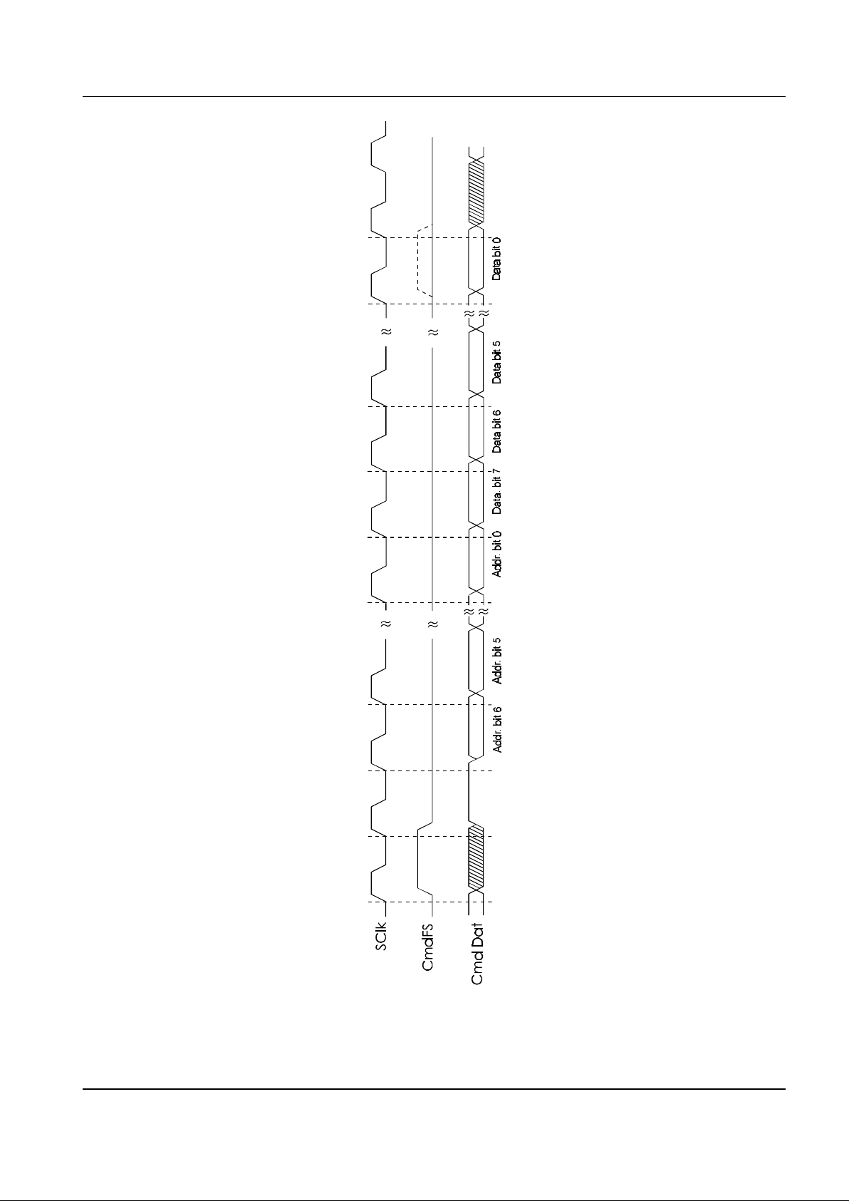
TETRA Baseband Processor FX980
1997 Consumer Microcircuits Limited 81 D/980/3
Figure 5b Command Write operation
Page 82

TETRA Baseband Processor FX980
1997 Consumer Microcircuits Limited 82 D/980/3
Figure 5c Bi-dir Command Read Operation
Page 83

TETRA Baseband Processor FX980
1997 Consumer Microcircuits Limited 83 D/980/3
Figure 5d Non bi-dir Command Read Operation
Page 84

TETRA Baseband Processor FX980
1997 Consumer Microcircuits Limited 84 D/980/3
Figure 5e Rx Data Serial Port Read Operation
Page 85

TETRA Baseband Processor FX980
1997 Consumer Microcircuits Limited 85 D/980/3
1.7.2 Packaging
Figure 6 L6 Mechanical Outline: Order as part no. FX980L6
Figure 7 FX980L7 Mechanical Outline: Order as part no. FX980L7
Page 86

TETRA Baseband Processor FX980
Handling precautions: This product includes input protection, however, precautions should be taken to
prevent device damage from electro-static discharge. CML does not assume any responsibility for the
use of any circuitry described. No IPR or circuit patent licences are implied. CML reserves the right at
any time without notice to change the said circuitry and this product specification. CML has a policy of
testing every product shipped using calibrated test equipment to ensure compliance with this product
specification. Specific testing of all circuit parameters is not necessarily performed.
CONSUMER MICROCIRCUITS LIMITED
1 WHEATON ROAD Telephone: +44 1376 513833
WITHAM - ESSEX Telefax: +44 1376 518247
CM8 3TD - ENGLAND e-mail: sales@cmlmicro.co.uk
http://www.cmlmicro.co.uk
 Loading...