

Page 1
CML Semiconductor Products
Tone Detector FX105A
D/105A/3 December 1995
1.0 Features Advance Information
•• Operates in High Noise Conditions •• Adjustable Bandwidth
•• ≥≥ 36dB Signal Input Range •• Adjustable Frequency
•• High Sensitivity •• Wide Voltage Range (2.7V to 5.5V)
•• Low Power •• Single and Multitone System
Applications
1.1 Brief Description
The FX105A is a monolithic CMOS tone operated switch, designed for tone decoding in single and
multitone signalling systems. The FX105A uses decoding techniques which allow a tone to be
recognised in the presence of high noise levels or strong adjacent signals. Detection centre frequency
and bandwidth can each be independently adjusted. The design is immune to high levels of harmonic
and sub-harmonic interference. Excellent noise immunity and constant bandwidth are maintained over
a wide range of input signal levels.
1996 Consumer Microcircuits Limited
Page 2

Tone Detector FX105A
CONTENTS
Section Page
1.0 Features..........................................................................................................1
1.1 Brief Description............................................................................................1
1.2 Block Diagram................................................................................................3
1.3 Signal List.......................................................................................................4
1.4 External Components....................................................................................5
1.5 General Description.......................................................................................6
1.6 Application Notes..........................................................................................7
1.6.1 General............................................................................................7
1.6.2 Method for Calculating External Component Values.......................7
1.7 Performance Specification .........................................................................12
1.7.1 Electrical Performance .................................................................. 12
1.7.2 Packaging......................................................................................14
1996 Consumer Microcircuits Limited 2 D/105A/3
Page 3
Tone Detector FX105A
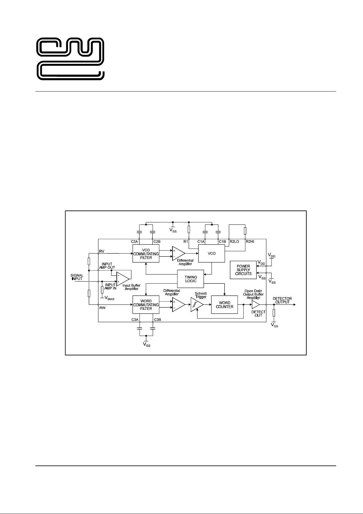
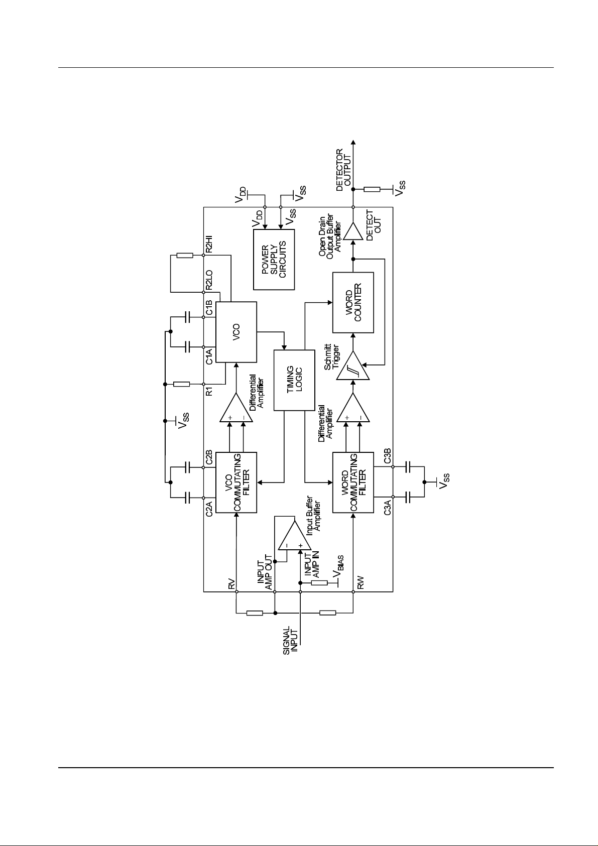
1.2 Block Diagram
Figure 1 Block Diagram
1996 Consumer Microcircuits Limited 3 D/105A/3
Page 4

Tone Detector FX105A
1.3 Signal List
Package
D4/P3
Signal Description
Pin No. Name Type
1 INPUT AMP IN I/P AC couple to this input of the input buffer
amplifier.
2 INPUT AMP OUT O/P The input buffer amplifier output.
3 RW I/P The input to the Detect/Word filter.
4 RV I/P The input to the VCO loop filter.
5 C3A O/P Word filter capacitor pin A.
6 C3B O/P Word filter capacitor pin B.
7 C2A O/P VCO Loop filter capacitor pin A.
8 C2B O/P VCO Loop filter capacitor pin B.
9 DETECT OUT O/P Open drain PMOS output, active on detect.
is required.
SS
10 V
SS
Note that a load resistor to V
Power Ground.
11 R2HI I/P Bandwidth control resistor pin A.
12 R2LO I/P Bandwidth control resistor pin B.
13 C1B O/P VCO capacitor B.
14 C1A O/P VCO capacitor A.
15 R1 I/P VCO discharge resistor. When potentiometer
tuning is required, a series resistor is
recommended to prevent possible shorting to
ground.
16 V
DD
Power Power supply.
Notes: I/P = Input
O/P = Output
1996 Consumer Microcircuits Limited 4 D/105A/3
Page 5
Tone Detector FX105A
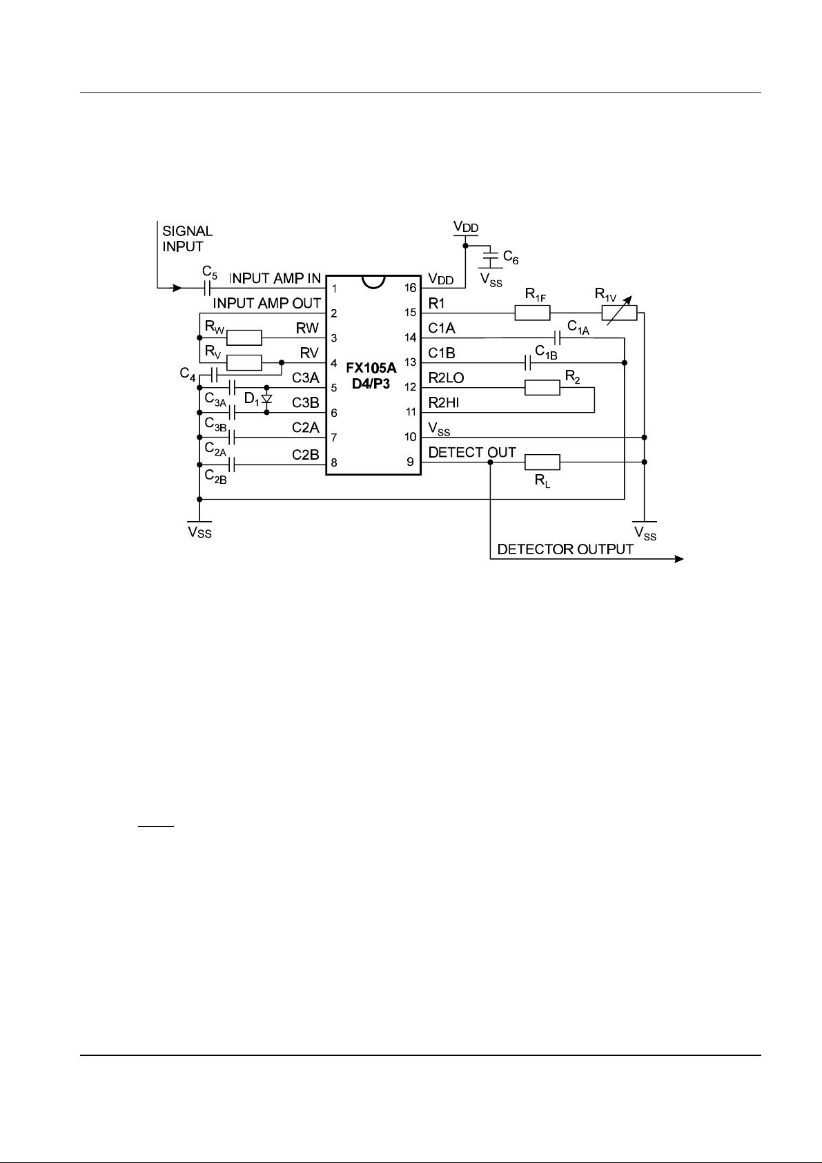
1.4 External Components
C
C
C
C
C
C
C
C
C
See section 1.6 R
1A
See section 1.6 R
1B
See section 1.6 R
2A
See section 1.6 R
2B
See section 1.6 R
3A
See section 1.6 R
3B
See section 1.6 D
4
0.27µF ±20%
5
0.1µF ±20%
6
1F
1V
2
L
V
W
1
See section 1.6
See section 1.6
See section 1.6
20kΩ ±20%
See section 1.6
See section 1.6
IN914 or similar
Notes: 1. For improved performance C4 may be chosen to provide 30° phase shift at the VCO
loop filter input.
2. For compatibility with the FX105P; capacitors (C1 .... C4) may be connected to V
DD
instead of VSS.
3. For improved de-response time, a diode (D
4. Any value load resistance (R
) may be used, providing the maximum load current does
L
) may be added.
1
not exceed the value given in section 1.7.1
Figure 2 Recommended External Components
1996 Consumer Microcircuits Limited 5 D/105A/3
Page 6

Tone Detector FX105A
1.5 General Description
The input signal to the FX105A is ac coupled to the buffer amplifier input, which is internally biased at
50% of supply voltage. The signal appears at the output of the buffer amplifier as an ac voltage
superimposed on the dc bias level. The signal is then coupled via R
oscillator (VCO) and word sampling switches, which cyclically connect C
four sample-and-hold RC circuit integrators. See Figure 3.
With no input signal level, each capacitor charges to the dc bias level so differential voltages are zero.
When an input signal is applied each capacitor receives an additional charge. This charge is
determined by the integrated average of the signal waveform during the time the capacitor is switched
into the circuit.
Figure 3 shows the operating sequence of the VCO sampling switches and their relationship to a
locked-on in-band signal. C
sample the input as it crosses the dc bias level. Should the signal not be locked to the VCO, a positive
or negative charge voltage will appear on C
applied to the VCO as an error correcting signal to enable the VCO to “lock.”
Figure 3 also shows the operating sequence of the “Word” sampling switches and their relationship to a
locked-on in-band signal. As the figure shows, the charge applied to C
and the charge applied to C
and C2B should not receive any additional charge since they always
2A
or C2B. This voltage, when differentially amplified, is
2A
should always be negative (with respect to the common bias level).
3B
and RW to the voltage controlled
V
and C3 into the circuit to form
2
should always be positive,
3A
These capacitor potentials are differentially amplified and applied to a dc comparator, which switches at
a pre-determined threshold voltage V
. The comparator output is a logic signal used to control a
TH
counter. This counter switches the FX105A output ON when the comparator output is maintained in
the “Word present” state for a minimum number of consecutive signal samples. The activated output
switch reduces the comparator threshold by 50%, introducing threshold hysteresis. Output chatter with
marginal input signal amplitudes is thereby minimised.
Figure 3 Sampling Clocks of Commutating Filters
1996 Consumer Microcircuits Limited 6 D/105A/3
Page 7

Tone Detector FX105A
1.6 Application Notes
1.6.1 General
The external components shown in Figure 2 are used to adjust the various performance parameters of
the FX105A. The signal-to-noise performance, response time and signal bandwidth are all interrelated
factors which should be optimised to meet the requirements of the application.
By selecting component values in accordance with the following formulae, optimum circuit performance
is obtained for any given application.
First define the following application parameters:
(a) The input frequency to be detected (f
this frequency by observing the output across C
is 6 x f
and the frequency observed at pins 13 or 14 (C1A or C1B) is 3 x f0).
0
). The free running frequency of the VCO is set to 6 times
0
or R1. (The frequency observed at pin 15 (R1)
1
(b) The FX105A Minimum Usable Bandwidth (MUBW). This is obtained by taking into account the
∆f
worst case tolerances (
frequency due to supply voltage (
) of the input frequency and the variations in the FX105A VCO
0
∆V
) and temperature (∆TEMP) variation of the FX105A and
DD
its supporting components.
(c) The maximum permissible FX105A response time.
(d) The minimum input signal amplitude.
(e) The maximum input signal amplitude.
Using this information the appropriate component values can be calculated, and the signal-to-noise
performance can be read from a chart. Do not add large safety margins for response time and
minimum signal amplitude: reasonable margins are already included in the formulae. Excessive
margins may result in reduced noise immunity.
1.6.2 Method for Calculating External Component Values
The example on the following pages demonstrates the calculation of component values for any given
application. For the purpose of this example, the values below are used:
(a) f
(b)
(c) Maximum allowed response time T
(d) Minimum input signal amplitude V
(e) Maximum input signal amplitude V
= 2800 Hz
0
∆TEMP = 100°C, ∆V
= 1V, ∆f0 = 0.5%
DD
ON
IN
MIN
IN
= 50msec
= 200 mVrms
= 400 mVrms
MAX
1.6.2.1 Calculate R
The components R
(C1A = C1B)
1C1
1
, C1A and C1B set the free running frequency of the VCO and therefore the f0 of the
FX105A. As shown below, the frequency of 2800 Hz corresponds to a capacitor value of 220 pF and a
resistor value of 385k
Ω. This resistance can be achieved with a 300 kΩ fixed resistor and a 100kΩ
potentiometer. R1 should lie in the range 100kΩ to 680kΩ.
= 1/ [2Kf0] = 1/ (2 x 2.1 x 2800) = 85µsec
R
1C1A
where K is a constant
the value of K increases with f
Therefore R
1996 Consumer Microcircuits Limited 7 D/105A/3
≈ 385kΩ for C1A = C1B = 220pF
1
= 2.1 ± 5%. Note that above f
up to a maximum of 2.5 at 20kHz.
0
= 1kHz,
0
Page 8

Tone Detector FX105A
≈
1.6.2.2 Calculate Minimum Usable Bandwidth (%)
Minimum Usable Bandwidth (MUBW) is the TOTAL (%) bandwidth required for the following:
∆f
(a) Input signal frequency tolerance (
(b) FX105A VCO temperature coefficient (T
(c) FX105A VCO supply voltage coefficient (V
)
0
= −100 ppm/ºC)
C
= 2330 ppm/V)
C
Add (a), (b) and (c) and express as TOTAL (%) bandwidth, not as a ± (%) value.
∆f
MUBW =
+ |Tc|∆TEMP + V
0
c∆VDD
MUBW = 0.5 + 0.01 x 100 + 0.233 x 1 ≈ 2%
1.6.2.3 Calculate the Recommended Operating Bandwidth
Note again that this is the TOTAL (%) bandwidth:
BW = ½ [10 + MUBW] = ½ (10 + 2) = 6%
1.6.2.4 Select R
for Operating BW
2
= 4.8 BW/ [10.35 −BW] = 4.8 x 6/ (10.35 −6) ≈ 6.8kΩ
R
2
The exact bandwidth given by any value of R2 will vary slightly. In applications where an exact
bandwidth is required, R
1.6.2.5 Calculate R
Therefore R
(C2A = C2B) Use nearest preferred values
VC2A
R
VC2A
V
should be a variable resistor to permit adjustment.
2
≈ 100/ [3 f0 BW] ≈ 100/ (3 x 2800 x 6) ≈ 2msec
200kΩ for C2A = C2B = 10nF
1.6.2.6 Define the Maximum Allowed Response Time
The maximum response time (T
time (T
). The FX105A’s TON must not exceed the maximum time allowed for the application, but
WORD
) is the sum of the VCO lock time (T
ON
a value lying near the maximum gives the best S/N performance.
(a) Calculate T
Note: T
LOCK
T
ON
.
LOCK
T
= 150/ [f0 BW] = 150/ (2800 x 6) ≈ 9msec
LOCK
may vary from near zero to the value given, causing corresponding variations in actual
) and the Word integration
LOCK
(b) Calculate Maximum Allowable T
T
WORD
= T
ON
MAX
Note: Since the maximum allowed response time (T
−T
WORD
= 50 - 9 = 41 msec
LOCK
) is 50 msec, a maximum Word integration time
ON
of 41 msec is available.
1996 Consumer Microcircuits Limited 8 D/105A/3
Page 9

Tone Detector FX105A
1.6.2.7 Calculate RWC3A (C3A = C3B) Use nearest preferred values.
R
WC3A
≈ T
/ [−3In (1 - VTH/ V
WORD
A signal amplitude of 200 mV and a resistor value R
will yield a T
time of 20msec. This in turn yields a response time of 9msec + 20msec = 29msec.
WORD
1.6.2.8 Calculate the Maximum De-response Time
≈ −3 RWC3A In (VTH/ V
T
OFF
For improved de-response time, a diode (1N914 or similar) can be placed between pins 5 and 6, as
shown in Figure 2. The formula and figure below show the approximate time the FX105A will take to
turn off after an in-band signal has been removed. The effect of this diode is to greatly reduce the turnoff time with signal input amplitudes greater than 300 mV
then KDT increases.
≈ KDTRWC
T
OFF
3A
So for a maximum signal amplitude of 400mV, a resistor value RW of 510kΩ with a 0.1µF capacitor for
and C3B and a diode between pins 5 and 6, a de-response time of ≈ 182 msec is obtained.
C
3A
) ] where VTH is the word filter
IN
MIN
sensitivity, see Section 1.7.1
of 510kΩ with a 0.1µF capacitor for C3A and C
W
) where VTH is the word filter
IN
MAX
sensitivity, see Section 1.7.1
. Figure 4 is for VDD = 5V; for lower V
rms
3B
DD
Figure 4 KDT Factor for T
1996 Consumer Microcircuits Limited 9 D/105A/3
vs. Signal Input Amplitude
OFF
Page 10

Tone Detector FX105A
1.6.2.9 Calculate Signal to Noise Performance
Worst-case S/N calculations depend on calculation of a value “M” using the formula shown below:
WC3A
/ [3 RVC2A]
M = R
substituting our example values,
M = 510 x 0.1/ (3 x 200 x 0.01) = 8.5
By substituting this value for M in Figure 5 the minimum required S/N of an in band tone with respect to
an adjacent interfering tone can be found. This has to be increased if the required tone amplitude is
close to the word filter sensitivity V
TH
.
Figure 5 S/N vs. BW Separation
The following formula expresses the reduction in noise immunity as the input signal approaches the
word filter sensitivity V
required S/N = 20 log (V
TH
.
/ [VIN - VTH] ) + S/N
IN
Figure 5
If this S/N is better than required for the application, RWC3A can be reduced, or the operating
bandwidth can be increased to obtain a faster tone detection time.
If the S/N performance is not adequate, the operating bandwidth can be reduced toward the MUBW,
or R
can be increased to improve S/N performance at the expense of a slower response time.
WC3A
1.6.2.10 Calculation of PLL Filter Phase Shift
Capacitor C
is used to phase shift the input to the VCO commutating filter by 30°, thus shifting the
4
sampling clocks by the same amount. This enables the "Word" sampling filter to sample and integrate
at the maxima and minima of the input tone.
= tan (30°) / [2π f0 RV] ≈ 0.092 / [f0 RV] ≈ 164pF
C
4
1996 Consumer Microcircuits Limited 10 D/105A/3
Page 11

Tone Detector FX105A
1.7 Performance Specification
1.7.1 Electrical Performance
Absolute Maximum Ratings
Exceeding these maximum ratings can result in damage to the device.
Min. Max. Units
Supply (VDD - VSS) -0.3 7.0 V
Voltage on any pin to V
Current into or out of V
SS
DD
and V
pins -30 +30 mA
SS
-0.3 V
Current into or out of any other pin -20 +20 mA
Maximum Output Switch Load Current +10 mA
P3/D4 Package Min. Max. Units
Total Allowable Power Dissipation at Tamb = 25°C 800 mW
... Derating 13 mW/°C
Storage Temperature -55 +125 °C
Operating Temperature -30 +85 °C
+ 0.3 V
DD
Operating Limits
Correct operation of the device outside these limits is not implied.
Notes Min. Max. Units
Supply (VDD - VSS) 2.7 5.5 V
Operating Temperature -30 +85 °C
1996 Consumer Microcircuits Limited 11 D/105A/3
Page 12

Tone Detector FX105A
Operating Characteristics
For the following conditions unless otherwise specified:
= 3.0V to 5.0V, Tamb = −40°C to +85°C, Load resistance on decoder output pin = 20kΩ
V
DD
Notes Min. Typ. Max. Units
Static Parameters
I
DD
Amplifier Input Impedance 200
2 0.9 3.0 mA
k
Digital Output Impedance 500
Analogue Output Impedance 1000
Dynamic Parameters
Input Signal
Amplitude 2 1.0 Vrms
Frequency 40 20,000 Hz
Response Threshold 1 18 38 mVrms
Deresponse Threshold 1 5 9 mVrms
BW Range 5 10 %f
Signal to Noise Performance -6 -9 dB
/2) Subharmonic Rejection 30 dB
(f
0
) Harmonic Rejection 20 dB
(5 f
0
Ω
Ω
Ω
0
VCO
Frequency 3 240 120,000 Hz
Frequency Stability (
Frequency Stability (
∆ TEMP) 3 100 ppm/°C
∆ V
) 3 2330 ppm/V
DD
Amplifier
Open Loop Gain 60 dB
Gain Bandwidth Product 1.0 MHz
Closed Loop Gain 0 dB
Word Commutating Filter
Sensitivity (V
) 4 12.5 mVrms
TH
Notes: 1. With diode (D1) fitted.
2. For V
= 5V. Multiply by VDD/5V for other supply values.
DD
3. Observing pins 13, 14 or 15 (D4/P3 package) will cause a frequency shift due to additional
loading. If tuning the centre frequency by observing the VCO, design in a buffer amplifier
between pin 15 and the probe/calibration point and tune with no input signal. Otherwise, tune
by observing the detect output band edges while sweeping the input signal.
4. Adjust according to equation for R
in Section 1.6.2.
2
1996 Consumer Microcircuits Limited 12 D/105A/3
Page 13

Tone Detector FX105A
1.7.2 Packaging
Figure 6 - SOIC Mechanical Outline: Order as part no. FX105AD4
Figure 7 - DIL Mechanical Outline: Order as part no. FX105AP3
1996 Consumer Microcircuits Limited 13 D/105A/3
Page 14

Tone Detector FX105A
Handling precautions: This product includes input protection, however, precautions should be taken to prevent
device damage from electro-static discharge. CML does not assume any responsibility for the use of any
circuitry described. No IPR or circuit patent licences are implied. CML reserves the right at any time without
notice to change the said circuitry and this product specification. CML has a policy of testing every product
shipped using calibrated test equipment to ensure compliance with this product specification. Specific testing
of all circuit parameters is not necessarily performed.
CONSUMER MICROCIRCUITS LIMITED
1 WHEATON ROAD Telephone: +44 1376 513833
WITHAM - ESSEX CM8 3TD - ENGLAND Telefax: +44 1376 518247
 Loading...