

Page 1
SANYO Electric Co.,Ltd. Semiconductor Bussiness Headquaters
TOKYO OFFICE Tokyo Bldg., 1-10, 1 Chome, Ueno, Taito-ku, TOKYO, 110-8534 JAPAN
N-Channel Silicon MOSFET
DC-DC Converter Applications
Ordering number:EN5579A
FW211
Features
· Low ON resistance.
· 2.5V drive.
Specifications
Absolute Maximum Ratings at Ta = 25˚C
retemaraPlobmySsnoitidnoCsgnitaRtinU
egatloVecruoS-ot-niarDV
egatloVecruoS-ot-etaGV
)CD(tnerruCniarDI
)eslup(tnerruCniarDI
noitapissiDrewoPelbawollAP
noitapissiDlatoTP
erutarepmeTlennahChcT 051
erutarepmeTegarotSgtsT 051+ot55–
D
D
T
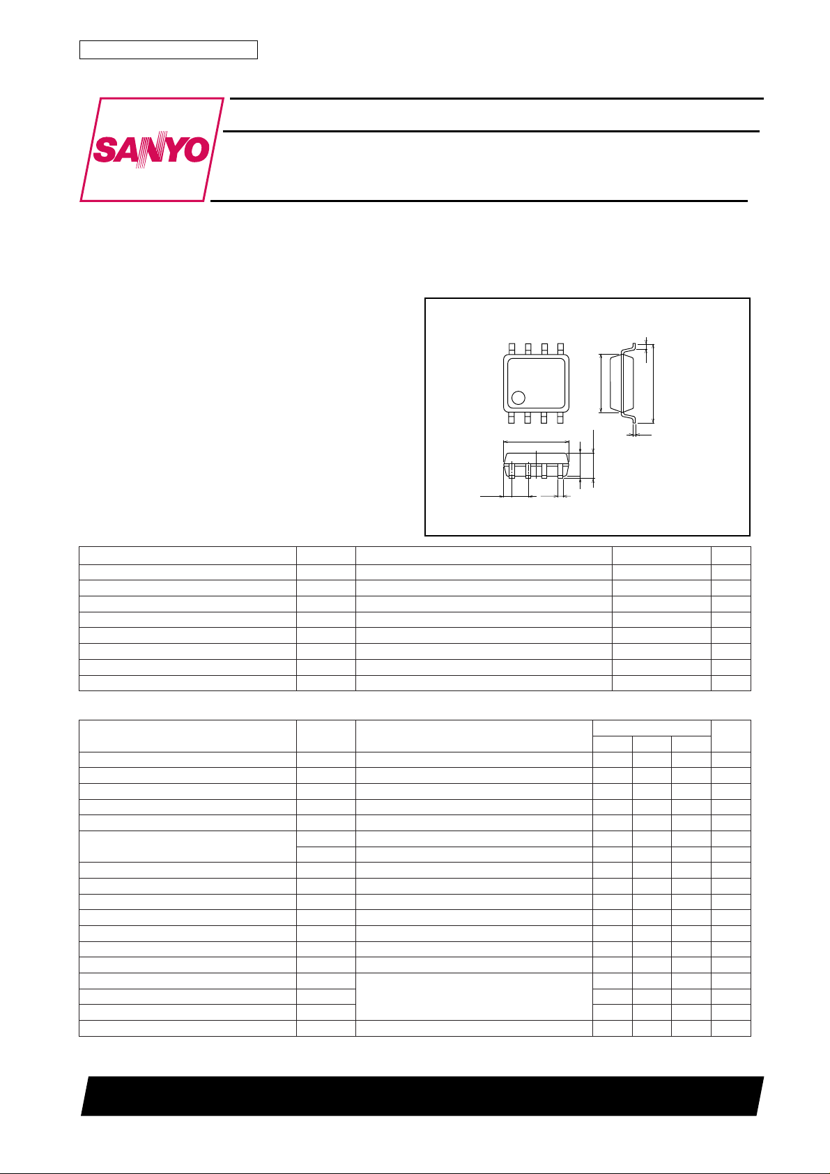
Package Dimensions
unit:mm
2129
[FW211]
58
4.4
14
1.27
0.595
SSD
SSG
PW≤10µs, duty cycle≤1%
PD
Mounted on a ceramic board (1000mm2×0.8mm) 1unit
Mounted on a ceramic board (1000mm2×0.8mm)
5.0
0.43
1.8max
1.5
0.1
0.3
6.0
1:Source 1
2:Gate 1
3:Source 2
0.2
4:Gate 2
5:Drain 2
6:Drain 2
7:Drain 1
8:Drain 1
SANYO:SOP8
02V
01±V
6A
25A
7.1W
0.2W
˚C
˚C
Electrical Characteristics at Ta=25˚C
retemaraPlobmySsnoitidnoC
egatloVnwodkaerBecruoS-ot-niarDV
tnerruCniarDegatloVetaGoreZI
tnerruCegakaeLecruoS-ot-etaGI
egatloVffotuCV
ecnattimdArefsnarTdrawroF|sfy|VSDI,V01=
ecnatsiseRetatS-NOecruoS-ot-niarDcitatS
R
R
ecnaticapaCtupnIssiCV
ecnaticapaCtuptuOssoCV
ecnaticapaCrefsnarTesreveRssrCV
emiTyaleDNO-nruTt
emiTesiRt
emiTyaleDFFO-nruTt
emiTllaFt
egrahCetaGlatoTgQ
egrahCecruoS-ot-etaGsgQ 5Cn
egrahC"relliM"niarD-ot-etaGdgQ 7Cn
egatloVdrawroFedoiDV
SSD
SSG
r
f
DS
SSD)RB(
)ffo(SG
1IDV,A5=
)no(SD
2IDV,A2=
)no(SD
)no(d
)ffo(d
I
V
V
V
V
I
V,Am1=
D
SD
SG
SD
SD
SD
SD
SD
S
0=02V
SG
V,V02=
0=001Aµ
SG
V,V8±=
0=01±Aµ
SD
I,V01=
Am1=4.03.1V
D
A5=951S
D
V4=7253mΩ
SG
V5.2=5384mΩ
SG
zHM1=f,V01=057Fp
zHM1=f,V01=025Fp
zHM1=f,V01=003Fp
tiucriCtseTdeificepSeeS02sn
tiucriCtseTdeificepSeeS002sn
tiucriCtseTdeificepSeeS051sn
tiucriCtseTdeificepSeeS051sn
V,V01=
V,A5=
SG
I,V01=
SG
D
0=0.12.1V
sgnitaR
nimpytxam
03Cn
A1=
tinU
61598TS (KOTO) TA-0861 No.5579-1/3
Page 2
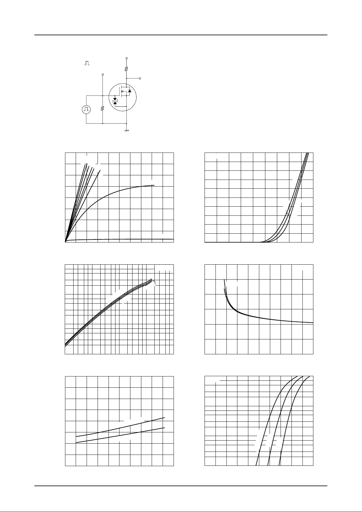
Switching Time Test Circuit
V
4V
0V
PW=10µs
D.C.≤1%
IN
V
VDD=10V
ID=5A
IN
G
RL=2Ω
D
V
FW211
OUT
–A
D
Drain Current, I
100
–S
fs |
y
|
10
1.0
8
7
6
5
4
3
2
1
0
0 0.1
7
5
3
2
7
5
3
2
7
P.G
8V
6V
4V
3V
2.5V
50Ω
ID-
2V
FW211
S
V
DS
1.5V
0.2 0.3 0.4 0.5 0.6 0.7 0.8 0.9 1.0
Drain-to-Source Voltage,VDS–V
|yfs|
Ta=
25˚C
-
-
75˚C
I
D
25˚C
VGS=1V
VDS=10V
10
–A
D
Drain Current, I
60
50
–mΩ
)
on
40
DS (
30
20
VDS=10V
9
8
7
6
5
4
3
2
1
0
0 0.2
ID-
V
GS
75˚C
25˚C
-
Ta=
0.4 0.6 0.8 1.0 1.2 1.4 1.6 1.8
Gate-to-Source Voltage, V
R
(on)
DS
-
–V
GS
V
GS
Tc=25˚C
ID=5A
2A
25˚C
Forward Transfer Admittance,
0.1
2233557
0.01
0.1
Drain Current, ID–A
80
70
–mΩ
60
)
on
50
DS (
40
30
20
10
Static Drain-to-Source
ON-State Resistance, R
0
-60 -40
-20 0 20 40 60 80 100 120 140
Case Temperature, Tc – ˚C
2357
R
(on)
DS
I
D
I
D
23 57102357
1.0
-
Tc
=2.5V
GS
=2A,V
=4V
GS
=5A,V
Static Drain-to-Source
100
10
ON-State Resistance, R
0
01
10
VGS=0
7
5
3
2
–A
1.0
F
7
5
3
2
0.1
7
Forward Current, I
5
3
2
0.01
0 0.1 0.2 0.3 0.4 0.5 0.6 0.7 0.8 0.9 1.0
2345678910
Gate-to-Source Voltage, V
IF-
V
Ta=75˚C
Diode Forward Voltage, V
SD
25˚C
GS
SD
25˚C
-
–V
–V
No.5579-2/3
Page 3

FW211
,,,,,,,
,,,,,,,
,,,,,,,
10000
7
5
3
2
1000
7
5
Ciss,Coss,Crss – pF
3
2
100
02468101214161820
Ciss,Coss,Crss
-
V
DS
f=1MHz
Ciss
Coss
Crss
10
9
8
–V
GS
7
6
5
4
3
2
Gate-to-Source Voltage, V
1
0
VDS=10V
VGS-
=1A
I
D
0
5 1015202530
Qg
Drain-to-Source Voltage,VDS– V Total Gate Charge, Qg – nC
1000
Switching Time, SW Time – ns
100
7
5
3
2
7
5
3
2
10
0.1
SW Time
23 577
Drain Current, ID–A
P
(FET2)
2.0
1.8
1.6
(FET2) – W
1.4
D
1.2
1.0
0.8
0.6
0.4
0.2
Allowable Power Disipation, P
0
0 0.2
D
Mounted ceramic board (1000mm
0.4 0.6 0.8 1.0 1.2 1.4 1.6 1.8 2.0
Allowable Power Disipation, PD (FET1) – W
-
I
D
23 57102
1.0
-
P
(FET1)
D
2
t
t
d(off)
t
×0.8mm)
VDD=10V
=4V
V
GS
r
f
t
d(on)
100
7
IDP=52A
5
3
2
10
ID=6A
–A
7
D
5
3
2
1.0
Operation in this
area is limited
7
(on).
by R
DS
5
Drain Current, I
Ta=25˚C
2
1pulse
0.1
1unit
7
Mounted ceramic board (1000mm2×0.8mm)
5
233
7
5
A S O
DC operation
1.0
23 2357
Drain-to-Source Voltage, VDS–V
2.5
– W
2.0
D
1.7
1.5
1.0
0.5
PD-
Total Dissipation
1 unit
Allowable Power Disipation, P
Mounted ceramic board (1000mm2×0.8mm)
0
020
40 60 80 100 120 140 160
Ambient Temperature, Ta – ˚C
100ms
Ta
No products described or contained herein are intended for use in surgical implants, life-support systems,
aerospace equipment, nuclear power control systems, vehicles, disaster/crime-prevention equipment and
the like, the failure of which may directly or indirectly cause injury, death or property loss.
Anyone purchasing any products described or contained herein for an above-mentioned use shall:
Accept full responsibility and indemnify and defend SANYO ELECTRIC CO., LTD., its affiliates,
subsidiaries and distributors and all their officers and employees, jointly and severally, against any
and all claims and litigation and all damages, cost and expenses associated with such use:
Not impose any responsibilty for any fault or negligence which may be cited in any such claim or
litigation on SANYO ELECTRIC CO., LTD., its affiliates, subsidiaries and distributors or any of
their officers and employees jointly or severally.
Information (including circuit diagrams and circuit parameters) herein is for example only; it is not guaranteed for volume production. SANYO believes information herein is accurate and reliable, but no guarantees
are made or implied regarding its use or any infringements of intellectual property rights or other rights of
third parties.
10ms
1ms
10
10µs
100
µs
This catalog provides information as of June, 1998. Specifications and information herein are subject to
change without notice.
PS No.5579-3/3
 Loading...