

Page 1

E
June 1997 Order Number 241997-010
Max. Operating Frequency
75
MHz
90
MHz
100
MHz
120
MHz
133
MHz
150
MHz
166
MHz
200
MHz
iCOMP® Index 2.0 Rating 67 81 90 100 111 114 127 142
Note: Contact Intel Corporation for more information about iCOMP®Index 2.0 ratings.
n
Compatible with Large Software Base
MS-DOS*, Windows*, OS/2*, UNIX*
n
32-Bit CPU with 64-Bit Data Bus
n
Superscalar Architecture
Two Pipelined Integer Units Are Capable
of 2 Instructions/Clock
Pipe-lined Floating Point Unit
n
Separate Code and Data Caches
8-Kbyte Code, 8-Kbyte Write Back Data
MESI Cache Protocol
n
Advanced Design Features
Branch Prediction
Virtual Mode Extensions
n
3.3V BiCMOS Silicon Technology
n
4-Mbyte Pages for Increased TLB Hit Rate
n
IEEE 1149.1 Boundary Scan
n
Dual Processing Configuration
n
Functional Redundancy Checking Support
n
Internal Error Detection Features
n
Multi-Processor Support
Multiprocessor Instructions
Support for Second Level Cache
n
On-Chip Local APIC Controller
MP Interrupt Management
8259 Compatible
n
Upgradable with a Pentium® OverDrive
®
Processor
n
Power Management Features
System Management Mode
Clock Control
n
Fractional Bus Operation
200-MHz Core/66-MHz Bus
166-MHz Core/66-MHz Bus
150-MHz Core/60-MHz Bus
133-MHz Core/66-MHz Bus
120-MHz Core/60-MHz Bus
100-MHz Core/66-MHz Bus
100-MHz Core/50-MHz Bus
90-MHz Core/60-MHz Bus
75-MHz Core/50-MHz Bus
The Pentium
®
processor 75/90/100/120/133/150/166/200 extends the Pentium processor family, providing
performance needed for mains tream des k top applic ations as w ell as for works tations and s erv ers . The Pentium
process or is compatible with the entire installed base of applications for DOS*, W indows*, OS/2* , and UNIX*.
The Pentium process or 75/90/100/120/133/150/166/200 superscalar architecture can execute two instructions
per clock c y c le. B ranc h predic tion and s epar ate c ac hes als o inc reas e per formanc e. The pipelined floating point
unit delivers workstation level performance. Separate code and data caches reduce cache conflicts while
remaining software transparent. The Pentium processor 75/90/100/120/133/150/166/200 has 3.3 million
transistors and is built on Intel’s advanced 3.3V BiCMOS silicon technology. The Pentium processor
75/90/100/120/133/150/166/200 has on-chip dual process ing support, a loc al multiproces sor interr upt controller,
and SL power management features. The Pentium process or may contain design defec ts or errors know n as
errata which may cause the produc t to deviate from published s pecifications. Current c haracterized errata are
available upon request.
PENTIUM® PROCESSOR
Page 2

CONTENTS
PAGE PAGE
1.0. MICROPROCESSOR ARCHITECTURE
OVERVIEW .......................................................3
1.1. Pentium® Processor Family Architecture......3
1.2. Pentium® Processor
75/90/100/120/133/150/166/200....................6
2.0. PINOUT..............................................................8
2.1. Pinout and Pin Descriptions...........................8
2.2. Design Notes................................................12
2.3. Quick Pin Reference....................................12
2.4. Pin Reference Tables...................................22
2.5. Pin Grouping According to Function............26
3.0. ELECTRICAL SPECIFICATIONS ..................27
3.1. Electrical Differences Between Pentium®
Processor 75/90/100/120/133/150/166/200
and Pentium Processor 60/66......................27
3.2. Absolute Maximum Ratings..........................28
3.3. DC Specifications.........................................28
3.4. AC Specifications.........................................31
4.0. MECHANICAL SPECIFICATIONS.................56
5.0. THERMAL SPECIFICATIONS........................62
5.1. Measuring Thermal Values..........................62
6.0. OverDrive® PROCESSOR SOCKET
SPECIFICATION.............................................69
6.1. Introduction...................................................69
6.2. Socket 5.......................................................69
6.3. Socket 7.......................................................70
Information in this document is provided in connection with Intel products. No license, express or implied, by estoppel or
otherwise, to any intellectual property rights is granted by this document. Except as provided in Intel’s Terms and Conditions of
Sale for such products , Intel assumes no liability w hats oeve r, and Intel disc laims any expres s or implied warranty , relating to
sale and/or use of Intel products including liability or warr anties re lating to fitnes s fo r a par tic ular pur pose, me rchantabilit y, or
infringement of any patent, copyright or other intellectual property right. Intel produc ts are not intended for us e in medical, life
saving, or life sustaining applications.
Intel may make changes to specifications and product descriptions at any time, without notice.
Designers must not r ely on the absence or c haracteristics of any features or instruc tions marked "reser ved" or "undefined."
Intel reserves these for future definition and shall have no responsibility whatsoever for conflicts or incompatibilities arising from
future changes to them.
The Pentium
®
processor may contain design defects or errors know n as errata whic h may caus e the product to deviate from
published specifications. Current characterized errata are available on request.
Contact your local Intel sales office or your distributor to obtain the latest specifications and before placing your product order.
Copies of documents which hav e an ordering number and are refer enced in this document, or other Intel literatur e, may be
obtained from:
Intel Corporation
P.O. Box 7641
Mt. Prospect IL 60056-7641
or call 1-800-879-4683
or visit Intel’s website at http:\\www.intel.com
Copyright © Intel Corporation 1993, 1996, 1997.
* Third-party brands and names are the property of their respective owners.
Page 3

E
PENTIUM® PROCESSO R 75/ 90/100/120/133/150/ 166/ 200
3
1.0. MICROPROCESSOR
ARCHITECTURE OVERVIEW
The Pentium® processor 75/90/100/120/133/
150/166/200 extends the Intel Pentium family of
microprocessors. It is binary compatible with the
8086/88, 80286, Intel386™ DX CPU, Intel386 SX
CPU, Intel486™ DX CPU, Intel486 SX CPU,
Intel486 DX2 CPU, and Pentium processor 60/66.
The Pentium processor family consists of the
following products.
• Described in this document (product code
80502). The name “Pentium processor
75/90/100/120/133/150/166/200” will be us ed to
refer to these products:
– Pentium processor at 200 MHz, iCOMP
®
Index 2.0 rating = 142
– Pentium processor at 166 MHz, iCOMP
Index 2.0 rating = 127
– Pentium processor at 150 MHz, iCOMP
Index 2.0 rating = 114
– Pentium processor at 133 MHz, iCOMP
Index 2.0 rating = 111
– Pentium processor at 120 MHz, iCOMP
Index 2.0 rating = 100
– Pentium processor at 100 MHz, iCOMP
Index 2.0 rating = 90
– Pentium processor at 90 MHz, iCOMP
Index 2.0 rating = 81
– Pentium processor at 75 MHz, iCOMP
Index 2.0 rating = 67
• Original Pentium processor. The name
“Pentium process or 60/66” will be used to refer
to the original 60 and 66 MHz version products:
– Pentium processor at 66 MHz, iCOMP
Index 2.0 rating = 57
– Pentium processor at 60 MHz, iCOMP
Index 2.0 rating = 51
The Pentium proces sor f amily arc hitectur e c ontains
all of the features of the Intel486 CPU family, and
provides significant enhancements and additions
including the following:
• Superscalar Architecture
• Dynamic Branch Prediction
• Pipelined Floating-Point Unit
• Improved Instruction Execution Time
• Separate 8K Code and 8K Data Caches
• Writeback MESI Protocol in the Data Cache
• 64-Bit Data Bus
• Bus Cycle Pipelining
• Address Parity
• Internal Parity Checking
• Functional Redundancy Checking
• Execution Tracing
• Performance Monitoring
• IEEE 1149.1 Boundary Scan
• System Management Mode
• Virtual Mode Extensions
In addition to the features listed abov e, the Pentium
processor 75/90/100/120/133/150/166/200 offers
the following enhancements over Pentium
processor 60/66:
• Fractional bus operation allowing higher core
frequency operation
• Dual processing support
• SL power management features
• On-chip local APIC device
1.1. Pentium® Processor Family
Architecture
The application instruction set of the Pentium
processor family includes the complete Intel486
CPU family instruction set with extensions to
accommodate s ome of t he additional func tionalit y of
the Pentium processors. All application software
written for the Intel386 and Intel486 family
microproc es s ors will run on the Pentium proc es s ors
without modification. The on-chip memory
management unit (MMU) is completely compatible
with the Intel386 family and Intel486 family of CPUs.
The Pentium processors implement several
enhancements to increase performance. The two
instruction pipelines and floating-point unit on
Pentium processors are capable of independent
operation. Each pipeline issues frequently used
Page 4

PENTIUM® PROCESSOR 75/90/100/120/133/150/166/200
E
4
instructions in a single clock. Together, the dual
pipes can issue two integer instructions in one
clock , or one floating point ins t ruc tion ( under c er tain
circumstances, two floating-point instructions) in
one clock.
Branch prediction is implemented in the Pentium
processors. To support this, Pentium processors
implement two prefetch buffers, one to prefetch
code in a linear fashion, and one that prefetches
code according to the BTB so the needed code is
almost always prefetched before it is needed for
execution.
The floating-point unit has been completely
redesigned over the Intel486 CPU. Faster
algorithms prov ide up to 10X speed- up for common
operations including add, multiply, and load.
Pentium processors include separate code and data
caches integrated on-chip to meet performance
goals. Each cache is 8 Kbytes in size, with a 32byte line size and is 2-way set associative. Each
cache has a dedicated Translation Lookaside Buffer
(TLB) to translate linear addresses to physical
addresses. The data cache is configurable to be
write back or write through on a line-by-line basis
and follows the MES I prot oc ol. The data cache t ags
are triple ported to support two data trans fers and
an inquire cycle in the same clock. The code cache
is an inherently write-protected cache. The code
cache tags are also triple ported to support
snooping and split line ac cesses. Individual pages
can be configured as cacheable or non-cacheable
by software or hardware. The caches can be
enabled or disabled by software or hardware.
The Pentium processors have increased the data
bus to 64 bits to improve the data transfer rate.
Burst read and burst write back cycles are
supported by the Pentium processors. In addition,
bus cycle pipelining has been added to allow two
bus cycles to be in progress simultaneously. The
Pentium processors' Memory Management Unit
contains optional extensions to the architecture
which allow 2-Mbyte and 4-Mbyte page sizes.
The Pentium processors have added significant
data integrity and error detection capability. Data
parity chec king is still s upported on a byte-by -byte
basis. Address parity checking, and internal parity
checking features have been added along with a
new exception, the machine check exception.
In addition, the Pentium processors have
implemented functional redundancy checking to
provide maximum error detection of the processor
and the interface to the proc ess or. When func tional
redundancy chec king is us ed, a second proc essor,
the “checker” is us ed to execute in loc k step w ith
the “master” processor. The checker samples the
master's outputs and compares those values with
the values it computes internally, and asserts an
error signal if a mismatch occurs.
As more and more functions ar e integrated on c hip,
the complexity of board level testing is increased.
To address this, the Pentium processors have
increased test and debug capability. The Pentium
processors implement IEEE Boundary Scan
(Standard 1149.1). In addition, the Pentium
processors have specified 4 breakpoint pins that
correspond to each of the debug registers and
externally indicate a breakpoint match. Execution
tracing provides external indications when an
instruc tion has completed ex ecution in either of the
two internal pipelines, or when a branch has been
taken.
System Management Mode (SMM) has been
implemented along with some extensions to the
SMM architecture. Enhancements to the virtual
8086 mode have been made to increase
performance by reduc ing the number of times it is
necessary to trap to a virtual 8086 monitor.
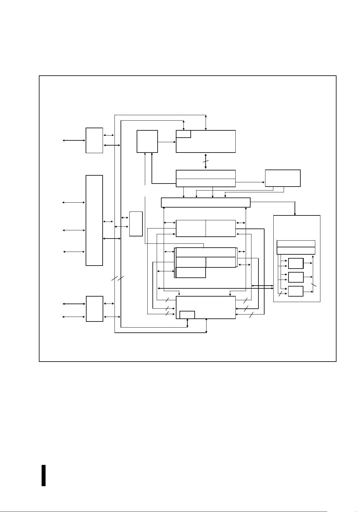
Figure 1 shows a block diagram of the Pentium
processor 75/90/100/120/133/150/166/200.
Page 5
E
PENTIUM® PROCESSO R 75/ 90/ 100/ 120/ 133/ 150/ 166/ 200
5
Branch
Target
Buffer
Code Cache
8 KBytes
ROM
Control Unit
Generate
Address
Generate
Data Cache
8 KBytes
256
TLB
TLB
Prefetch
Address
Prefetch Buffers
Instruction Decode
Instruction
Pointer
Integer Register File
ALU
Barrel Shifter
32
32
32
32
32
32
Page
Unit
Bus
Unit
64-Bit
Data
Bus
32-Bit
Address
Bus
Control
64-Bit
Data
Bus
32-Bit
Addr.
Bus
64
Control
Register File
Add
Multiply
Divide
Floating
Point
Unit
Pentium® Processor (75/90/100/120/133/150/166/200 MHz)
Control
80
80
Address
(U Pipeline) (V Pipeline)
(U Pipeline)
(V Pipeline)
ALU
Branch Verification
and Target Address
32
DP
Logic
Control
APIC
Data
Control
199718
Figure 1. Pentium® Processor Block Diagram
The block diagram shows the two instruction
pipelines, the "u” pipe and the "v” pipe. The u-pipe
can execute all integer and floating point
instructions. The v-pipe can execute simple integer
instructions and the FXCH floating-point
instructions.
The separate code and data caches are shown.
The data cache has two port s, one for eac h of the
two pipes (the tags are triple ported to allow
simultaneous inquir e cycles). The data cache has
a dedicated Trans lation Lookaside Buff er (TLB) t o
translate linear addresses to the physical
addresses used by the data cache.
The code cache, br anch target buf fer and prefetc h
buffers are responsible for getting raw instr uctions
into the execut ion units of the Pentium proc essor.
Instructions are fetched from the code cache or
from the external bus. Branch addresses are
remembered by the branc h t arget buf fer. The c ode
cache TLB trans lates linear addres ses to phy sical
addresses used by the code cache.
Page 6

PENTIUM® PROCESSOR 75/90/100/120/133/150/166/200
E
6
The decode unit decodes the prefetched
instructions so the Pentium processors can
execute the ins truc tion. The cont rol ROM cont ains
the microcode which controls the sequence of
operations that must be performed to implement
the Pentium processor architecture. The control
ROM unit has direct control over both pipelines.
The Pentium processors contain a pipelined
floating-point unit that provides a significant
floating-point performance advantage over
previous generations of processors.
The architectural features introduced in this
chapter are more fully described in the
Pentium
®
Processor Family Developer’s Manual, Volume 1
(Order Number 241428).
1.2. Pentium® Processor
75/90/100/120/133/150/166/200
In addition to the architec ture desc ribed above for
the Pentium processor family, the Pentium
processor 75/90/100/120/133/150/166/200 has
additional features which are described in this
section.
The Pentium processor 75/90/100/120/133/
150/166/200 offers higher perfor mance and higher
operating frequencies than the Pentium process or
60/66.
Symmetric dual processing in a system is
supported with two Pentium processor
75/90/100/120/133/150/166/200. The two
processors appear to the system as a single
Pentium processor 75/90/100/120/133/150
/166/200. Operating systems with dual processing
support properly schedule computing tasks
between the two processors. This scheduling of
tasks is transparent to software applications and
the end-user. Logic built into the processors
support a “glueless” interface for easy system
design. Through a private bus, the two Pentium
processor 75/90/100/120/133/150/166/200
arbitrate for the external bus and maintain cache
coherency. Dual processing is supported in a
system only if both processors are operating at
identical core and bus frequencies.
In this document, in order to distinguish between
two Pentium processor 75/90/100/120/133/
150/166/200 in dual processing mode, one CPU
will be designated as the “Primary” processor and
the other as the “Dual” pr oces sor. N ote that this is
a different concept than that of “master” and
“checker” processors described above in the
discussion on functional redundancy.
Due to the advanc ed 3.3V BiC MOS pr oc es s that it
is produced on, the Pentium processor
75/90/100/120/133/150/166/200 dissipates less
power than the Pentium processor 60/66. In
addition to the SMM features des cr ibed above, the
Pentium processor 75/90/100/120/133/150/
166/200 supports cloc k c ontrol. When the cloc k to
the Pentium processor 75/90/100/120/133/150/
166/200 is stopped, power dissipation is virtually
eliminated. The combination of these
improvements makes the Pentium processor
75/90/100/120/133/150/166/200 a good choic e for
energy-efficient desktop designs.
Supporting an upgrade soc ket (Sock et 5/7) in the
system will provide end-user upgradability by the
addition of a Pentium OverDrive processor. Typical
applications will realize a 40%–70% performance
increase by addition of a Pentium OverDrive
processor.
Socket 7 has been defined as the upgrade soc ket
for the Pentium proc essor 75/90/100/120/133/150/
166/200. The flexibility of the Socket 7 definition
makes it backward compatible with Soc ket 5 and
should be used for all new Pentium processorbased system designs.
The Pentium processor 75/90/100/120/133/
150/166/200 supports fractional bus operation.
This allows the internal proces sor core to operate
at high frequencies, while communic ating with the
external bus at lower frequencies.
The Pentium processor 75/90/100/120/133/
150/166/200 contains an on-chip Advanced
Programmable Interrupt Controller (APIC). This
APIC implementation supports multiprocessor
interrupt management (with symmetric interrupt
distribution across all processors), multiple I/O
subsystem support, 8259A compatibility, and interprocessor interrupt support.
Page 7

E
PENTIUM® PROCESSO R 75/ 90/100/120/133/150/ 166/ 200
7
1.3. Pentium® Processors with
Voltage Reduction
Technology
Currently, Intel's Pentium processor with Voltage
Reduction Tec hnology family cons ists of two s ets
of products. Please reference the appropriate
datasheets f or c orr ec t pinout, mec hanic al, ther mal,
and electrical specifications. Detailed information
on Mobile Pentium processors based on 0.6 µm
process technology (75, 90, and 100 MHz) is
available in the datasheet
Pentium® Processors at
iComp
®
Index 1000\120, 735\90, 610\75 MHz with
Voltage Reduction Technology
(Order Number
242973). For detailed information on Mobile
Pentium processors based on 0.35 µm process
technology (100, 120, and 133 MHz), see Intel
datasheet
Pentium® Processors at iComp® Index
1110\133, 1000\120, 815\100 MHz with Voltage
Reduction Technology
(Order Number 242557).
Page 8

PENTIUM® PROCESSOR 75/90/100/120/133/150/166/200
E
8
2.0. PINOUT
2.1. Pinout and Pin Descriptions
2.1.1. PENTIUM® PROCESSOR 75/90/100/120/133/150/166/200 PINOUT
199719
Figure 2. Pentium® Processor 75/90/100/120/133/150/166/200 SPGA and PPGA Package Pinout
(Top Side View)
Page 9

E
PENTIUM® PROCESSO R 75/ 90/100/120/133/150/ 166/ 200
9
199703
Figure 3. Pentium® Processor 75/90/100/120/133/150/166/200 SPGA and PPGA Package Pinout
(Pin Side View)
Page 10

PENTIUM® PROCESSOR 75/90/100/120/133/150/166/200
E
10
2.1.2. PIN CROSS REFERENCE TABLE FOR PENTIUM® PROCESSOR 75/90/100/120/133/150/166/200
Table 1. Pin Cross Reference by Pin Name
A3 AL35 A9 AK30 A15 AK26 A21 AF34 A27 AG33
A4 AM34 A10 AN31 A16 AL25 A22 AH36 A28 AK36
A5 AK32 A11 AL31 A17 AK24 A23 AE33 A29 AK34
A6 AN33 A12 AL29 A18 AL23 A24 AG35 A30 AM36
A7 AL33 A13 AK28 A19 AK22 A25 AJ35 A31 AJ33
A8 AM32 A14 AL27 A20 AL21 A26 AH34
Data
D0 K34 D13 B34 D26 D24 D39 D10 D52 E03
D1 G35 D14 C33 D27 C21 D40 D08 D53 G05
D2 J35 D15 A35 D28 D22 D41 A05 D54 E01
D3 G33 D16 B32 D29 C19 D42 E09 D55 G03
D4 F36 D17 C31 D30 D20 D43 B04 D56 H04
D5 F34 D18 A33 D31 C17 D44 D06 D57 J03
D6 E35 D19 D28 D32 C15 D45 C05 D58 J05
D7 E33 D20 B30 D33 D16 D46 E07 D59 K04
D8 D34 D21 C29 D34 C13 D47 C03 D60 L05
D9 C37 D22 A31 D35 D14 D48 D04 D61 L03
D10 C35 D23 D26 D36 C11 D49 E05 D62 M04
D11 B36 D24 C27 D37 D12 D50 D02 D63 N03
D12 D32 D25 C23 D38 C09 D51 F04
Page 11

E
PENTIUM® PROCESSO R 75/ 90/100/120/133/150/ 166/ 200
11
Table 1. Pin Cross Reference by Pin Name
(Continued)
Control
A20M# AK08 BRDYC# Y03 FLUSH# AN07 PEN# Z34
ADS# AJ05 BREQ AJ01 FRCMC# Y35 PM0/BP0 Q03
ADSC# AM02 BUSCHK# AL07 HIT# AK06 PM1/BP1 R04
AHOLD V04 CACHE# U03 HITM# AL05 PRDY AC05
AP AK02 CPUTYP Q35 HLDA AJ03 PWT AL03
APCHK# AE05 D/C# AK04 HOLD AB04 R/S# AC35
BE0# AL09 D/P# AE35 IERR# P04 RESET AK20
BE1# AK10 DP0 D36 IGNNE# AA35 SCYC AL17
BE2# AL11 DP1 D30 INIT AA33 SMI# AB34
BE3# AK12 DP2 C25 INTR/LINT0 AD34 SMIACT# AG03
BE4# AL13 DP3 D18 INV U05 TCK M34
BE5# AK14 DP4 C07 KEN# W05 TDI N35
BE6# AL15 DP5 F06 LOCK# AH04 TDO N33
BE7# AK16 DP6 F02 M/IO# T04 TMS P34
BOFF# Z04 DP7 N05 NA# Y05 TRST# Q33
BP2 S03 EADS# AM04 NMI/LINT1 AC33 W/R# AM06
BP3 S05 EWBE# W03 PCD AG05 WB/WT# AA05
BRDY# X04 FERR# Q05 PCHK# AF04
APIC Clock Control Dual Processor Private Interface
PICCLK H34 CLK AK18 PBGNT# AD04
PICD0 J33 BF0 Y33 PBREQ# AE03
[DPEN#] BF1 X34 PHIT# AA03
PICD1 L35 STPCLK# V34 PHITM# AC03
[APICEN]
V
CC
A07 A19 E37 L33 S01 W01 AC01 AN09 AN21
A09 A21 G01 L37 S37 W37 AC37 AN11 AN23
A11 A23 G37 N01 T34 Y01 AE01 AN13 AN25
A13 A25 J01 N37 U01 Y37 AE37 AN15 AN27
A15 A27 J37 Q01 U33 AA01 AG01 AN17 AN29
A17 A29 L01 Q37 U37 AA37 AG37 AN19
Page 12

PENTIUM® PROCESSOR 75/90/100/120/133/150/166/200
E
12
Table 1. Pin Cross Reference by Pin Name
(Continued)
Control
V
SS
B06 B22 M02 U35 AB36 AM08 AM24
B08 B24 M36 V02 AD02 AM10 AM26
B10 B26 P02 V36 AD36 AM12 AM28
B12 B28 P36 X02 AF02 AM14 AM30
B14 H02 R02 X36 AF36 AM16 AN37
B16 H36 R36 Z02 AH02 AM18
B18 K02 T02 Z36 AJ37 AM20
B20 K36 T36 AB02 AL37 AM22
NC/INC
1
A03 C01 S35 W35 AL01 AN01 AN05
A37 R34 W33 AL19 AN03 AN35
B02 S33
NOTE:
1. Please refer to socket 5 and socket 7 specifications if using socket 5 or socket 7.
2.2. Design Notes
For reliable operation, always c onnect unus ed inputs
to an appropriate signal level. Unused active low
inputs should be connected to V
CC
. Unused active
HIGH inputs should be connected to GND.
No Connect (NC) pins must remain unconnected.
Connection of NC pins may result in component
failure or incompatibility with processor steppings.
2.3. Quick Pin Reference
This section gives a brief functional description of
each of the pins. For a detailed descript ion, see the
“Hardware Interface” chapter in the
Pentium
®
Processor Family Developer’s Manual
, Volume 1.
Note
All input pins must meet their AC/DC
specifications to guarantee proper functional
behavior.
The # symbol at the end of a signal name indicates
that the active, or asserted state occurs when the
signal is at a low voltage. When a # symbol is not
present after t he signal name, the s ignal is ac tive, or
asserted at the high voltage level.
The following pins exist on the Pentium processor
60/66 but have been removed from the Pentium
processor 75/90/100/120/133/150/166/200:
• IBT, IU, IV, BT0-3
The following pins become I/O pins when two
Pentium processors 75/90/100/120/133/150/166/200
are operating in a dual processing environment:
• ADS#, CACHE#, HIT#, HITM#, HLDA#, LOCK#,
M/IO#, D/C#, W/R#, SCYC
Page 13

E
PENTIUM® PROCESSO R 75/ 90/100/120/133/150/ 166/ 200
13
Table 2. Quick Pin Reference
Symbol Type* Name and Function
A20M# I When the
address bit 20 mask
pin is asserted, the Pentium® processor
75/90/100/120/133/150/166/200 emulates the address wraparound at 1 Mbyte
which occurs on the 8086 by masking physical address bit 20 (A20) before
performing a lookup to the internal caches or driving a memory cycle on the bus.
The effect of A20M# is undefined in protected mode. A20M# must be asserted
only when the processor is in real mode.
A20M# is internally masked by the Pentium processor 75/90/100/120/133/150/
166/200 when configured as a Dual processor.
A31-A3 I/O As outputs, the
address
lines of the processor along with the byte enables define
the physical area of memory or I/O accessed. The external system drives the
inquire address to the processor on A31-A5.
ADS# O The
address status
indicates that a new valid bus cycle is currently being driven
by the Pentium processor 75/90/100/120/133/150/166/200.
ADSC# O ADSC# is functionally identical to ADS#.
AHOLD I In response to the assertion of
address hold
, the Pentium processor
75/90/100/120/133/150/166/200 will stop driving the address lines (A31-A3), and
AP in the next clock. The rest of the bus will remain active so data can be returned
or driven for previously issued bus cycles.
AP I/O
Address parity
is driven by the Pentium processor
75/90/100/120/133/150/166/200 with even parity information on all Pentium
processor 75/90/100/120/133/150/166/200 generated cycles in the same clock
that the address is driven. Even parity must be driven back to the Pentium
processor 75/90/100/120/133/150/166/200 during inquire cycles on this pin in the
same clock as EADS# to ensure that correct parity check status is indicated by
the Pentium processor 75/90/100/120/133/150/166/200.
APCHK# O The
address parity check
status pin is asserted two clocks after EADS# is
sampled active if the Pentium processor 75/90/100/120/133/150/166/200 has
detected a parity error on the address bus during inquire cycles. APCHK# will
remain active for one clock each time a parity error is detected (including during
dual processing private snooping).
[APICEN]
PICD1
I
Advanced Programmable Interrupt Controller Enable
enables or disables the
on-chip APIC interrupt controller. If sampled high at the falling edge of RESET, the
APIC is enabled. APICEN shares a pin with the PICD1 signal.
BE7#-BE5#
BE4#-BE0#
O
I/O
The
byte enable
pins are used to determine which bytes must be written to
external memory, or which bytes were requested by the CPU for the current cycle.
The byte enables are driven in the same clock as the address lines (A31-3).
Additionally, the lower 4-byte enables (BE3#-BE0#) are used on the Pentium
processor 75/90/100/120/133/150/166/200 as APIC ID inputs and are sampled at
RESET.
In dual processing mode, BE4# is used as an input during Flush cycles.
Page 14

PENTIUM® PROCESSOR 75/90/100/120/133/150/166/200
E
14
Table 2. Quick Pin Reference
(Continued)
Symbol Type* Name and Function
BF[1:0] I
Bus Frequency
determines the bus-to-core frequency ratio. BF[1:0] are sampled
at RESET, and cannot be changed until another non-warm (1 ms) assertion of
RESET. Additionally, BF[1:0] must not change values while RESET is active. See
Table 3 for Bus Frequency Selections.
BOFF# I The
backoff
input is used to abort all outstanding bus cycles that have not yet
completed. In response to BOFF#, the Pentium processor 75/90/100/120/133/150/
166/200 will float all pins normally floated during bus hold in the next clock. The
processor remains in bus hold until BOFF# is negated, at which time the Pentium
processor 75/90/100/120/133/150/166/200 restarts the aborted bus cycle(s) in
their entirety.
BP[3:2]
PM/BP[1:0]
O The
breakpoint
pins (BP3-0) correspond to the debug registers, DR3-DR0.
These pins externally indicate a breakpoint match when the debug registers are
programmed to test for breakpoint matches.
BP1 and BP0 are multiplexed with the
performance monitoring
pins (PM1 and
PM0). The PB1 and PB0 bits in the Debug Mode Control Register determine if the
pins are configured as breakpoint or performance monitoring pins. The pins come
out of RESET configured for performance monitoring.
BRDY# I The
burst ready
input indicates that the external system has presented valid data
on the data pins in response to a read or that the external system has accepted
the Pentium processor 75/90/100/120/133/150/166/200 data in response to a write
request. This signal is sampled in the T2, T12 and T2P bus states.
BRDYC# I This signal has the same functionality as BRDY#.
BREQ O The
bus request
output indicates to the external system that the Pentium
processor 75/90/100/120/133/150/166/200 has internally generated a bus request.
This signal is always driven whether or not the Pentium processor
75/90/100/120/133/150/166/200 is driving its bus.
BUSCHK# I The
bus check
input allows the system to signal an unsuccessful completion of a
bus cycle. If this pin is sampled active, the Pentium processor
75/90/100/120/133/150/166/200 will latch the address and control signals in the
machine check registers. If, in addition, the MCE bit in CR4 is set, the Pentium
processor 75/90/100/120/133/150/166/200 will vector to the machine check
exception.
NOTE:
To assure that BUSCHK# will always be recognized, STPCLK# must be
deasserted any time BUSCHK# is asserted by the system, before the system
allows another external bus cycle. If BUSCHK# is asserted by the system for a
snoop cycle while STPCLK# remains asserted, usually (if MCE=1) the processor
will vector to the exception after STPCLK# is deasserted. But if another snoop to
the same line occurs during STPCLK# assertion, the processor can lose the
BUSCHK# request.
Page 15

E
PENTIUM® PROCESSO R 75/ 90/100/120/133/150/ 166/ 200
15
Table 2. Quick Pin Reference
(Continued)
Symbol Type* Name and Function
CACHE# O For Pentium processor 75/90/100/120/133/150/166/200 -initiated cycles the
cache
pin indicates internal cacheability of the cycle (if a read), and indicates a burst
write back cycle (if a write). If this pin is driven inactive during a read cycle, the
Pentium processor 75/90/100/120/133/150/166/200 will not cache the returned
data, regardless of the state of the KEN# pin. This pin is also used to determine
the cycle length (number of transfers in the cycle).
CLK I The
clock
input provides the fundamental timing for the Pentium processor
75/90/100/120/133/150/166/200. Its frequency is the operating frequency of the
Pentium processor 75/90/100/120/133/150/166/200 external bus, and requires
TTL levels. All external timing parameters except TDI, TDO, TMS, TRST#, and
PICD0-1 are specified with respect to the rising edge of CLK.
NOTE:
It is recommended that CLK begin toggling within 150 ms after V
CC
reaches its
proper operating level. This recommendation is to ensure long-term reliability of
the device.
CPUTYP I
CPU type
distinguishes the Primary processor from the Dual processor. In a
single processor environment, or when the Pentium processor 75/90/100/120/133/
150/166/200 is acting as the Primary processor in a dual processing system,
CPUTYP should be strapped to V
SS
. The Dual processor should have CPUTYP
strapped to V
CC
. For the Pentium OverDrive processor, CPUTYP will be used to
determine whether the bootup handshake protocol will be used (in a dual socket
system) or not (in a single socket system).
D/C# O The
data/code
output is one of the primary bus cycle definition pins. It is driven
valid in the same clock as the ADS# signal is asserted. D/C# distinguishes
between data and code or special cycles.
D/P# O The
dual/primary
processor indication. The Primary processor drives this pin low
when it is driving the bus, otherwise it drives this pin high. D/P# is always driven.
D/P# can be sampled for the current cycle with ADS# (like a status pin). This pin
is defined only on the Primary processor. Dual processing is supported in a
system only if both processors are operating at identical core and bus
frequencies. Within these restrictions, two processors of different steppings may
operate together in a system.
D63-D0 I/O These are the 64
data lines
for the processor. Lines D7-D0 define the least
significant byte of the data bus; lines D63-D56 define the most significant byte of
the data bus. When the CPU is driving the data lines, they are driven during the
T2, T12, or T2P clocks for that cycle. During reads, the CPU samples the data
bus when BRDY# is returned.
DP7-DP0 I/O These are the
data parity
pins for the processor. There is one for each byte of the
data bus. They are driven by the Pentium processor 75/90/100/120/133/150/166/
200 with even parity information on writes in the same clock as write data. Even
parity information must be driven back to the Pentium processor 75/90/100/120/
133/150/166/200 on these pins in the same clock as the data to ensure that the
correct parity check status is indicated by the Pentium processor 75/90/100/120/
133/150/166/200. DP7 applies to D63-56, DP0 applies to D7-0.
Page 16

PENTIUM® PROCESSOR 75/90/100/120/133/150/166/200
E
16
Table 2. Quick Pin Reference
(Continued)
Symbol Type* Name and Function
[DPEN#]
PICD0
I/O
Dual processing enable
is an output of the Dual processor and an input of the
Primary processor. The Dual processor drives DPEN# low to the Primary
processor at RESET to indicate that the Primary processor should enable dual
processor mode. DPEN# may be sampled by the system at the falling edge of
RESET to determine if the dual-processor socket is occupied. DPEN# shares a
pin with PICD0.
EADS# I This signal indicates that a valid
external address
has been driven onto the
Pentium processor 75/90/100/120/133/150/166/200 address pins to be used for an
inquire cycle.
EWBE# I The
external write buffer empty
input, when inactive (high), indicates that a write
cycle is pending in the external system. When the Pentium processor 75/90/100/
120/133/150/166/200 generates a write, and EWBE# is sampled inactive, the
Pentium processor 75/90/100/120/133/150/166/200 will hold off all subsequent
writes to all E- or M-state lines in the data cache until all write cycles have
completed, as indicated by EWBE# being active.
FERR# O The
floating point error
pin is driven active when an unmasked floating point
error occurs. FERR# is similar to the ERROR# pin on the Intel387™ math
coprocessor. FERR# is included for compatibility with systems using DOS type
floating point error reporting. FERR# is never driven active by the Dual processor.
FLUSH# I When asserted, the
cache flush
input forces the Pentium processor 75/90/100/
120/133/150/166/200 to write back all modified lines in the data cache and
invalidate its internal caches. A Flush Acknowledge special cycle will be
generated by the Pentium processor 75/90/100/120/133/150/166/200 indicating
completion of the write back and invalidation.
If FLUSH# is sampled low when RESET transitions from high to low, tristate test
mode is entered.
If two Pentium processor 75/90/100/120/133/150/166/200 are operating in dual
processing mode and FLUSH# is asserted, the Dual processor will perform a flush
first (without a flush acknowledge cycle), then the Primary processor will perform
a flush followed by a flush acknowledge cycle.
NOTE:
If the FLUSH# signal is asserted in dual processing mode, it must be deasserted
at least one clock prior to BRDY# of the FLUSH Acknowledge cycle to avoid DP
arbitration problems.
Page 17

E
PENTIUM® PROCESSO R 75/ 90/100/120/133/150/ 166/ 200
17
Table 2. Quick Pin Reference
(Continued)
Symbol Type* Name and Function
FRCMC# I The
functional redundancy checking master/checker
mode input is used to
determine whether the Pentium processor 75/90/100/120/133/150/166/200 is
configured in master mode or checker mode. When configured as a master, the
Pentium processor 75/90/100/120/133/150/166/200 drives its output pins as
required by the bus protocol. When configured as a checker, the Pentium
processor 75/90/100/120/133/150/166/200 tristates all outputs (except IERR# and
TDO) and samples the output pins.
The configuration as a master/checker is set after RESET and may not be
changed other than by a subsequent RESET.
HIT# O The
hit
indication is driven to reflect the outcome of an inquire cycle. If an inquire
cycle hits a valid line in either the Pentium processor 75/90/100/120/133/150/166/
200 data or instruction cache, this pin is asserted two clocks after EADS# is
sampled asserted. If the inquire cycle misses the Pentium processor 75/90/100/
120/133/150/166/200 cache, this pin is negated two clocks after EADS#. This pin
changes its value only as a result of an inquire cycle and retains its value between
the cycles.
HITM# O The
hit to a modified line
output is driven to reflect the outcome of an inquire
cycle. It is asserted after inquire cycles which resulted in a hit to a modified line in
the data cache. It is used to inhibit another bus master from accessing the data
until the line is completely written back.
HLDA O The
bus hold acknowledge
pin goes active in response to a hold request driven
to the processor on the HOLD pin. It indicates that the Pentium processor 75/90/
100/120/133/150/166/200 has floated most of the output pins and relinquished the
bus to another local bus master. When leaving bus hold, HLDA will be driven
inactive and the Pentium processor 75/90/100/120/133/150/166/200 will resume
driving the bus. If the Pentium processor 75/90/100/120/133/150/166/200 has a
bus cycle pending, it will be driven in the same clock that HLDA is de-asserted.
HOLD I In response to the
bus hold request
, the Pentium processor 75/90/100/120/133/
150/166/200 will float most of its output and input/output pins and assert HLDA
after completing all outstanding bus cycles. The Pentium processor 75/90/100/
120/133/150/166/200 will maintain its bus in this state until HOLD is de-asserted.
HOLD is not recognized during LOCK cycles. The Pentium processor 75/90/100/
120/133/150/166/200 will recognize HOLD during reset.
IERR# O The
internal error
pin is used to indicate two types of errors, internal parity errors
and functional redundancy errors. If a parity error occurs on a read from an
internal array, the Pentium processor 75/90/100/120/133/150/166/200 will assert
the IERR# pin for one clock and then shutdown. If the Pentium processor
75/90/100/120/133/150/166/200 is configured as a checker and a mismatch
occurs between the value sampled on the pins and the corresponding value
computed internally, the Pentium processor 75/90/100/120/133/150/166/200 will
assert IERR# two clocks after the mismatched value is returned.
Page 18

PENTIUM® PROCESSOR 75/90/100/120/133/150/166/200
E
18
Table 2. Quick Pin Reference
(Continued)
Symbol Type* Name and Function
IGNNE# I Th i s i s t h e
ignore numeric error
input. This pin has no effect when the NE bit in CR0 is
set to 1. When the CR0.NE bit is 0, and the IGNNE# pin is asserted, the Pentium
processor 75/90/100/120/133/150/166/200 will ignore any pending unmasked numeric
exception and continue executing floating-point instructions for the entire duration that
this pin is asserted. When the CR0.NE bit is 0, IGNNE# is not asserted, a pending
unmasked numeric exception exists (SW.ES = 1), and the floating point instruction is
one of FINIT, FCLEX, FSTENV, FSAVE, FSTSW, FSTCW, FENI, FDISI, or FSETPM,
the Pentium processor 75/90/100/120/133/150/166/200 will execute the instruction in
spite of the pending exception. When the CR0.NE bit is 0, IGNNE# is not asserted, a
pending unmasked numeric exception exists (SW.ES = 1), and the floating-point
instruction is one other than FINIT, FCLEX, FSTENV, FSAVE, FSTSW, FSTCW, FENI,
FDISI, or FSETPM, the Pentium processor 75/90/100/120/133/
150/166/200 will stop execution and wait for an external interrupt.
IGNNE# is internally masked when the Pentium processor 75/90/100/120/133/150/
166/200 is configured as a Dual processor.
INIT I The Pentium processor 75/90/100/120/133/150/166/200
initialization
input pin
forces the Pentium proces s or 75/90/100/120/133/150/166/200 to begin execution
in a known state. The processor state after INIT is the same as the state after
RESET except that the internal caches, write buffers, and floating point registers
retain the values they had prior to INIT. INIT may NOT be used in lieu of RESET
after power-up.
If INIT is sampled high when RESET transitions from high to low, the Pentium
proces s or 75/90/100/120/133/150/166/200 will perform built-in self test prior to the
start of program execution.
INTR/LINT0 I An active
maskable interrupt
input indicates that an external interrupt has been
generated. If the IF bit in the EFLAGS register is set, the Pentium processor
75/90/100/120/133/150/166/200 will generate two locked interrupt acknowledge
bus cycles and vector to an interrupt handler after the current instruction execution
is completed. INTR must remain active until the first interrupt acknowledge cycle
is generated to assure that the interrupt is recognized.
If the local APIC is enabled, this pin becomes LINT0.
INV I The
invalidation
input determines the final cache line state (S or I) in case of an
inquire cycle hit. It is sampled together with the address for the inquire cycle in the
clock EADS# is sampled active.
KEN# I The
cache enable
pin is used to determine whether the current cycle is cacheable
or not and is consequently used to determine cycle length. When the Pentium
processor 75/90/100/120/133/150/166/200 generates a cycle that can be cached
(CACHE# asserted) and KEN# is active, the cycle will be transformed into a burst
line fill cycle.
LINT0/INTR I If the APIC is enabled, this pin is
local interrupt 0
. If the APIC is disabled, this pin
is INTR.
LINT1/NMI I If the APIC is enabled, this pin is
local interrupt 1
. If the APIC is disabled, this pin
is NMI.
Page 19

E
PENTIUM® PROCESSO R 75/ 90/100/120/133/150/ 166/ 200
19
Table 2. Quick Pin Reference
(Continued)
Symbol Type* Name and Function
LOCK# O The
bus lock
pin indicates that the current bus cycle is locked. The Pentium
proces s or 75/90/100/120/133/150/166/200 will not allow a bus hold when LOCK#
is asserted (but AHOLD and BOFF# are allowed). LOCK# goes active in the first
clock of the first locked bus cycle and goes inactive after the BRDY# is returned
for the last locked bus cycle. LOCK# is guaranteed to be de-asserted for at least
one clock between back-to-back locked cycles.
M/IO# O The
memory/input-output
is one of the primary bus cycle definition pins. It is
driven valid in the same clock as the ADS# signal is asserted. M/IO# distinguishes
between memory and I/O cycles.
NA# I An active
next address
input indicates that the external memory system is ready
to accept a new bus cycle although all data transfers for the current cycle have
not yet completed. The Pentium process or 75/90/100/120/133/150/166/200 will
issue ADS# for a pending cycle two clocks after NA# is asserted. The Pentium
proces s or 75/90/100/120/133/150/166/200 supports up to 2 outstanding bus
cycles.
NMI/LINT1 I Th e
non-maskable interrupt
request signal indicates that an external non-maskable
interrupt has been generated.
If the local APIC is enabled, this pin becomes LINT1.
PBGNT# I/O
Private bus grant
is the grant line that is used when two Pentium processor
75/90/100/120/133/150/166/200 are configured in dual processing mode, in order
to perform private bus arbitration. PBGNT# should be left unconnected if only one
Pentium processor 75/90/100/120/133/150/166/200 exists in a system.
PBREQ# I/O
Private bus request
is the request line that is used when two Pentium processor
75/90/100/120/133/150/166/200 are configured in dual processing mode, in order
to perform private bus arbitration. PBREQ# should be left unconnected if only one
Pentium processor 75/90/100/120/133/150/166/200 exists in a system.
PCD O The
page cache disable
pin reflects the state of the PCD bit in CR3, the Page
Directory Entry, or the Page Table Entry. The purpose of PCD is to provide an
external cacheability indication on a page by page basis.
PCHK# O The
parity check
output indicates the result of a parity check on a data read. It is
driven with parity status two clocks after BRDY# is returned. PCHK# remains low
one clock for each clock in which a parity error was detected. Parity is checked
only for the bytes on which valid data is returned.
When two Pentium process or 75/90/100/120/133/150/166/200 are operating in
dual processing mode, PCHK# may be driven two or three clocks after BRDY# is
returned.
PEN# I The
parity enable
input (along with CR4.MCE) determines whether a machine
check exception will be taken as a result of a data parity error on a read cycle. If
this pin is sampled active in the clock a data parity error is detected, the Pentium
proces s or 75/90/100/120/133/150/166/200 will latch the address and control
signals of the cycle with the parity error in the machine check registers. If, in
addition, the machine check enable bit in CR4 is set to “1”, the Pentium proces s or
75/90/100/120/133/150/166/200 will vector to the machine check exception before
the beginning of the next instruction.
Page 20

PENTIUM® PROCESSOR 75/90/100/120/133/150/166/200
E
20
Table 2. Quick Pin Reference
(Continued)
Symbol Type* Name and Function
PHIT# I/O
Private hit
is a hit indication used when two Pentium proces s or 75/90/100/120/
133/150/166/200 are configured in dual processing mode, in order to maintain
local cache coherency. PHIT# should be left unconnected if only one Pentium
processor 75/90/100/120/133/150/166/200 exists in a system.
PHITM# I/O
Private modified hit
is a hit indication used when two Pentium processor
75/90/100/120/133/150/166/200 are configured in dual processing mode, in order
to maintain local cache coherency. PHITM# should be left unconnected if only one
Pentium processor 75/90/100/120/133/150/166/200 exists in a system.
PICCLK I The APIC interrupt controller serial data bus clock is driven into the
programmable interrupt controller clock
input of the Pentium process or
75/90/100/120/133/150/166/200.
PICD0-1
[DPEN#]
[APICEN]
I/O
Programmable interrupt controller data lines 0-1
of the Pentium process or
75/90/100/120/133/150/166/200 comprise the data portion of the APIC 3-wire bus.
They are open-drain outputs that require external pull-up resistors. These signals
share pins with DPEN# and APICEN respectively.
PM/BP[1:0] O These pins function as part of the performance monitoring feature.
The breakpoint 1-0 pins are multiplexed with the
performance monitoring 1-0
pins. The PB1 and PB0 bits in the Debug Mode Control Register determine if the
pins are configured as breakpoint or performance monitoring pins. The pins come
out of RESET configured for performance monitoring.
PRDY O The
probe ready
output pin indicates that the processor has stopped normal
execution in response to the R/S# pin going active, or Probe Mode being entered.
PWT O The
page write through
pin reflects the state of the PWT bit in CR3, the page
directory entry, or the page table entry. The PWT pin is used to provide an
external write back indication on a page-by-page basis.
R/S# I The
run/stop
input is an asynchronous, edge-sensitive interrupt used to stop the
normal execution of the processor and place it into an idle state. A high to low
transition on the R/S# pin will interrupt the processor and cause it to stop
execution at the next instruction boundary.
RESET I
RESET
forces the Pentium process or 75/90/100/120/133/150/166/200 to begin
execution at a known state. All the Pentium proces s or 75/90/100/120/133/150/
166/200 internal caches will be invalidated upon the RESET. Modified lines in the
data cache are not written back. FLUSH#, FRCMC# and INIT are sampled when
RESET transitions from high to low to determine if tristate test mode or checker
mode will be entered, or if BIST will be run.
SCYC O The
split cycle
output is asserted during misaligned LOCKed transfers to indicate
that more than two cycles will be locked together. This signal is defined for locked
cycles only. It is undefined for cycles which are not locked.
SMI# I The
system management interrupt
causes a system management interrupt
request to be latched internally. When the latched SMI# is recognized on an
instruction boundary, the processor enters System Management Mode.
Page 21

E
PENTIUM® PROCESSO R 75/ 90/ 100/ 120/ 133/ 150/ 166/ 200
21
Table 2. Quick Pin Reference
(Continued)
Symbol Type* Name and Function
SMIACT# O An active
system management interrupt active
output indicates that the
processor is operating in System Management Mode.
STPCLK# I Assertion of the
stop clock
input signifies a request to stop the internal clock of
the Pentium proces s or 75/90/100/120/133/150/166/200 thereby causing the core to
consume less power. When the CPU recognizes STPCLK#, the processor will
stop execution on the next instruction boundary, unless superseded by a higher
priority interrupt, and generate a stop grant acknowledge cycle. When STPCLK#
is asserted, the Pentium proces s or 75/90/100/120/133/150/166/200 will still
respond to interprocessor and external snoop requests.
TCK I The
testability clock
input provides the clocking function for the Pentium
processor 75/90/100/120/133/150/166/200 boundary scan in accordance with the
IEEE Boundary Scan interface (Standard 1149.1). It is used to clock state
information and data into and out of the Pentium process or 75/90/100/120/133/150/
166/200 during boundary scan.
TDI I The
test data input
is a serial input for the test logic. TAP instructions and data
are shifted into the Pentium process or 75/90/100/120/133/150/166/200 on the TDI
pin on the rising edge of TCK when the TAP controller is in an appropriate state.
TDO O The
test data output
is a serial output of the test logic. TAP instructions and data
are shifted out of the Pentium process or 75/90/100/120/133/150/166/200 on the
TDO pin on TCK's falling edge when the TAP controller is in an appropriate state.
TMS I The value of the
test mode select
input signal sampled at the rising edge of TCK
controls the sequence of TAP controller state changes.
TRST# I When asserted, the
test reset
input allows the TAP controller to be
asynchronously initialized.
V
CC
I The Pentium processor 75/90/100/120/133/150/166/200 has 53 3.3V
power
inputs.
V
SS
I The Pentium processor 75/90/100/120/133/150/166/200 has 53
ground
inputs.
W/R# O
Write/read
is one of the primary bus cycle definition pins. It is driven valid in the
same clock as the ADS# signal is asserted. W/R# distinguishes between write
and read cycles.
WB/WT# I The
write back/write through
input allows a data cache line to be defined as
write back or write through on a line-by-line basis. As a result, it determines
whether a cache line is initially in the S or E state in the data cache.
NOTE:
•
The pins are classified as Input or Output based on their function in Master Mode. See the Functional Redundancy
Checking section in the “Error Detection” chapter of the
Pentium
®
Processor Family Developer’s Manual
, Volume 1, for
further information.
Page 22

PENTIUM® PROCESSOR 75/90/100/120/133/150/166/200
E
22
Table 3. Bus Frequency Selections
Pentium
®
Processor Core
Frequency (max)
External Bus
Frequency (max) Bus/Core Ratio BF1 BF0
200 MHz 66 MHz 1/3 0 1
166 MHz 66 MHz 2/5 0 0
150 MHz 60 MHz 2/5 0 0
133 MHz 66 MHz 1/2 1 0
120 MHz 60 MHz 1/2 1 0
100 MHz 66 MHz 2/3 1 1
100 MHz 50 MHz 1/2 1 0
90 MHz 60 MHz 2/3 1 1
75 MHz 50 MHz 2/3 1 1
2.4. Pin Reference Tables
Table 4. Output Pins
Name Active Level When Floated
ADS#* Low Bus Hold, BOFF#
ADSC# Low Bus Hold, BOFF#
APCHK# Low
BE7#-BE5# Low Bus Hold, BOFF#
BREQ High
CACHE#* Low Bus Hold, BOFF#
D/P#** n/a
FERR#** Low
HIT#* Low
HITM#* Low
HLD A* High
IERR# Low
LOCK#* Low Bus Hold, BOFF#
Page 23

E
PENTIUM® PROCESSO R 75/ 90/100/120/133/150/ 166/ 200
23
Table 4. Output Pins
(Continued)
Name Active Level When Floated
M/IO#*, D/C#*, W/R#* n/a Bus Hold, BOFF#
PCHK# Low
BP3-2, PM1/BP1, PM0/BP0 High
PRDY High
PWT, PCD High Bus Hold, BOFF#
SCYC* High Bus Hold, BOFF#
SMIACT# Low
TDO n/a All states except Shift-DR and Shift-IR
NOTES:
All output and input/output pins are floated during tristate test mode and checker mode (except IERR#).
* These are I/O signals when two Pentium
®
processor 75/90/100/120/133/150/166/200 are operating in dual processing
mode.
** These signals are undefined when the CPU is configured as a Dual Processor.
Table 5. Input Pins
Name Active Level
Synchronous/
Asynchronous Internal Resistor Qualified
A20M#* Low Asynchronous
AHOLD High Synchronous
BF[1:0] High Synchronous/RESET Pullup
BOFF# Low Synchronous
BRDY# Low Synchronous Bus State T2, T12, T2P
BRDYC# Low Synchronous Pullup Bus State T2, T12, T2P
BUSCHK# Low Synchronous Pullup BRDY#
CLK n/ a
CPUTYP High Synchronous/RESET
EADS# Low Synchronous
EWBE# Low Synchronous BRDY#
FLUSH# Low Asynchronous
FRCMC# Low Asynchronous
HOLD High Synchronous
Page 24

PENTIUM® PROCESSOR 75/90/100/120/133/150/166/200
E
24
Table 5. Input Pins
(Continued)
Name Active Level
Synchronous/
Asynchronous Internal Resistor Qualified
IGNNE#* Low Asynchronous
INIT High Asynchronous
INTR High Asynchronous
INV High Synchronous EADS#
KEN# Low Synchronous First BRDY#/NA#
NA# Low Synchronous Bus State T2,TD,T2P
NMI High Asynchronous
PEN# Low Synchronous BRDY#
PICCLK High Asynchronous Pullup
R/S# n/a Asynchronous Pullup
RESET High Asynchronous
SMI# Low Asynchronous Pullup
STPCLK# Low Asynchronous Pullup
TCK n/a Pullup
TDI n/a Synchronous/TCK Pullup TCK
TMS n/a Synchronous/TCK Pullup TCK
TRST# Low Asynchronous Pullup
WB/WT# n/a Synchronous First BRDY#/NA#
NOTE:
* Undefined when the CPU is configured as a Dual processor.
Page 25

E
PENTIUM® PROCESSO R 75/ 90/100/120/133/150/ 166/ 200
25
Table 6. Input/Output Pins
Name
Active
Level When Floated
Qualified
(when an input)
Internal
Resistor
A31-A3 n/a Address Hold, Bus Hold, BOFF# EADS#
AP n/a Address Hold, Bus Hold, BOFF# EADS#
BE4#-BE0# Low Address Hold, Bus Hold, BOFF# RESET Pulldown*
D63-D0 n/a Bus Hold, BOFF# BRDY#
DP7-DP0 n/a Bus Hold, BOFF# BRDY#
PICD0[DPEN#] Pullup
PICD1[APICEN] Pulldown
NOTE:
All output and input/output pins are floated during tristate test mode (except TDO) and checker mode (except IERR# and
TDO).
* BE3#-BE0# have Pulldowns during RESET only.
Table 7. Inter-Processor Input/Output Pins
Name Active Level Internal Resistor
PHIT# Low Pullup
PHITM# Low Pullup
PBGNT# Low Pullup
PBREQ# Low Pullup
NOTE:
For proper inter-processor operation, the system cannot load these signals.
Page 26

PENTIUM® PROCESSOR 75/90/100/120/133/150/166/200
E
26
2.5. Pin Grouping According to Function
Table 8 organizes the pins with respect to their function.
Table 8. Pin Functional Grouping
Function Pins
Clock CLK
Initialization RESET, INIT, BF1–BF0
Address Bus A31-A3, BE7#–BE0#
Address Mask A20M#
Data Bus D63-D0
Address Parity AP, APCHK#
APIC Support PICCLK, PICD0-1
Data Parity DP7-DP0, PCHK#, PEN#
Internal Parity Error IERR#
System Error BUSCHK#
Bus Cycle Definition M/IO#, D/C#, W/R#, CACHE#, SCYC, LOCK#
Bus Control ADS#, ADSC#, BRDY#, BRDYC#, NA#
Page Cacheability PCD, PWT
Cache Control KEN#, WB/WT#
Cache Snooping/Consistency AHOLD, EADS#, HIT#, HITM#, INV
Cache Flush FLUSH#
Write Ordering EWBE#
Bus Arbitration BOFF#, BREQ, HOLD, HLDA
Dual Processing Private Bus Control PBGNT#, PBREQ#, PHIT#, PHITM#
Interrupts INTR, NMI
Floating Point Error Reporting FERR#, IGNNE#
System Management Mode SMI#, SMIACT#
Functional Redundancy Checking FRCMC# (IERR#)
TAP Port TCK, TMS, TDI, TDO, TRST#
Breakpoint/Performance Monitoring PM0/BP0, PM1/BP1, BP3-2
Power Management STPCLK#
Miscellaneous Dual Processing CPUTYP, D/P#
Probe Mode R/S#, PRDY
Page 27

E
PENTIUM® PROCESSO R 75/ 90/ 100/ 120/ 133/ 150/ 166/ 200
27
3.0. ELECTRICAL SPECIFICATIONS
This section describes the electrical differences
between the Pentium processor 60/66 and the
Pentium processor 75/90/100/120/133/150/166/200
and the DC and AC specifications.
3.1. Electrical Differences Between
Pentium® Processor
75/90/100/120/133/150/166/200
and Pentium Processor 60/66
Pentium Processor
60/66 Electrical
Characteristic
Difference in Pentium
®
Processor
75/90/100/120/133/
150/166/200
5V Power Supply 3.3V Power Supply*
5V TTL Inputs/Outputs 3.3V Inputs/Outputs
Pentium Processor
60/66 Buffer Models
Pentium Processor
75/90/100/120/133/150/
166/200 Buffer Models
* The upgrade socket specifies two 5V inputs (section 6.0.).
The sections that follow will briefly point out some
ways to design with these electrical differences.
3.1.1. 3.3V POWER SUPPLY
The Pentium processor 75/90/100/120/133/150/
166/200 has all V
CC
3.3V inputs. By connecting all
Pentium processor 60/66 V
CC
inputs to a common
and dedicated power plane, that plane can be
converted to 3.3V for the Pentium processor
75/90/100/120/133/150/166/200.
The CLK and PICC LK inputs can tolerate a 5V input
signal. This allows the Pentium processor
75/90/100/120/133/150/166/200 to use 5V or 3.3V
clock drivers.
3.1.2. 3.3V INPUTS AND OUTPUTS
The inputs and outputs of the Pentium processor
75/90/100/120/133/150/166/200 are 3.3V JEDEC
standard levels. Both inputs and outputs are also
TTL-compatible, although the inputs cannot tolerate
voltage swings above the 3.3V V
IN
max.
For Pentium processor 75/90/100/120/133/150/
166/200 outputs, if the Pentium processor 60/66
system support components use TTL-compatible
inputs, they will interface to the Pentium processor
75/90/100/120/133/150/166/200 without extra logic.
This is because the Pentium processor
75/90/100/120/133/150/166/200 drives according to
the 5V TTL specification (but not beyond 3.3V).
For Pentium processor 75/90/100/120/133/150/
166/200 inputs, the voltage must not exceed the 3.3V
V
IH3
maximum specification. System support
components can consist of 3.3V devices or opencollector devices. 3.3V support components may
interface to the Pentium proc essor 60/66 sinc e they
typically meet 5V TTL specifications. In an opencollector configuration, the external resistor may be
biased with the CPU V
CC
; as the CPU's V
CC
changes from 5V to 3.3V, so does this signal's
maximum drive.
The CLK and PICCLK inputs of the Pentium
processor 75/90/100/120/133/150/166/200 are 5V
tolerant, so they are electrically identical to the
Pentium proces sor 60/66 clock input. This allows a
Pentium processor 60/66 clock driver to drive the
Pentium processor 75/90/100/120/133/150/166/200.
All pins, other than the CLK and PICCLK inputs, are
3.3V-only. If an 8259A inter rupt c ont roller is us ed, for
example, the system must provide level converters
between the 8259A and the Pentium processor
75/90/100/120/133/150/166/200.
3.1.3. 3.3V PENTIUM
®
PROCESSOR
75/90/100/120/133/150/166/200 BUFFER
MODELS
The structure of the buffer models of the Pentium
processor 75/90/100/120/133/150/166/200 is the
same as that of the Pentium process or 60/66 , but
the values of the components change since the
Pentium processor 75/90/100/120/133/150/166/200
buffers are 3.3V buffers on a different process.
Despite this difference, the simulation results of
Pentium processor 75/90/100/120/133/150/166/200
buffers and Pentium processor 60/66 buffers look
nearly identical. Since the 0pF AC specifications of
the Pentium processor 75/90/100/120/133/150/
166/200 are derived from the Pentium processor
60/66 specifications, the system should see little
difference between the AC behavior of the Pentium
processor 75/90/100/120/133/150/166/200 and the
Pentium processor 60/66.
Page 28

PENTIUM® PROCESSOR 75/90/100/120/133/150/166/200
E
28
To meet specifications, simulate the AC timings with
Pentium processor 75/90/100/120/133/150/166/200
buffer models. Pay special attention to the new signal
quality restrictions imposed by 3.3V buffers.
3.2. Absolute Maximum Ratings
The values listed below are stress ratings only.
Functional operation at the max imums is not implied
or guaranteed. Functional operating conditions are
given in the AC and DC specification tables.
Extended exposure to the maximum ratings may
affect device reliability. Furthermore, although the
Pentium processor 75/90/100/120/133/150/166/200
contains protective circuitry to resist damage from
static elec tric disc harge, always tak e precautions to
avoid high static voltages or electric fields.
Case temperature under bias ...........−65°C to 110°C
Storage temperature.........................−65°C to 150°C
3VSupply voltage
with respect to V
ss
.......................... −0.5V to +4.6V
3V Only Buffer DC Input Voltage
..........−0.5V to V
cc
+ 0.5; not to exceed V
CC3
max
(2)
5V Safe Buffer
DC Input Voltage........................−0.5V to 6.5V
(1,3)
NOTES:
1. Applies to CLK and PICCLK.
2. Applies to all Pentium processor
75/90/100/120/133/150/166/200 inputs except CLK and
PICCLK.
3. See overshoot/undershoot transient spec.
* WARNING: Stressing the device beyond the “Absolute
Maximum Ratings” may c ause permanent damage. Thes e
are stress ratings only. Operation beyond the “Operating
Conditions” is not recommended and extended exposure
beyond the “Operating Conditions” may affect device
reliability.
3.3. DC Specifications
Table 9, Table 10, and Table 11 list the DC
specific ations which apply to the Pentium proc essor
75/90/100/120/133/150/166/200. The Pentium
process or 75/90/100/120/133/150/166/200 is a 3.3V
part internally. T he CLK and PICCLK inputs may be
3.3V or 5V inputs. Since the 3.3V (5V-safe) input
levels defined in Table 9 are the same as the 5V TT L
levels, the CLK and PICCLK inputs are compatible
with exis ting 5V cloc k dr ivers . The power diss ipation
specification in Table 12 is provided for design of
thermal solutions during operation in a sustained
maximum level. This is the worst case power the
device would dissipate in a system. This number is
used for design of a thermal solution for the device.
Page 29

E
PENTIUM® PROCESSO R 75/ 90/100/120/133/150/ 166/ 200
29
Table 9. 3.3V DC Specifications
T
CASE
= 0 to 70°C; 3.135V < VCC < 3.6V
Symbol Parameter Min Max Unit Notes
V
IL3
Input Low Voltage -0.3 0.8 V TTL Level(3)
V
IH3
Input High Voltage 2.0 VCC+0.3 V TTL Level(3)
V
OL3
Output Low Voltage 0.4 V TTL Level(1,3)
V
OH3
Output High Voltage 2.4 V TTL Level(2,3)
I
CC3
Power Supply Current 4600
4250
3850
3400
3730
3250
2950
2650
mA
mA
mA
mA
mA
mA
mA
mA
200 Mhz (4)
166 MHz (4)
150 MHz (4)
133 MHz (4)
120 Mhz (4,5)
100 Mhz (4)
90 Mhz (4)
75 Mhz (4)
NOTES:
1. Parameter measured at 4 mA.
2. Parameter measured at 3 mA.
3. 3.3V TTL levels apply to all signals except CLK and PICCLK.
4. This value should be used for power supply design. It was determined using a worst case instruction mix and V
CC
= 3.6V.
Power supply transient response and decoupling capacitors must be sufficient to handle the instantaneous current
changes occurring during transitions from stop clock to full active modes. For more information, refer to section 3.4.3.
5. Please also check
Pentium®.Processor Specification Update
(Order Number 24280).
Table 10. 3.3V (5V-Safe) DC Specifications
Symbol Parameter Min Max Unit Notes
V
IL5
Input Low Voltage -0.3 0.8 V TTL Level(1)
V
IH5
Input High Voltage 2.0 5.55 V TTL Level(1)
NOTE:
1. Applies to CLK and PICCLK only.
Page 30

PENTIUM® PROCESSOR 75/90/100/120/133/150/166/200
E
30
Table 11. Input and Output Characteristics
Symbol Parameter Min Max Unit Notes
C
IN
Input Capacitance 15 pF 4
C
O
Output Capacitance 20 pF 4
C
I/O
I/O Capacitance 25 pF 4
C
CLK
CLK Input Capacitance 15 pF 4
C
TIN
Test Input Capacitance 15 pF 4
C
TOUT
Test Output Capacitance 20 pF 4
C
TCK
Test Clock Capacitance 15 pF 4
I
LI
Input Leakage Current ±15 µA 0 < VIN < V
CC3
(1)
I
LO
Output Leakage Current ±15 µA 0 < VIN < V
CC3
(1)
I
IH
Input Leakage Current 200 µA VIN = 2.4V(3)
I
IL
Input Leakage Current -400 µA VIN = 0.4V(2)
NOTES:
1. This parameter is for input without pullup or pulldown.
2. This parameter is for input with pullup.
3. This parameter is for input with pulldown.
4. Guaranteed by design.
Page 31

E
PENTIUM® PROCESSO R 75/ 90/100/120/133/150/ 166/ 200
31
Table 12. Power Dissipation Requirements for Thermal Solution Design
Parameter Typical
(1)
Max Unit Notes
Active Power Dissipation 6.5 15.5(7) Watts 200 MHz
5.4 14.5(7) Watts 166 MHz
4.9 11.6(2) Watts 150 MHz
4.3 11.2(2) Watts 133 MHz
5.06 12.81(6) Watts 120 MHz
3.9 10.1(2) Watts 100 MHz
3.5 9.0(2) Watts 90 MHz
3.0 8.0(2) Watts 75 MHz
Stop Grant and Auto Halt 2.5 Watts 200 Mhz (3)
Powerdown Power Dissipation 2.1 Watts 166 MHz (3)
1.9 Watts 150 MHz (3)
1.7 Watts 133 Mhz (3)
1.76 Watts 120 Mhz (3)
1.55 Watts 100 Mhz (3)
1.40 Watts 90 Mhz (3)
1.20 Watts 75 MHz (3)
Stop Clock Power Dissipation 0.02 <0.3 Watts (4,5)
NOTES:
1. This is the typical power dissipation in a system. This value was the average value measured in a system using a typical
device at nominal V
CC
(3.3V for 75, 100, 120, 133, and 150 Mhz processors and 3.5V for 166 and 200 Mhz processors)
running typical applications. This value is highly dependent upon the specific system configuration.
2. Systems must be designed to thermally dissipate the maximum active power dissipation. It is determined using worst case
instruction mix with V
CC
= 3.3V and also takes into account the thermal time constants of the package.
3. Stop Grant/Auto Halt Powerdown Power Dissipation is determined by asserting the STPCLK# pin or executing the HALT
instruction.
4. Stop Clock Power Dissipation is determined by asserting the STPCLK# pin and then removing the external CLK input.
5. Complete characterization of this specification was still in process at the time of print. Please contact Intel for the latest
information. The final specification will be less than 0.1W.
6. Systems must be designed to thermally dissipate the maximum active power dissipation. It is determined using worst case
instruction mix with V
CC
=3.52V and also takes into account the thermal time constants of the package.
7. Systems must be designed to thermally dissipate the maximum active power dissipation. It is determined using worst-case
instruction mix with V
CC
=3.5V, and also takes into account the thermal time constants of the package.
Page 32

PENTIUM® PROCESSOR 75/90/100/120/133/150/166/200
E
32
3.4. AC Specifications
The AC specifications of the Pentium processor
75/90/100/120/133/150/166/200 consist of setup
times, hold times, and valid delays at 0 pF.
3.4.1. PRIVATE BUS
When two Pentium processor 75/90/100/120/
133/150/166/200 are operating in dual processor
mode, a “private bus” exis ts to arbitrat e for the CPU
bus and
maintain local cache coherency. The private bus
consists of two pinout changes:
1. Five pins are added: PBREQ #, P BG N T#, P HI T#,
PHITM#, D/P#.
2. Ten output pins become I/O pins: AD S#, D/C#,
W/R#, M/IO#, CACHE#, LOCK#, HIT#, HITM#,
HLDA, SCYC.
The new pins are given AC specifications of valid
delays at 0 pF, set up times , and hold times. Simulate
with these parameters and their res pectiv e I/O buffer
models to guarantee that proper timings are met.
The AC specification gives input setup and hold
times for the ten signals that bec ome I/O pins . T hes e
setup and hold times mus t only be met when a dual
processor is present in the system.
3.4.2. POWER AND GROUND
For clean on-chip power distribution, the Pentium
processor 75/90/100/120/133/150/166/200 has 53
V
CC
(power) and 53 VSS (ground) inputs. Pow er and
ground connections must be made to all external V
CC
and VSS pins of the Pentium processor
75/90/100/120/133/150/166/200. O n the circ uit boar d
all V
CC
pins must be connected to a VCC plane. All
V
SS
pins must be connected to a VSS plane.
3.4.3. DECOUPLING RECOMMENDATIONS
Liberal decoupling capacitance should be placed
near the Pentium processor 75/90/100/120/133/
150/166/200. The Pentium processor 75/90/100/
120/133/150/166/200 driving its large address and
data buses at high frequencies can cause transient
power surges, particularly when driving large
capacitive loads.
Low inductance capacitors and interconnects are
recommended for best high frequency electrical
performance. Inductance can be reduced by
shortening c ircuit board trac es between the Pentium
processor 75/90/100/120/133/150/166/200 and
decoupling capacitors as much as possible.
These capacitors should be evenly distributed
around each component on the 3.3V plane.
Capacitor values should be chosen to ensure they
eliminate both low and high frequency noise
components.
For the Pentium processor 75/90/100/120/133/
150/166/200, the power consumption can transition
from a low level of pow er to a much higher level (or
high to low power) very rapidly. A typical example
would be entering or exiting the Stop Grant state.
Another example would be executing a HALT
instruction, causing the Pentium processor
75/90/100/120/133/150/166/200 to enter the Auto
HALT Powerdown s tate, or transitioning from HALT
to the Normal state. All of these examples may cause
abrupt changes in the power being cons umed by t he
Pentium processor 75/90/100/120/133/150/166/200.
Note that the Auto HALT Powerdown feature is
always enabled even when other power management
features are not implemented.
Bulk storage capacitors with a low ESR (Effective
Series Resistance) in the 10 to 100 µf range are
required to maintain a regulated supply voltage
during the interval between the time the cur rent load
changes and the point that the regulated power
supply output can react to the change in load. In
order to reduce the ESR, it may be necessary to
place several bulk storage capacitors in parallel.
These capac itor s s hould be plac ed near the P entium
processor 75/90/100/120/133/150/166/200 (on the
3.3V plane) to ensure that the supply voltage stays
within specified limits during changes in the supply
current during operation.
3.4.4. CONNECTION SPECIFICATIONS
All NC and INC pins must remain unconnected.
For reliable operation, always c onnect unus ed inputs
to an appropriate signal level. Unused active low
inputs should be connected to V
CC
. Unused active
high inputs should be connected to ground.
Page 33

E
PENTIUM® PROCESSO R 75/ 90/100/120/133/150/ 166/ 200
33
3.4.5. AC TIMING TABLES
3.4.5.1. AC Timing Table for a 50-MHz Bus
The AC specifications given in Table 13 and Table 14
consist of output delays, input setup requirements
and input hold requirements for a 50-MHz external
bus. All AC specifications (with the exception of
those for the TAP signals and APIC signals) are
relative to the rising edge of the CLK input.
All timings are ref erenc ed to 1. 5V for both “0” and “1”
logic levels unless otherwise specified. Within the
sampling window, a synchronous input must be
stable for correct Pentium processor
75/90/100/120/133/150/166/200 operation.
Page 34

PENTIUM® PROCESSOR 75/90/100/120/133/150/166/200
E
34
Table 13. Pentium® Processor 75 and 100 MHz AC Specifications for 50-MHz Bus Operation
3.135 < V
CC
< 3.6V, T
CASE
= 0 to 70°C, CL = 0 pF
Symbol Parameter Min Max Unit Figure Notes
Frequency 25.0 50.0 MHz Max Core Freq =
100 MHz
t
1a
CLK Period 20.0 40.0 nS 4
t
1b
CLK Period Stability ±250 pS Adjacent Clocks
(1,25)
t
2
CLK High Time 4.0 nS 4 2V,
(1)
t
3
CLK Low Time 4.0 nS 4 0.8V, (1)
t
4
CLK Fall Time 0.15 1.5 nS 4 (2.0V–0.8V), (1,5)
t
5
CLK Rise Time 0.15 1.5 nS 4 (0.8V–2.0V), (1,5)
t
6a
PWT, PCD, CACHE# Valid Delay 1.0 7.0 nS 5
t
6b
AP Valid Delay 1.0 8.5 nS 5
t
6c
BE0-7#, LOCK# Valid Delay 0.9 7.0 nS 5
t
6d
ADS#, ADSC#, D/C#, M/IO#, W/R#, SCYC
Valid Delay
0.8 7.0 nS 5
t
6e
A3-A16 Valid Delay 0.5 7.0 nS 5
t
6f
A17-A31 Valid Delay 0.6 7.0 nS 5
t
7
ADS#, ADSC#, AP, A3-A31, PWT, PCD,
BE0-7#, M/IO#, D/C#, W/R#, CACHE#,
SCYC, LOCK# Float Delay
10.0 nS 6 1
Page 35

E
PENTIUM® PROCESSO R 75/ 90/100/120/133/150/ 166/ 200
35
Table 13. Pentium® Processor 75 and 100 MHz AC Specifications for 50-MHz Bus Operation
(Continued)
3.135 < V
CC
< 3.6V, T
CASE
= 0 to 70°C, CL = 0 pF
Symbol Parameter Min Max Unit Figure Notes
t
8
APCHK#, IERR#, FERR#, PCHK# Valid
Delay
1.0 8.3 nS 5 4
t
9a
BREQ, HLDA, SMIACT# Valid Delay 1.0 8.0 nS 5 4
t
10a
HIT# Valid Delay 1.0 8.0 nS 5
t
10b
HITM# Valid Delay 0.7 6.0 nS 5
t
11a
PM0-1, BP0-3 Valid Delay 1.0 10.0 nS 5
t
11b
PRDY Valid Delay 1.0 8.0 nS 5
t
12
D0-D63, DP0-7 Write Data Valid Delay 1.3 8.5 nS 5
t
13
D0-D63, DP0-3 Write Data Float Delay 10.0 nS 6 1
t
14
A5-A31 Setup Time 6.5 nS 7 26
t
15
A5-A31 Hold Time 1.0 nS 7
t
16a
INV, AP Setup Time 5.0 nS 7
t
16b
EADS# Setup Time 6.0 nS 7
t
17
EADS#, INV, AP Hold Time 1.0 nS 7
t
18a
KEN# Setup Time 5.0 nS 7
t
18b
NA#, WB/WT# Setup Time 4.5 nS 7
t
19
KEN#, WB/WT#, NA# Hold Time 1.0 nS 7
t
20
BRDY#, BRDYC# Setup Time 5.0 nS 7
t
21
BRDY#, BRDYC# Hold Time 1.0 nS 7
t
22
BOFF# Setup Time 5.5 nS 7
t
22a
AHOLD Setup Time 6.0 nS 7
t
23
AHOLD, BOFF# Hold Time 1.0 nS 7
t
24
BUSCHK#, EWBE#, HOLD, PEN# Setup
Time
5.0 nS 7
t
25
BUSCHK#, EWBE#, PEN# Hold Time 1.0 nS 7
t
25a
HOLD Hold Time 1.5 nS 7
t
26
A20M#, INTR, STPCLK# Setup Time 5.0 nS 7 12, 16
t
27
A20M#, INTR, STPCLK# Hold Time 1 .0 nS 7 13
Page 36

PENTIUM® PROCESSOR 75/90/100/120/133/150/166/200
E
36
Table 13. Pentium® Processor 75 and 100 MHz AC Specifications for 50-MHz Bus Operation
(Continued)
3.135 < V
CC
< 3.6V, T
CASE
= 0 to 70°C, CL = 0 pF
Symbol Parameter Min Max Unit Figure Notes
t
28
INIT, FLUSH#, NMI, SMI#, IGNNE# Setup
Time
5.0 nS 7 12, 16, 17
t
29
INIT, FLUSH#, NMI, SMI#, IGNNE# Hold
Time
1.0 nS 7 13
t
30
INIT, FLUSH#, NMI, SMI#, IGNNE# Pulse
Width, Async
2.0 CLKs 7 15, 17
t
31
R/S# Setup Time 5.0 nS 7 12, 16, 17
t
32
R/S# Hold Time 1.0 nS 7 13
t
33
R/S# Pulse Width, Async. 2. 0 CLKs 7 15, 17
t
34
D0-D63, DP0-7 Read Data Setup Time 3.8 nS 7
t
35
D0-D63, DP0-7 Read Data Hold Time 1.5 nS 7
t
36
RESET Setup Time 5.0 nS 8 11, 12, 16
t
37
RESET Hold Time 1.0 nS 8 11, 13
t
38
RESET Pulse Width, V
CC
& CLK Stable 15 CLKs 8 11, 17
t
39
RESET Active After VCC & CLK Stable 1.0 mS 8 Power up
t
40
Reset Configuration Signals (INIT,
FLUSH#, FRCMC#) Setup Time
5.0 nS 8 12, 16, 17
t
41
Reset Configuration Signals (INIT,
FLUSH#, FRCMC#) Hold Time
1.0 nS 8 13
t
42a
Reset Configuration Signals (INIT,
FLUSH#, FRCMC#) Setup Time, Async
2.0 CLKs 8 To RESET falling
edge(16)
t
42b
Reset Configuration Signals (INIT,
FLUSH#, FRCMC#, BRDYC#, BUSCHK#)
Hold Time, Async
2.0 CLKs 8 To RESET falling
edge(27)
t
42c
Reset Configuration Signals (BRDYC#,
BUSCHK#) Setup Time, Async.
3.0 CLKs 8 To RESET falling
edge(27)
t
42d
Reset Configuration Signal BRDYC# Hold
Time, RESET driven synchronously
1.0 nS To RESET falling
edge
(1,27)
t
43a
BF, CPUTYP Setup Time 1.0 mS 8 To RESET falling
edge(22)
t
43b
BF, CPUTYP Hold Time 2.0 CLKs 8 To RESET falling
edge(22)
t
43c
APICEN, BE4# Setup Time 2.0 CLKs 8 To RESET falling
edge
Page 37

E
PENTIUM® PROCESSO R 75/ 90/100/120/133/150/ 166/ 200
37
Table 13. Pentium® Processor 75 and 100 MHz AC Specifications for 50-MHz Bus Operation
(Continued)
3.135 < V
CC
< 3.6V, T
CASE
= 0 to 70°C, CL = 0 pF
Symbol Parameter Min Max Unit Figure Notes
t
43d
APICEN, BE4# Hold Time 2.0 CLKs 8 To RESET falling
edge
t
44
TCK Frequency 16.0 MHz
t
45
TCK Period 62.5 nS 4
t
46
TCK High Time 25.0 nS 4 2V(1)
t
47
TCK Low Time 25.0 nS 4 0.8V
(1)
t
48
TCK Fall Time 5.0 nS 4 (2.0V–0.8V)(1,8,9)
t
49
TCK Rise Time 5.0 nS 4 (0.8V–2.0V)(1,8,9)
t
50
TRST# Pulse Width 40.0 nS 10 Asynchronous(1)
t
51
TDI, TMS Setup Time 5.0 nS 9 7
t
52
TDI, TMS Hold Time 13.0 nS 9 7
t
53
TDO Valid Delay 3.0 20.0 nS 9 8
t
54
TDO Float Delay 25.0 nS 9 1, 8
t
55
All Non-Test Outputs Valid Delay 3.0 20.0 nS 9 3, 8, 10
t
56
All Non-Test Outputs Float Delay 25.0 nS 9 1, 3, 8, 10
t
57
All Non-Test Inputs Setup Time 5.0 nS 9 3, 7, 10
t
58
All Non-Test Inputs Hold Time 13.0 nS 9 3, 7, 10
APIC AC Specifications
t
60a
PICCLK Frequency 2.0 16.66 MHz
t
60b
PICCLK Period 60.0 500.0 nS 4
t
60c
PICCLK High Time 15.0 nS 4
t
60d
PICCLK Low Time 15.0 nS 4
t
60e
PICCLK Rise Time 0.15 25 nS 4
t
60f
PICCLK Fall Time 0.15 25 nS 4
t
60g
PICD0-1 Setup Time 3.0 nS 7 To PICCLK
t
60h
PICD0-1 Hold Time 2.5 nS 7 To PICCLK
Page 38

PENTIUM® PROCESSOR 75/90/100/120/133/150/166/200
E
38
Table 13. Pentium® Processor 75 and 100 MHz AC Specifications for 50-MHz Bus Operation
(Continued)
3.135 < V
CC
< 3.6V, T
CASE
= 0 to 70°C, CL = 0 pF
Symbol Parameter Min Max Unit Figure Notes
t
60i
PICD0-1 Valid Delay (LtoH) 4.0 38.0 nS 5 From
PICCLK(28,29)
t
60j
PICD0-1 Valid Delay (HtoL) 4.0 22.0 nS 5 From
PICCLK(28,29)
t
61
PICCLK Setup Time 5.0 nS To CLK (30)
t
62
PICCLK Hold Time 2.0 nS To CLK (30)
t
63
PICCLK Ratio (CLK/PICCLK) 4 31
Note:
See notes following Table 18.
Page 39

E
PENTIUM® PROCESSO R 75/ 90/100/120/133/150/ 166/ 200
39
Table 14. Pentium® Processor 75 and 100 MHz Dual Processor
Mode AC Specifications for 50 MHz Bus Operation
3.135 < V
CC
< 3.6V, T
CASE
= 0 to 70°C, CL = 0 pF
Symbol Parameter Min Max Unit Figure Notes
t
80a
PBREQ#, PBGNT#, PHIT# Flight Time 0 2.0 nS 29
t
80b
PHITM# Flight Time 0 1.8 nS 29
t
83a
A5-A31 Setup Time 6.5 nS 7 18, 21, 26
t
83b
D/C#, W/R#, CACHE#, LOCK#, SCYC
Setup Time
6.0 nS 7 18, 21
t
83c
ADS#, M/IO# Setup Time 8.0 nS 7 18, 21
t
83d
HIT#, HITM# Setup Time 8.0 nS 7 18, 21
t
83e
HLDA Setup Time 6.0 nS 7 18, 21
t
84
ADS#, D/C#, W/R#, M/IO#, CACHE#,
LOCK#, A5-A31, HLDA, HIT#, HITM#,
SCYC Hold Time
1.0 nS 7 18, 21
t
85
DPEN# Valid Time 10.0 CLKs 18, 19, 23
t
86
DPEN# Hold Time 2.0 CLKs 18, 20, 23
t
87
APIC ID (BE0#-BE3#) Setup Time 2.0 CLKs 8 To RESET falling
edge(23)
t
88
APIC ID (BE0#-BE3#) Hold Time 2.0 CLKs 8 From RESET falling
edge(23)
t
89
D/P# Valid Delay 1.0 8.0 nS 5 Primary Processor
Only
Note:
See notes following Table 18.
Page 40

PENTIUM® PROCESSOR 75/90/100/120/133/150/166/200
E
40
3.4.5.2. AC Timing Tables for a 60-MHz Bus
The AC specifications given in Table 15 and Table 16
consist of output delays, input setup requirements
and input hold requirements for a 60-MHz external
bus. All AC specifications (with the exception of
those for the TAP signals and APIC signals) are
relative to the rising edge of the CLK input.
All timings are ref erenc ed to 1. 5V for both “0” and “1”
logic levels unless otherwise specified. Within the
sampling window, a synchronous input must be
stable for correct Pentium processor
75/90/100/120/133/150/166/200 operation.
Table 15. Pentium
®
Processor 90, 120 and 150 MHz AC Specifications for 60-MHz Bus Operation
3.135 < V
CC
< 3.6V, T
CASE
= 0 to 70°C, CL = 0 pF
Symbol Parameter Min Max Unit Figure Notes
Frequency 30.0 60.0 MHz 4
t
1a
CLK Period 16.67 33.33 nS 4
t
1b
CLK Period Stability ±250 pS 4 Adjacent Clocks
(1,25)
t
2
CLK High Time 4.0 nS 4 2V(1)
t
3
CLK Low Time 4.0 nS 4 0.8V(1)
t
4
CLK Fall Time 0.15 1.5 nS 4 (2.0V–0.8V)(1,5)
t
5
CLK Rise Time 0.15 1.5 nS 4 (0.8V–2.0V)(1,5)
t
6a
PWT, PCD, CACHE# Valid Delay 1.0 7.0 nS 5
t
6b
AP Valid Delay 1.0 8.5 nS 5
t
6c
BE0-7#, LOCK# Valid Delay 0.9 7.0 nS 5
t
6d
ADS#, ADSC#, D/C#, M/IO#, W/R#,
SCYC, Valid Delay
0.8 7.0 nS 5
t
6e
A3–A16 Valid Delay 0.5 6.3 nS 5
t
6f
A17–A31 Valid Delay 0.6 6.3 nS 5
t
7
ADS#, ADSC#, AP, A3-A31, PWT, PCD,
BE0-7#, M/IO#, D/C#, W/R#, CACHE#,
SCYC, LOCK# Float Delay
10.0 nS 5 1
t
8a
APCHK#, IERR#, FERR# Valid Delay 1.0 8.3 nS 5 4
t
8b
PCHK# Valid Delay 1.0 7.0 nS 5 4
t
9a
BREQ, HLDA Valid Delay 1.0 8.0 nS 5 4
t
9b
SMIACT# Valid Delay 1.0 7.6 nS 5
t
10a
HIT# Valid Delay 1.0 8.0 nS 5
t
10b
HITM# Valid Delay 0.7 6.0 nS 5
Page 41

E
PENTIUM® PROCESSO R 75/ 90/100/120/133/150/ 166/ 200
41
Table 15. Pentium® Processor 90, 120 and 150 MHz AC Specifications for 60-MHz Bus Operation
(Continued)
3.135 < V
CC
< 3.6V, T
CASE
= 0 to 70°C, CL = 0 pF
Symbol Parameter Min Max Unit Figure Notes
t
11a
PM0-1, BP0-3 Valid Delay 1.0 10.0 nS 5
t
11b
PRDY Valid Delay 1.0 8.0 nS 5
t
12
D0-D63, DP0-7 Write Data Valid Delay 1.3 7.5 nS 5
t
13
D0-D63, DP0-3 Write Data Float Delay 10.0 nS 6 1
t
14
A5-A31 Setup Time 6.0 nS 7 26
t
15
A5-A31 Hold Time 1.0 nS 7
t
16a
INV, AP Setup Time 5.0 nS 7
t
16b
EADS# Setup Time 5.5 nS 7
t
17
EADS#, INV, AP Hold Time 1.0 nS 7
t
18a
KEN# Setup Time 5.0 nS 7
t
18b
NA#, WB/WT# Setup Time 4.5 nS 7
t
19
KEN#, WB/WT#, NA# Hold Time 1.0 nS 7
t
20
BRDY#, BRDYC# Setup Time 5.0 nS 7
t
21
BRDY#, BRDYC# Hold Time 1.0 nS 7
t
22
AHOLD, BOFF# Setup Time 5.5 nS 7
t
23
AHOLD, BOFF# Hold Time 1.0 nS 7
t
24
BUSCHK#, EWBE#, HOLD, PEN# Setup
Time
5.0 nS 7
t
25a
BUSCHK#, EWBE#, PEN# Hold Time 1.0 nS 7
t
25b
HOLD Hold Time 1.5 nS 7
t
26
A20M#, INTR, STPCLK# Setup Time 5.0 nS 7 12, 16
t
27
A20M#, INTR, STPCLK# Hold Time 1.0 nS 7 13
t
28
INIT, FLUSH#, NMI, SMI#, IGNNE# Setup
Time
5.0 nS 7 12, 16, 17
t
29
INIT, FLUSH#, NMI, SMI#, IGNNE# Hold
Time
1.0 nS 7 13
t
30
INIT, FLUSH#, NMI, SMI#, IGNNE# Pulse
Width, Async
2.0 CLKs 15, 17
t
31
R/S# Setup Time 5.0 nS 7 12, 16, 17
Page 42

PENTIUM® PROCESSOR 75/90/100/120/133/150/166/200
E
42
Table 15. Pentium® Processor 90, 120 and 150 MHz AC Specifications for 60-MHz Bus Operation
(Continued)
3.135 < V
CC
< 3.6V, T
CASE
= 0 to 70°C, CL = 0 pF
Symbol Parameter Min Max Unit Figure Notes
t
32
R/S# Hold Time 1.0 nS 7 13
t
33
R/S# Pulse Width, Async. 2.0 CLKs 7 15, 17
t
34
D0-D63, DP0-7 Read Data Setup Time 3.0 nS 7
t
35
D0-D63, DP0-7 Read Data Hold Time 1.5 nS 8
t
36
RESET Setup Time 5.0 nS 8 11, 12, 16
t
37
RESET Hold Time 1.0 nS 8 11, 13
t
38
RESET Pulse Width, VCC & CLK Stable 15 CLKs 8 11, 17
t
39
RESET Active After VCC & CLK Stable 1.0 mS 8 Power up
t
40
Reset Configuration Signals (INIT,
FLUSH#, FRCMC#) Setup Time
5.0 nS 8 12, 16, 17
t
41
Reset Configuration Signals (INIT,
FLUSH#, FRCMC#) Hold Time
1.0 nS 8 13
t
42a
Reset Configuration Signals (INIT,
FLUSH#, FRCMC#) Setup Time, Async.
2.0 CLKs 8 To RESET falling
edge(16)
t
42b
Reset Configuration Signals (INIT,
FLUSH#, FRCMC#, BRDYC#, BUSCHK#)
Hold Time, Async.
2.0 CLKs 8 To RESET falling
edge(27)
t
42c
Reset Configuration Signals (BRDYC#,
BUSCHK#) Setup Time, Async.
3.0 CLKs 8 To RESET falling
edge(27)
t
42d
Reset Configuration Signal BRDYC# Hold
Time, RESET driven synchronously
1.0 nS To RESET falling
edge(1,27)
t
43a
BF, CPUTYP Setup Time 1.0 mS 8 To RESET falling
edge(22)
t
43b
BF, CPUTYP Hold Time 2.0 CLKs 8 To RESET falling
edge(22)
t
43c
APICEN, BE4# Setup Time 2.0 CLKs 8 To RESET falling
edge
t
43d
APICEN, BE4# Hold Time 2.0 CLKs 8 To RESET falling
edge
t
44
TCK Frequency 16.0 MHz 8
t
45
TCK Period 62.5 nS 4
t
46
TCK High Time 25.0 nS 4 2V(1)
Page 43

E
PENTIUM® PROCESSO R 75/ 90/100/120/133/150/ 166/ 200
43
Table 15. Pentium® Processor 90, 120 and 150 MHz AC Specifications for 60-MHz Bus Operation
(Continued)
3.135 < V
CC
< 3.6V, T
CASE
= 0 to 70°C, CL = 0 pF
Symbol Parameter Min Max Unit Figure Notes
t
47
TCK Low Time 25.0 nS 4 0.8V(1)
t
48
TCK Fall Time 5.0 nS 4 (2.0V–0.8V)(1,8,9)
t
49
TCK Rise Time 5.0 nS 4 (0.8V–2.0V)(1,8,9)
t
50
TRST# Pulse Width 40.0 nS 10 Asynchronous(1)
t
51
TDI, TMS Setup Time 5.0 nS 9 7
t
52
TDI, TMS Hold Time 13.0 nS 9 7
t
53
TDO Valid Delay 3.0 20.0 nS 9 8
t
54
TDO Float Delay 25.0 nS 9 1, 8
t
55
All Non-Test Outputs Valid Delay 3.0 20.0 nS 9 3, 8, 10
t
56
All Non-Test Outputs Float Delay 25.0 nS 9 1, 3, 8, 10
t
57
All Non-Test Inputs Setup Time 5.0 nS 9 3, 7, 10
t
58
All Non-Test Inputs Hold Time 13.0 nS 9 3, 7, 10
APIC AC Specifications
t
60a
PICCLK Frequency 2.0 16.66 MHz 4
t
60b
PICCLK Period 60.0 500.0 nS 4
t
60c
PICCLK High Time 15.0 nS 4
t
60d
PICCLK Low Time 15.0 nS 4
t
60e
PICCLK Rise Time 0.15 2.5 nS 4
t
60f
PICCLK Fall Time 0.15 2.5 nS 4
t
60g
PICD0-1 Setup Time 3.0 nS 7 To PICCLK
t
60h
PICD0-1 Hold Time 2.5 nS 7 To PICCLK
t
60i
PICD0-1 Valid Delay (LtoH) 4.0 38.0 nS 5 From
PICCLK(28,29)
t
60j
PICD0-1 Valid Delay (HtoL) 4.0 22.0 nS 5 From
PICCLK(28,29)
t
61
PICCLK Setup Time 5.0 nS To CLK (30)
t
62
PICCLK Hold Time 2.0 nS To CLK (30)
t
63
PICCLK Ratio (CLK/PICCLK) 4 31
Note:
See notes following Table 18.
Page 44

PENTIUM® PROCESSOR 75/90/100/120/133/150/166/200
E
44
Table 16. Pentium® Processor 90, 120 and 150 MHz Dual Processor Mode
AC Specifications for 60-MHz Bus Operation
3.135 < V
CC
< 3.6V, T
CASE
= 0 to 70°C, CL = 0 pF
Symbol Parameter Min Max Unit Figure Notes
t
80a
PBREQ#, PBGNT#, PHIT# Flight Time 0 2.0 nS 29
t
80b
PHITM# Flight Time 0 1.8 nS 29
t
83a
A5-A31 Setup Time 3.9 nS 7 18, 21, 26
t
83b
D/C#, W/R#, CACHE#, LOCK#, SCYC Setup Time 4.0 nS 7 18, 21
t
83c
ADS#, M/IO# Setup Time 6.0 nS 7 18, 21
t
83d
HIT#, HITM# Setup Time 6.0 nS 7 18, 21
t
83e
HLDA Setup Time 6.0 nS 7 18, 21
t
84
ADS#, D/C#, W/R#, M/IO#, CACHE#, LOCK#, A5A31, HLDA, HIT#, HITM#, SCYC Hold Time
1.0 nS 7 18, 21
t
85
DPEN# Valid Time 10.0 CLKs 18, 19, 23
t
86
DPEN# Hold Time 2.0 CLKs 18, 20, 23
t
87
APIC ID (BE0#–BE3#) Setup Time 2.0 CLKs 8 To RESET
falling edge(23)
t
88
APIC ID (BE0#-BE3#) Hold Time 2.0 CLKs 8 From RESET
falling edge(23)
t
89
D/P# Valid Delay 1.0 8.0 nS 5 Primary
Processor Only
Note:
See notes following Table 18.
3.4.5.3. AC Timing Tables for a 66-MHz Bus
The AC specifications given in Table 17 and Table 18
consist of output delays, input setup requirements
and input hold requirements for a 66-MHz external
bus. All AC specifications (with the exception of
those for the TAP signals and AP IC signals) are
relative to the rising edge of the CLK input.
All timings are ref erenc ed to 1. 5V for both “0” and “1”
logic levels unless otherwise specified. Within the
sampling window, a synchronous input must be
stable for correct Pentium processor
75/90/100/120/133/150/166/200 operation.
Page 45

E
PENTIUM® PROCESSO R 75/ 90/100/120/133/150/ 166/ 200
45
Table 17. Pentium® Processor 100, 133, 166 and 200 MHz AC Specifications for 66-MHz Bus Operation
3.135 < V
CC
< 3.6V, T
CASE
= 0 to 70°C, CL = 0 pF
Symbol Parameter Min Max Unit Figure Notes
Frequency 33.33 66.6 MHz
t
1a
CLK Period 15.0 30.0 nS 4
t
1b
CLK Period Stability ±250 pS Adjacent Clocks (1,25)
t
2
CLK High Time 4.0 nS 4 2V(1)
t
3
CLK Low Time 4.0 nS 4 0.8V(1)
t
4
CLK Fall Time 0.15 1.5 nS 5 (2.0V–0.8V)(1)
t
5
CLK Rise Time 0.15 1.5 nS 4 (0.8V–2.0V)(1)
t
6a
PWT, PCD, CACHE# Valid Delay 1 .0 7.0 nS 5
t
6b
AP Valid Delay 1.0 8.5 nS 5
t
6c
BE0-7#, LOCK# Valid Delay 0.9 7.0 nS 5
t
6d
ADS# Valid Delay 0.8 6.0 nS 5
t
6e
ADSC#, D/C#, W/R#, SCYC, Valid Delay 0.8 7.0 nS 5
t
6f
M/IO# Valid Delay 0.8 5.9 nS 5
t
6g
A3–A16 Valid Delay 0.5 6.3 nS 5
t
6h
A17–A31 Valid Delay 0.6 6.3 nS 5
t
7
ADS#, ADSC#, AP, A3-A31, PWT, PCD,
BE0-7#, M/IO#, D/C#, W/R#, CACHE#,
SCYC, LOCK# Float Delay
10.0 nS 6 1
t
8a
APCHK#, IERR#, FERR# Valid Delay 1.0 8.3 nS 5 4
t
8b
PCHK# Valid Delay 1.0 7.0 nS 5 4
t
9a
BREQ Valid Delay 1.0 8.0 nS 5 4
t
9b
SMIACT# Valid Delay 1.0 7.3 nS 5 4
t
9c
HLDA Valid Delay 1.0 6.8 nS 5
t
10a
HIT# Valid Delay 1.0 6.8 nS 5
t
10b
HITM# Valid Delay 0.7 6.0 nS 5
t
11a
PM0-1, BP0-3 Valid Delay 1.0 10.0 nS 5
t
11b
PRDY Valid Delay 1.0 8.0 nS 5
t
12
D0-D63, DP0-7 Write Data Valid Delay 1.3 7.5 nS 5
Page 46

PENTIUM® PROCESSOR 75/90/100/120/133/150/166/200
E
46
Table 17. Pentium® Processor 100, 133, 166 and 200 MHz AC Specifications for 66-MHz Bus Operation
(Continued)
3.135 < V
CC
< 3.6V, T
CASE
= 0 to 70°C, CL = 0 pF
Symbol Parameter Min Max Unit Figure Notes
t
13
D0-D63, DP0-3 Write Data Float Delay 10.0 nS 6 1
t
14
A5-A31 Setup Time 6.0 nS 7 26
t
15
A5-A31 Hold Time 1.0 nS 7
t
16a
INV, AP Setup Time 5.0 nS 7
t
16b
EADS# Setup Time 5.0 nS 7
t
17
EADS#, INV, AP Hold Time 1.0 nS 7
t
18a
KEN# Setup Time 5.0 nS 7
t
18b
NA#, WB/WT# Setup Time 4.5 nS 7
t
19
KEN#, WB/WT#, NA# Hold Time 1.0 nS 7
t
20
BRDY#, BRDYC# Setup Time 5.0 nS 7
t
21
BRDY#, BRDYC# Hold Time 1.0 nS 7
t
22
AHOLD, BOFF# Setup Time 5.5 nS 7
t
23
AHOLD, BOFF# Hold Time 1.0 nS 7
t
24a
BUSCHK#, EWBE#, HOLD Setup Time 5.0 nS 7
t
24b
PEN# Setup Time 4.8 nS 7
t
25a
BUSCHK#, EWBE#, PEN# Hold Time 1.0 nS 7
t
25b
HOLD Hold Time 1.5 nS 7
t
26
A20M#, INTR, STPCLK# Setup Time 5.0 nS 7 12, 16
t
27
A20M#, INTR, STPCLK# Hold Time 1.0 nS 7 13
t
28
INIT, FLUSH#, NMI, SMI#, IGNNE# Setup
Time
5.0 nS 7 12, 16, 17
t
29
INIT, FLUSH#, NMI, SMI#, IGNNE# Hold
Time
1.0 nS 7 13
Page 47

E
PENTIUM® PROCESSO R 75/ 90/100/120/133/150/ 166/ 200
47
Table 17. Pentium® Processor 100, 133, 166 and 200 MHz AC Specifications for 66-MHz Bus Operation
(Continued)
3.135 < V
CC
< 3.6V, T
CASE
= 0 to 70°C, CL = 0 pF
Symbol Parameter Min Max Unit Figure Notes
t
30
INIT, FLUSH#, NMI, SMI#, IGNNE# Pulse
Width, Async
2.0 CLKs 15, 17
t
31
R/S# Setup Time 5.0 nS 7 12, 16, 17
t
32
R/S# Hold Time 1.0 nS 7 13
t
33
R/S# Pulse Width, Async. 2.0 CLKs 15, 17
t
34
D0-D63, DP0-7 Read Data Setup Time 2.8 nS 7
t
35
D0-D63, DP0-7 Read Data Hold Time 1.5 nS 7
t
36
RESET Setup Time 5.0 nS 8 11, 12, 16
t
37
RESET Hold Time 1.0 nS 8 11, 13
t
38
RESET Pulse Width, VCC & CLK Stable 15.0 CLKs 8 11, 17
t
39
RESET Active After VCC & CLK Stable 1.0 mS 8 Power up
t
40
Reset Configuration Signals (INIT,
FLUSH#, FRCMC#) Setup Time
5.0 nS 8 12, 16, 17
t
41
Reset Configuration Signals (INIT,
FLUSH#, FRCMC#) Hold Time
1.0 nS 8 13
t
42a
Reset Configuration Signals (INIT,
FLUSH#, FRCMC#) Setup Time, Async.
2.0 CLKs 8 To RESET falling
edge(16)
t
42b
Reset Configuration Signals (INIT,
FLUSH#, FRCMC#, BRDYC#, BUSCHK#)
Hold Time, Async.
2.0 CLKs 8 To RESET falling
edge(27)
t
42c
Reset Configuration Signals (BRDYC#,
BUSCHK#) Setup Time, Async.
3.0 CLKs 8 To RESET falling
edge(27)
t
42d
Reset Configuration Signal BRDYC# Hold
Time, RESET driven synchronously
1.0 nS To RESET falling
edge(1,27)
t
43a
BF, CPUTYP Setup Time 1.0 mS 8 To RESET falling
edge(22)
Page 48

PENTIUM® PROCESSOR 75/90/100/120/133/150/166/200
E
48
Table 17. Pentium® Processor 100, 133, 166 and 200 MHz AC Specifications for 66-MHz Bus Operation
(Continued)
3.135 < V
CC
< 3.6V, T
CASE
= 0 to 70°C, CL = 0 pF
Symbol Parameter Min Max Unit Figure Notes
t
43b
BF, CPUTYP Hold Time 2.0 CLKs 8 To RESET falling
edge
(22)
t
43c
APICEN, BE4# Setup Time 2.0 CLKs 8 To RESET falling edge
t
43d
APICEN, BE4# Hold Time 2.0 CLKs 8 To RESET falling edge
t
44
TCK Frequency 16.0 MHz
t
45
TCK Period 62.5 nS 4
t
46
TCK High Time 25.0 nS 4 2V(1)
t
47
TCK Low Time 25.0 nS 4 0.8V(1)
t
48
TCK Fall Time 5.0 nS 4 (2.0V–0.8V)
(1,8,9)
t
49
TCK Rise Time 5.0 nS 4 (0.8V–2.0V)(1,8,9)
t
50
TRST# Pulse Width 40.0 nS 10 Asynchronous(1)
t
51
TDI, TMS Setup Time 5.0 nS 9 7
t
52
TDI, TMS Hold Time 13.0 nS 9 7
t
53
TDO Valid Delay 3.0 20.0 nS 9 8
t
54
TDO Float Delay 25.0 nS 9 1, 8
t
55
All Non-Test Outputs Valid Delay 3.0 20.0 nS 9 3, 8, 10
t
56
All Non-Test Outputs Float Delay 25.0 nS 9 1, 3, 8, 10
t
57
All Non-Test Inputs Setup Time 5.0 nS 9 3, 7, 10
t
58
All Non-Test Inputs Hold Time 13.0 nS 9 3, 7, 10
APIC AC Specifications
t
60a
PICCLK Frequency 2.0 16.66 MHz
t
60b
PICCLK Period 60.0 500.0 nS 4
t
60c
PICCLK High Time 15.0 nS 4
t
60d
PICCLK Low Time 15.0 nS 4
t
60e
PICCLK Rise Time 0.15 2.5 nS 4
t
60f
PICCLK Fall Time 0.15 2.5 nS 4
Page 49

E
PENTIUM® PROCESSO R 75/ 90/100/120/133/150/ 166/ 200
49
Table 17. Pentium® Processor 100, 133, 166 and 200 MHz AC Specifications for 66-MHz Bus Operation
(Continued)
3.135 < V
CC
< 3.6V, T
CASE
= 0 to 70°C, CL = 0 pF
Symbol Parameter Min Max Unit Figure Notes
t
60g
PICD0-1 Setup Time 3.0 nS 7 To PICCLK
t
60h
PICD0-1 Hold Time 2.5 nS 7 To PICCLK
t
60i
PICD0-1 Valid Delay (LtoH) 4.0 38.0 nS 5 From PICCLK(28,29)
t
60j
PICD0-1 Valid Delay (HtoL) 4.0 22.0 nS 5 From PICCLK(28,29)
t
61
PICCLK Setup Time 5.0 nS To CLK (30)
t
62
PICCLK Hold Time 2.0 nS To CLK (30)
t
63
PICCLK Ratio (CLK/PICCLK) 4 31
Note:
See notes following Table 18.
Page 50

PENTIUM® PROCESSOR 75/90/100/120/133/150/166/200
E
50
Table 18. Pentium® Processor 100, 133, 166 and 200 MHz Dual Processor Mode
AC Specifications for 66-MHz Bus Operation
3.135 < V
CC
< 3.6V, T
CASE
= 0 to 70°C, CL = 0 pF
Symbol Parameter Min Max Unit Figure Notes
t
80a
PBREQ#, PBGNT#, PHIT# Flight Time 0 2.0 nS 29
t
80b
PHITM# Flight Time 0 1.8 nS 29
t
83a
A5-A31 Setup Time 3.7 nS 7 18, 21, 26
t
83b
D/C#, W/R#, CACHE#, LOCK#, SCYC Setup
Time
t
83c
ADS#, M/IO# Setup Time 5.8 nS 7 18, 21
t
83d
HIT#, HITM# Setup Time 6.0 nS 7 18, 21
t
83e
HLDA Setup Time 6.0 nS 7 18, 21
t
84
ADS#, D/C#, W/R#, M/IO#, CACHE#, LOCK#,
A5-A31, HLDA, HIT#, HITM#, SCYC Hold Time
1.0 nS 7 18, 21
t
85
DPEN# Valid Time 10.0 CLKs 18, 19, 23
t
86
DPEN# Hold Time 2. 0 CLKs 18, 20, 23
t
87
APIC ID (BE0#-BE3#) Setup Time 2.0 CLKs 8 To RESET
falling edge(23)
t
88
APIC ID (BE0#-BE3#) Hold Time 2.0 CLKs 8 From RESET
falling edge(23)
t
89
D/P# Valid Delay 1.0 8.0 nS 5 Primary
Processor Only
NOTES:
Notes 2, 6, and 14 are general and apply to all standard TTL signals used with the Pentium
®
processor family.
1. Not 100% tested. Guaranteed by design/characterization.
2. TTL input test waveforms are assumed to be 0 to 3V transitions with 1V/nS rise and fall times.
3. Non-test outputs and inputs are the normal output or input signals (besides TCK, TRST#, TDI, TDO, and TMS). These
timings correspond to the response of these signals due to boundary scan operations.
4. APCHK#, FERR#, HLDA, IERR#, LOCK#, and PCHK# are glitch-free outputs. Glitch-free signals monotonically transition
without false transitions (i.e., glitches).
5. 0.8V/ns ≤ CLK input rise/fall time ≤ 8V/ns.
6. 0.3V/ns ≤ input rise/fall time ≤ 5V/ns.
7. Referenced to TCK rising edge.
8. Referenced to TCK falling edge.
9. 1 ns can be added to the maximum TCK rise and fall times for every 10 MHz of frequency below 33 MHz.
10. During probe mode operation, do not use the boundary scan timings (t
55-58
).
Page 51

E
PENTIUM® PROCESSO R 75/ 90/100/120/133/150/ 166/ 200
51
11. FRCMC# should be tied to VCC (high) to ensure proper operation of the Pentium processor
75/90/100/120/133/150/166/200 as a primary processor.
12. Setup time is required to guarantee recognition on a specific clock. Pentium processor 75/90/100/120/133/150/166/200
must meet this specification for dual processor operation for the FLUSH# and RESET signals.
13. Hold time is required to guarantee recognition on a specific clock. Pentium processor 75/90/100/120/133/150/166/200
must meet this specification for dual processor operation for the FLUSH# and RESET signals.
14. All TTL timings are referenced from 1.5V.
15. To guarantee proper asynchronous recognition, the signal must have been de-asserted (inactive) for a minimum of 2
clocks before being returned active and must meet the minimum pulse width.
16. This input may be driven asynchronously. However, when operating two processors in dual processing mode, FLUSH#
and RESET must be asserted synchronously to both processors.
17. When driven asynchronously, RESET, NMI, FLUSH#, R/S#, INIT, and SMI# must be de-asserted (inactive) for a minimum
of 2 clocks before being returned active.
18. Timings are valid only when dual processor is present.
19. Maximum time DPEN# is valid from rising edge of RESET.
20. Minimum time DPEN# is valid after falling edge of RESET.
21. The D/C#, M/IO#, W/R#, CACHE#, and A5-A31 signals are sampled only on the CLK that ADS# is active.
22. BF and CPUTYP should be strapped to V
CC
or VSS.
23. RESET is synchronous in dual processing mode and functional redundancy checking mode. All signals which have a
setup or hold time with respect to a falling or rising edge of RESET in UP mode, should be measured with respect to the
first processor clock edge in which RESET is sampled either active or inactive in dual processing and functional
redundancy checking modes.
24. The PHIT# and PHITM# signals operate at the core frequency.
25. These signals are measured on the rising edge of adjacent CLKs at 1.5V. To ensure a 1:1 relationship between the
amplitude of the input jitter and the internal and external clocks, the jitter frequency spectrum should not have any power
spectrum peaking between 500 KHz and 1/3 of the CLK operating frequency. The amount of jitter present must be
accounted for as a component of CLK skew between devices.
26. In dual processing mode, timing t
14
is replaced by t
83a
. Timing t14 is required for external snooping (e.g., address setup to
the CLK in which EADS# is sampled active) in both uniprocessor and dual processor modes.
27. BRDYC# and BUSCHK# are used as reset configuration signals to select buffer size.
28. This assumes an external pullup resistor to V
CC
and a lumped capacitive load. The pullup resistor must be between 300
ohms and 1k ohms, the capacitance must be between 20 pF and 240 pF, and the RC product must be between 3ns and
36ns. V
OL
for PICD0-1 is 0.55V.
29. This is a flight time specification, that includes both flight time and clock skew. The flight time is the time from where the
unloaded driver crosses 1.5V (50% of min V
CC
), to where the receiver crosses the 1.5V level (50% of min VCC). See
Figure 11.
30. This is for the Lock Step operation of the component only. This guarantees that APIC interrupts will be recognized on
specific clocks to support two processors running in a Lock Step fashion, including FRC mode. FRC on the APIC pins is
not supported but mismatches on these pins will result in a mismatch on other pins of the CPU.
31. The CLK to PICCLK ratio for Lock Step operation has to be an integer and the ratio (CLK/PICCLK) cannot be smaller than
4.
* Each valid delay is specified for a 0 pF load. The system designer should use I/O buffer models to account for signal flight
time delays.
Page 52

PENTIUM® PROCESSOR 75/90/100/120/133/150/166/200
E
52
199704
Tv = t5, t49, t60e; Tw = t4, t48, t60f; Tx = t3, t47, t60d
Ty = t1, t45, t60b; Tz = t2, t46, t60c
Figure 4. Clock Waveform
Signal
VALID
1.5V
1.5V
T max.
x
T min.
x
241997-5
Tx = t6, t8, t9, t10, t11, t12, t60i, t80, t89
Figure 5. Valid Delay Timings
Page 53

E
PENTIUM® PROCESSO R 75/ 90/100/120/133/150/ 166/ 200
53
199706
Tx = t7, t13; Ty = t6min, t12min
Figure 6. Float Delay Timings
199707
Tx = t14, t16, t18, t20, t22, t24, t26, t28, t31, t34, t60g (to PICCLK),t81, t83
Ty = t15, t17, t19, t21, t23, t25, t27, t29, t32, t35, t60h (to PICCLK), t82, t84
Figure 7. Setup and Hold Timings
Page 54

PENTIUM® PROCESSOR 75/90/100/120/133/150/166/200
E
54
199708
Tt = t40, Tu = t41, Tv = t37, T w =t42, t43a, t43c, t87, Tx = t43b, t43d, t88, Ty = t38, t39, Tz = t36
Figure 8. Reset and Configuration Timings
199709
Tr = t57, Ts = t58, Tu = t54, Tv = t51, Tw = t52, Tx = t53, Ty = t55, Tz = t56
Figure 9. Test Timings
Page 55

E
PENTIUM® PROCESSO R 75/ 90/ 100/ 120/ 133/ 150/ 166/ 200
55
199710
Tx = t50
Figure 10. Test Reset Timings
199711
Figure 11. 50% VCC Measurement of Flight Time
Page 56

PENTIUM® PROCESSOR 75/90/100/120/133/150/166/200
E
56
4.0. MECHANICAL SPECIFICATIONS
The Pentium processor 75/90/100/120/133/150/
166/200 is packaged in 296-pin staggered pin grid
array ceramic (SPGA) or plastic (PPGA) pack ages.
The pins are arranged in a 37 x 37 matrix and the
package dimensions are 1.95" x 1. 95" (Table 19). A
1.25" x 1.25" copper tungs ten heat s preader may be
attached to the top of some of the ceramic packages.
This package design with spreader has been
replaced with a package which has no attached
spreader. In this s ection, both ceramic ( s preader and
non-spreader) as well as plastic packages are
shown.
The mechanical specifications for the Pentium
processor 75/90/100/120/133/150/166/200 are
provided in Tables 20-22. Figures 12-14 show the
package dimensions.
Table 19. Package Information Summary for Pentium Processor 75/90/100/120/133/150/166/200
Package Type Total
Pins
Pin Array Package Size
Ceramic Staggered Pin Grid Array SPGA 296 37 x 37 1.95" x 1.95"
4.95 cm x 4.95 cm
Plastic Staggered Pin Grid Array PPGA 296 37 x 37 1.95" x 1.95"
4.95 cm x 4.95 cm
Page 57

E
PENTIUM® PROCESSO R 75/ 90/ 100/ 120/ 133/ 150/ 166/ 200
57
e1
D
∅
B
BASE
PLANE
A
A1
A2
D2
A4
L
SEATING
PLANE
D
D1
S1
∅
1.40
REF.
45° CHAMFER
(INDEX CORNER)
PIN B2
REF.
2.29
1.52
199712
Figure 12. SPGA Package Dimensions with Heat Spreader
Page 58

PENTIUM® PROCESSOR 75/90/100/120/133/150/166/200
E
58
Table 20. SPGA Package Dimensions with Heat Spreader
Millimeters Inches
Symbol
Min Max Notes Min Max Notes
A 3.59 4.19 Metal Lid 0.141 0.165 Metal Lid
A
1
0.38 0.43 Metal Lid 0.015 0.017 Metal Lid
A
2
2.62 2.97 0.103 0.117
A
4
0.97 1.22 0.038 0.048
B 0.43 0.51 0.017 0.020
D 49.28 49.78 1.940 1.960
D
1
45.59 45.85 1.795 1.805
D
2
31.50 32.00 1.240 1.260
e
1
2.29 2.79 0.090 0.110
L 3.05 3.30 0.120 0.130
N 296 Lead Count 296 Lead Count
S
1
1.52 2.54 0.060 0.100
Page 59

E
PENTIUM® PROCESSO R 75/ 90/100/120/133/150/ 166/ 200
59
e1
D1
∅
B
A
A1
A2
L
SEATING
PLANE
D
D1
S1
1.65
REF.
2.29
1.52
REF.
45° CHAMFER
(INDEX CORNER)
PIN C3
D
S1
Figure 13. SPGA Package Dimensions without Heat Spreader
Page 60

PENTIUM® PROCESSOR 75/90/100/120/133/150/166/200
E
60
Table 21. SPGA Package Dimensions without Heat Spreader
Millimeters Inches
Symbol
Min Max Notes Min Max Notes
A 2.62 2.97 0.103 0.117
A
1
0.69 0.84 Ceramic Lid 0.027 0.033 Ceramic Lid
A
2
3.31 3.81 Ceramic Lid 0.130 0.150 Ceramic Lid
B 0.43 0.51 0.017 0.020
D 49.28 49.78 1.940 1.960
D
1
45.59 45.85 1.795 1.805
e
1
2.29 2.79 0.090 0.110
L 3.05 3.30 0.120 0.130
N 296 Lead Count 296 Lead Count
S
1
1.52 2.54 0.060 0.100
Page 61

E
PENTIUM® PROCESSO R 75/ 90/100/120/133/150/ 166/ 200
61
Figure 14. PPGA Package Dimensions
Page 62

PENTIUM® PROCESSOR 75/90/100/120/133/150/166/200
E
62
Table 22. PPGA Package Dimensions
Millimeters Inches
Symbol
Min Max Notes Min Max Notes
A 2.72 3.33 0.107 0.131
A
1
1.83 2.23 0.072 0.088
A
2
1.00 0.039
B 0.40 0.51 0.016 0.020
D 49.43 49.63 1.946 1.954
D
1
45.59 45.85 1.795 1.805
D
2
23.44 23.95 0.923 0.943
e
1
2.29 2.79 0.090 0.110
F
1
17.56 0.692
F
2
23.04 0.907
L 3.05 3.30 0.120 0.130
N 296 Lead Count 296 Lead Count
S
1
1.52 2.54 0.060 0.100
5.0. THERMAL SPECIFICATIONS
Due to the advanc ed 3.3V BiC MOS proc es s t hat it is
produced on, the Pentium processor
75/90/100/120/133/150/166/200 dissipates less
power than the Pentium processor 60/66 .
The Pentium processor 75/90/100/120/133/150/
166/200 is spec ified for proper operation when c ase
temperature, T
CASE
, (TC) is within the specified range
of 0°C to 70°C.
5.1. Measuring Thermal Values
To verify that the proper TC (case temperature) is
maintained, it should be measured at the center of
the package top s urface (opposite of the pins). The
measurement is made in the same way with or
without a heat sink attached. When a heat sink is
attached, a hole (smaller than 0.150" diameter)
should be drilled through the heat sink to allow
probing the center of t he pack age. See Figure 15 for
an illustration of how to measure T
C
.
To minimize the measurement errors, it is
recommended to use the following approach:
• Use 36-gauge or finer diameter K, T, or J type
thermocouples . The laboratory tes ting was done
using a thermocouple made by Omega (part
number: 5TC-TTK-36-36).
• Attach the ther mocouple bead or junction to t he
center of the package top surface using high
thermal conductivity cements. The laboratory
testing was done by using Omega Bond (part
number: OB-100).
Page 63

E
PENTIUM® PROCESSO R 75/ 90/100/120/133/150/ 166/ 200
63
• The thermocouple should be attached at a 90degree angle as shown in Figure 15.
• The hole size should be smaller than 0.150" in
diameter.
5.1.1. THERMAL EQUATIONS AND DATA
For the Pentium processor 75/90/100/120/133/
150/166/200, an ambient temperature, T
A
(air
temperature around the proc essor), is not specified
directly. The only restriction is that T
C
is met. To
calculate T
A
values, the f ollowing equations may be
used:
T
A
= TC - (P * θCA)
θ
CA
= θJA - θ
JC
where:
T
A
and TC = ambient and case temperature.
(ºC)
θ
CA
= case-to-ambient thermal
resistance. (ºC/Watt)
θ
JA
= junction-to-ambient thermal
resistance. (ºC/Watt)
θ
JC
= junction-to-case thermal
resistance. (ºC/Watt)
P = maximum power consumption
(Watt)
Tables 23-26 list the θ
CA
values for the Pentium
processor 75/90/100/120/133/150/166/200 with
passive heat sinks. Figures 16-17 show Tables 2324 in graphic format.
199713
Figure 15. Technique for Measuring TC*
*Though the figure shows the package with a heat spreader, the same technique applies to measuring TC of the package
without a heat spreader.
Page 64

PENTIUM® PROCESSOR 75/90/100/120/133/150/166/200
E
64
Table 23. Thermal Resistances for SPGA Packages with Heat Spreader
Heat Sink Height in
Inches
θθ
JC
(°C/Watt)
θθ
CA
(°C/Watt) vs. Laminar Airflow (linear ft/min)
0 100 200 400 600 800
0.25 0.8 8.7 7.6 6.2 4.0 3.2 2.6
0.35 0.8 8.4 7.1 5.6 3.6 2.9 2.4
0.45 0.8 8.0 6.6 4.9 3.2 2.5 2.1
0.55 0.8 7.7 6.1 4.3 2.8 2.2 1.9
0.65 0.8 7.3 5.6 3.9 2.6 2.0 1.7
0.80 0.8 6.6 4.9 3.5 2.2 1.8 1.6
1.00 0.8 5.9 4.2 3.2 2.2 1.7 1.4
1.20 0.8 5.5 3.9 2.9 2.0 1.6 1.4
1.40 0.8 5.0 3.5 2.6 1.8 1.5 1.3
Without Heat Sink 1.3 11.4 10.5 8.7 5.7 4.5 3.8
NOTE:
See notes following Table 26.
Page 65

E
PENTIUM® PROCESSO R 75/ 90/100/120/133/150/ 166/ 200
65
Heat Sink Heigh t (in)
0
2
4
6
8
10
0 0.2 0.4 0.6 0.8 1 1.2 1.4 1.6
0 LFM
100 LFM
200 LFM
400 LFM
600 LFM
800 LFM
Theta (ca)
199714
Figure 16. Thermal Resistance vs. Heatsink Height, SPGA Packages with Heat Spreader
Page 66

PENTIUM® PROCESSOR 75/90/100/120/133/150/166/200
E
66
Table 24. Thermal Resistances for SPGA Packages without Heat Spreader—
Pentium
®
Processor 75, 90, 100 and 120 MHz
Heat Sink Height in
Inches
θθ
JC
(°C/Watt)
θθ
CA
(°C/Watt) vs. Laminar Airflow (linear ft/min)
0 100 200 400 600 800
0.25 0.8 9.1 8.0 6.6 4.4 3.6 3.0
0.35 0.8 8.8 7.5 6.0 4.0 3.3 2.8
0.45 0.8 8.4 7.0 5.3 3.6 2.9 2.5
0.55 0.8 8.1 6.5 4.7 3.2 2.6 2.3
0.65 0.8 7.7 6.0 4.3 3.0 2.4 2.1
0.80 0.8 7.0 5.3 3.9 2.8 2.2 2.0
1.00 0.8 6.3 4.6 3.6 2.6 2.1 1.8
1.20 0.8 5.9 4.3 3.3 2.4 2.0 1.8
1.40 0.8 5.4 3.9 3.0 2.2 1.9 1.7
Without Heat Sink 1.3 14.4 13.1 11.7 8.8 7.4 6.5
NOTE:
See notes following Table 26.
Page 67

E
PENTIUM® PROCESSO R 75/ 90/100/120/133/150/ 166/ 200
67
199721
Figure 17. Thermal Resistance vs. Heatsink Height, SPGA Packages without Heat Spreader—
Pentium
®
Processor 75, 90, 100 and 120 MHz
Page 68

PENTIUM® PROCESSOR 75/90/100/120/133/150/166/200
E
68
Table 25. Thermal Resistances for SPGA Packages without Heat Spreader—
Pentium
®
Processor 133, 150, 166 and 200 MHz
Heat Sink Height in
Inches
θθ
JC
(°C/Watt)
θθ
CA
(°C/Watt) vs. Laminar Airflow (linear ft/min)
0 100 200 400 600 800
0.25 1.25 9.4 8.3 6.9 4.7 3.9 3.3
0.35 1.25 9.1 7.8 6.3 4.3 3.6 3.1
0.45 1.25 8.7 7.3 5.6 3.9 3.2 2.8
0.55 1.25 8.4 6.8 5.0 3.5 2.9 2.6
0.65 1.25 8.0 6.3 4.6 3.3 2.7 2.4
0.80 1.25 7.3 5.6 4.2 2.9 2.5 2.3
1.00 1.25 6.6 4.9 3.9 2.9 2.4 2.1
1.20 1.25 6.2 4.6 3.6 2.7 2.3 2.1
1.40 1.25 5.7 4.2 3.3 2.5 2.2 2.0
Without Heat Sink 1.7 14.5 13.8 12.6 10.5 8.6 7.5
NOTE:
See notes following Table 26.
Page 69

E
PENTIUM® PROCESSO R 75/ 90/100/120/133/150/ 166/ 200
69
Table 26. Thermal Resistances for PPGA Packages
Heat Sink Height in
Inches
θθ
JC
(°C/Watt)
θθ
CA
(°C/Watt) vs. Laminar Airflow (linear ft/min)
0 100 200 400 600 800
0.25 0.5 9.0 7.9 6.5 4.3 3.5 2.9
0.35 0.5 8.7 7.4 5.9 3.9 3.2 2.7
0.45 0.5 8.3 6.9 5.2 3.5 2.8 2.4
0.55 0.5 8.0 6.4 4.6 3.1 2.5 2.2
0.65 0.5 7.6 5.9 4.2 2.9 2.3 2.0
0.80 0.5 6.9 5.2 3.8 2.5 2.1 1.9
1.00 0.5 6.2 4.5 3.5 2.5 2.0 1.7
1.20 0.5 5.8 4.2 3.2 2.3 1.9 1.7
1.40 0.5 5.3 3.8 2.9 2.1 1.8 1.6
None 1.3 13.0 12.3 11.4 8.0 6.6 5.7
NOTES:
Heat sinks are omni directional pin aluminum alloy.
Features were based on standard extrusion practices for a given height
Pin size ranged from 50 to 129 mils
Pin spacing ranged from 93 to 175 mils
Based thickness ranged from 79 to 200 mils
Heat sink attach was 0.005" of thermal grease.
Attach thickness of 0.002" will improve performance approximately 0.3ºC/Watt
6.0. OverDrive® PROCESSOR
SOCKET SPECIFICATION
6.1. Introduction
The OverDriv e processors ar e end-user single chip
CPU upgrade products for Pent ium proces sor- based
systems. The OverDrive processors will speed up
most software applications and are binary
compatible with the Pentium processor.
6.2. Socket 5
Two upgrade sockets have been defined for the
Pentium processor-based systems as part of the
processor architecture. Socket 5 has been defined
for Pentium processor 75, 90, 100, and 120 MHzbased systems and is defined in the
Pentium
®
Processor Family Developer’s Manual
, Volume 1.
Socket 5 does not s upport upgr adability for 133 MHz
or higher processors.
Page 70

PENTIUM® PROCESSOR 75/90/100/120/133/150/166/200
E
70
Socket 5 supports the following upgrades:
Original
Processor
OverDrive
®
Processor
Pentium® processor 75 MHz at
iCOMP
®
index 2.0 rating 67
125 MHz
Pentium processor 90 MHz at
iCOMP index 2.0 rating 81
150 MHz
Pentium Processor 100 MHz at
iCOMP index 2.0 rating 90
166 MHz
Pentium Processor 120 MHz at
iCOMP index 2.0 rating 100
180 MHz
1
NOTE:
1. This is a future OverDrive
®
upgrade processor.
6.3. Socket 7
Socket 7 has been defined as the upgrade s oc k et f or
the Pentium processor 133, 150, 166 and 200 MHz in
addition to the Pentium processor 75, 90, 100, and
120 MHz. The flexibility of the Socket 7 definition
makes it backward compatible with Socket 5 and
should be used for all new Pentium proces sor-bas ed
system designs. The Socket 7 support requires
minor changes from Socket 5 des igns – an additional
key pin, 3.3V clocks, additional supply current, etc.
Contact Intel for further information regarding the
Socket 7 specifications.
In addition to supporting all of the OverDrive
processors for Socket 5, Socket 7 supports the
following CPU upgrades:
Original
Processor
Future
OverDrive
®
Processor
Pentium® processor 75 MHz at
iCOMP
®
index 2.0 rating 67
150 MHz
Pentium processor 90 MHz at
iCOMP index 2.0 rating 81
Pentium processor 120 MHz at
iCOMP Index 2.0 rating 100
Pentium processor 150 MHz at
iCOMP index 2.0 rating 114
180 MHz
Pentium processor 100 MHz at
iCOMP index 2.0 rating 90
Pentium processor 133 MHz at
iCOMP index 2.0 rating 111
Pentium processor 166 MHz at
iCOMP index 2.0 rating 127
200 MHz
 Loading...