

Page 1
Data Sheet 100600B
December 3, 1999
Fusion™ 878A
PCI Video Decoder
The Fusion 878A is a complete, low cost, single-chip solution for analog
broadcast signal capture on the PCI bus. The Fusion 878A takes advantage
of the PCI-based system’s high bandwidth and inherent multimedia
capability. It is designed to be interoperable with any other PCI multimedia
device at the component or board level.
The Fusion 878A has all the video and audio capture features of the
Bt878, plus a whole lot more. Designed to address the demanding
requirements of the Personal Computing and digital video industry, Fusion
878A meets PC98/PC99 requirements as well as being fully PCI 2.2
compliant. Fusion 878A addresses the current analog PC TV requirements
since it is pin for pin compatible and software compatible with the current
Bt878. But, Fusion 878A can also be used in an array of MPEG digital
transport stream products as well. The world is turning digital, with new
standards in Television – ATSC and COFDM – and Television recording
technologies using MPEG compression. Fusion 878A can be used as the hub
into the PC connecting the multiple analog and digital video formats in the
PC via a single PCI connection.
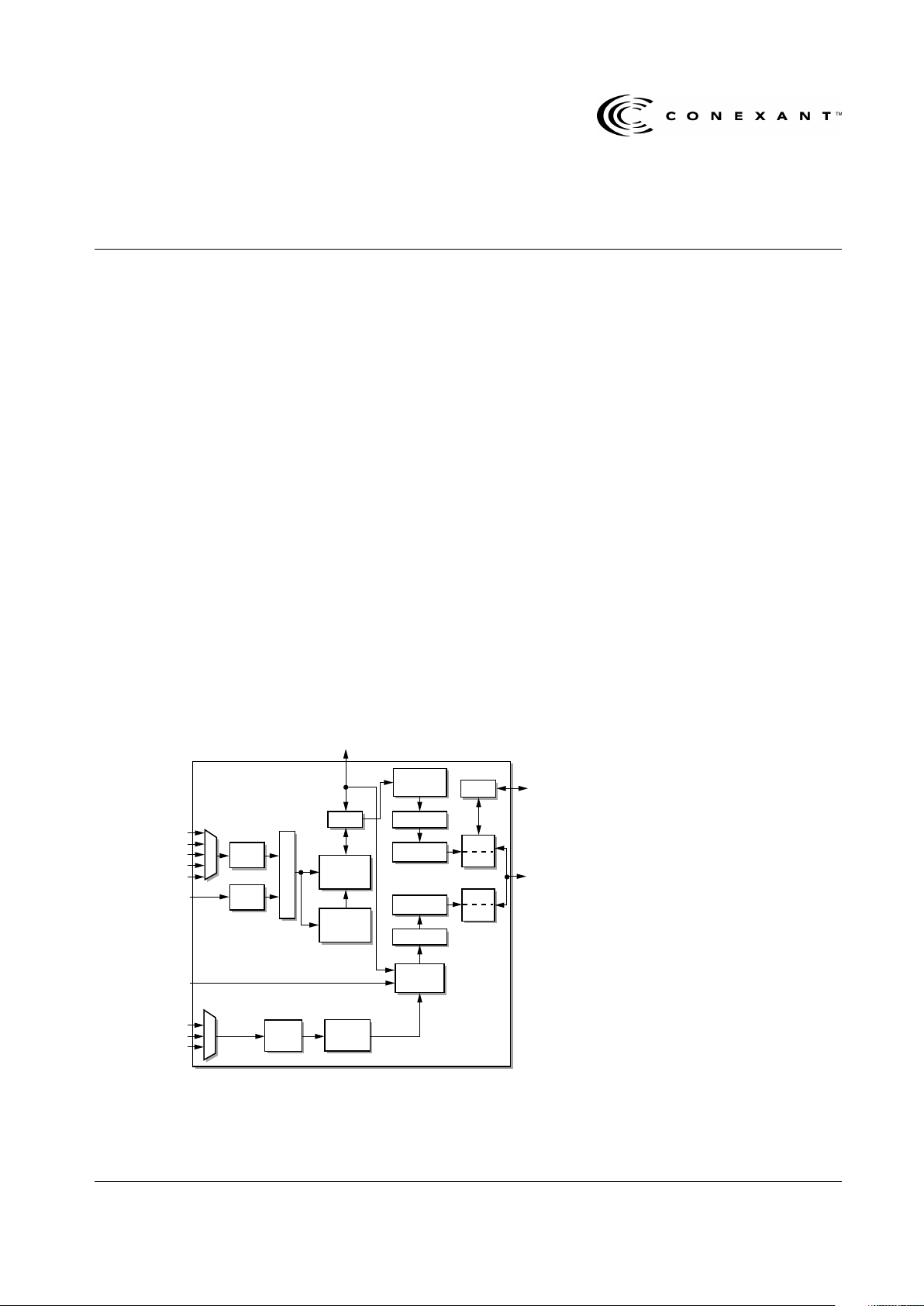
Functional Block Diagram
40 MHz
ADC
40 MHz
ADC
PCI I/F
Composite 1
PCI
Bus
S-Video (C)
TV
FM
Composite 2
Composite S-Video (Y)
Mic
High BW
Audio
ADC
Input
Gain
Control
Ultralock™
and Clock
Generation
Video
Decode
and Scaling
I
2
C
GPIO
Composite 3
Composite 4
GPIO and Digital/Video Port
3:1 MUX
Target
Initiator
Target
Initiator
Audio
Stream
Format
Audio FIFO
DMA
Controller
DMA
Controller
Video FIFO
Pixel
Format
Conversion
879A_001
I2S (dig. audio)
Decimation LPF
Distinguishing Features
• NTSC/PAL/SECAM video decoding
• Supports capture resolutions up to 768 x 576 (full
PAL)
• On-chip PCI bus mastering and bridge
functionality
• Supports HDTV/audio/MPEG2 transport data
across PCI bus
• High-speed serial port support MPEG transport
stream up to rates of 40 Mbps
• High-speed parallel port supports MPEG transport
streams up to 20 Mbps
• Flexible 24-bit wide GPIO
• CCIR656 interface
• Interfaces to a Digital TV data stream from a VSB
or OFDM demodulator
• Multiple YCrCb and RGB pixel formats and YUV
planar formats supported on output
• Selectable pixel density: 8, 16, 24, and 32 bits per
pixel
• Performs complex clipping of video source and
VGA video overlay
• Permits different program control and color
space/scaling for even and odd fields
• Executes Windows 98 “Scatter and Gather”
• Integrates advanced chroma and luma comb
filters/scalers
• Image scaleable in X and Y direction
• Y/C, 6-tap luma/2-tap chroma polyphase filter
• Receives Digital audio via I2S serial port
• Includes VBI data capture (closed captioning,
teletext, and Intercast data decoding)
• 100% PCI Rev. 2.2 compliant
• PC 98/PC 99 compliant
• WHQL-certifiable
• Accepts Mono audio input
• Packaged in compact 128-pin plastic QFP
Fusion 878A Specific Features
• Full stereo decoding for both TV audio (BTSC) and
FM radio
• Enhanced GPIO/I
2
S
• ACPI support
• Byte alignment
• Vital product data
• High speed serial port
• High speed parallel port
Applications
• PC television
• Digital television
• Digital VCR
• Desktop video phone
• Still frame capture
• VBI data service capture
Page 2

100600B Conexant
Information provided by Conexant Systems, Inc. (Conexant) is believed to be accurate and reliable. However, no responsibility is
assumed by Conexant for its use, nor any infringement of patents, copyrights, or other rights of third parties which may result from its
use. No license is granted by implication or otherwise under any patent rights or copyrights of Conexant other than for circuitry
embodied in Conexant products. Conexant reserves the right to change circuitry at any time without notice. This document is subject
to change without notice.
Conexant products are not designed or intended for use in life support appliances, devices, or systems where malfunction of a
Conexant product can reasonably be expected to result in personal injury or death. Conexant customers using or selling Conexant
products for use in such applications do so at their own risk and agree to fully indemnify Conexant for any damages resulting from
such improper use or sale.
Conexant, the Conexant symbol and “What’s Next in Communications Technologies” are trademarks of Conexant Systems, Inc.
Product names or services listed in this publication are for identification purposes only, and may be trademarks or registered
trademarks of third parties. All other marks mentioned herein are the property of their respective owners.
© 1999 Conexant Systems, Inc.
Printed in U.S.A.
All Rights Reserved
Reader Response: Conexant strives to produce quality documentation and welcomes your feedback. Please send
comments and suggestions to conexant.tech.pubs@conexant.com. For technical questions, contact your local
Conexant sales office or field applications engineer.
Ordering Information
Related Documents
Fusion Technical Reference Manual
Fusion Programmers Guide
Model Number Package Operating Temperature
Fusion 878A 128-pin PQFP 0 °C to + 70 °C
Page 3

100600B Conexant iii
Table of Contents
List of Figures . . . . . . . . . . . . . . . . . . . . . . . . . . . . . . . . . . . . . . . . . . . . . . . . . . . . . . . . . . . . . . . . . . . . . . . . . xi
List of Tables . . . . . . . . . . . . . . . . . . . . . . . . . . . . . . . . . . . . . . . . . . . . . . . . . . . . . . . . . . . . . . . . . . . . . . . . . xiii
1.0 Product Overview. . . . . . . . . . . . . . . . . . . . . . . . . . . . . . . . . . . . . . . . . . . . . . . . . . . . . . . . . . . . . . . 1-1
1.1 Functional Overview . . . . . . . . . . . . . . . . . . . . . . . . . . . . . . . . . . . . . . . . . . . . . . . . . . . . . . . . . 1-1
1.2 Detailed Features . . . . . . . . . . . . . . . . . . . . . . . . . . . . . . . . . . . . . . . . . . . . . . . . . . . . . . . . . . . 1-4
1.2.1 Video Capture . . . . . . . . . . . . . . . . . . . . . . . . . . . . . . . . . . . . . . . . . . . . . . . . . . . . . . . . 1-4
1.2.2 Audio Capture . . . . . . . . . . . . . . . . . . . . . . . . . . . . . . . . . . . . . . . . . . . . . . . . . . . . . . . . 1-4
1.2.3 Analog Video and Digital Camera Capture . . . . . . . . . . . . . . . . . . . . . . . . . . . . . . . . . . . . 1-4
1.2.4 Intel Intercast™ Support. . . . . . . . . . . . . . . . . . . . . . . . . . . . . . . . . . . . . . . . . . . . . . . . . 1-4
1.2.5 Video DMA Channels . . . . . . . . . . . . . . . . . . . . . . . . . . . . . . . . . . . . . . . . . . . . . . . . . . . 1-5
1.2.6 Audio DMA Channels . . . . . . . . . . . . . . . . . . . . . . . . . . . . . . . . . . . . . . . . . . . . . . . . . . . 1-5
1.2.7 Data Transport Engine . . . . . . . . . . . . . . . . . . . . . . . . . . . . . . . . . . . . . . . . . . . . . . . . . . 1-5
1.2.8 PCI Bus Interface . . . . . . . . . . . . . . . . . . . . . . . . . . . . . . . . . . . . . . . . . . . . . . . . . . . . . . 1-6
1.2.9 UltraLock™ . . . . . . . . . . . . . . . . . . . . . . . . . . . . . . . . . . . . . . . . . . . . . . . . . . . . . . . . . . 1-6
1.2.10 Scaling and Cropping . . . . . . . . . . . . . . . . . . . . . . . . . . . . . . . . . . . . . . . . . . . . . . . . . . . 1-6
1.2.11 Input Interface . . . . . . . . . . . . . . . . . . . . . . . . . . . . . . . . . . . . . . . . . . . . . . . . . . . . . . . . 1-6
1.2.12 GPIO Port . . . . . . . . . . . . . . . . . . . . . . . . . . . . . . . . . . . . . . . . . . . . . . . . . . . . . . . . . . . 1-7
1.2.13 Vertical Blanking Interval Data Capture . . . . . . . . . . . . . . . . . . . . . . . . . . . . . . . . . . . . . . 1-7
1.2.14 I2C Interface. . . . . . . . . . . . . . . . . . . . . . . . . . . . . . . . . . . . . . . . . . . . . . . . . . . . . . . . . . 1-7
1.2.15 HDTV Support . . . . . . . . . . . . . . . . . . . . . . . . . . . . . . . . . . . . . . . . . . . . . . . . . . . . . . . . 1-7
1.3 Pin Descriptions . . . . . . . . . . . . . . . . . . . . . . . . . . . . . . . . . . . . . . . . . . . . . . . . . . . . . . . . . . . . 1-8
2.0 Functional Description . . . . . . . . . . . . . . . . . . . . . . . . . . . . . . . . . . . . . . . . . . . . . . . . . . . . . . . . . . 2-1
2.1 UltraLockTM Functionality . . . . . . . . . . . . . . . . . . . . . . . . . . . . . . . . . . . . . . . . . . . . . . . . . . . . . 2-1
2.1.1 The Challenge . . . . . . . . . . . . . . . . . . . . . . . . . . . . . . . . . . . . . . . . . . . . . . . . . . . . . . . . 2-1
2.1.2 Operating Principles of UltraLock . . . . . . . . . . . . . . . . . . . . . . . . . . . . . . . . . . . . . . . . . . 2-1
2.2 Composite Video Input Formats . . . . . . . . . . . . . . . . . . . . . . . . . . . . . . . . . . . . . . . . . . . . . . . . 2-3
2.3 Y/C Separation and Chroma Demodulation . . . . . . . . . . . . . . . . . . . . . . . . . . . . . . . . . . . . . . . . 2-4
Page 4

Table of Contents Fusion 878A
PCI Video Decoder
iv Conexant 100600B
2.4 Video Scaling, Cropping, and Temporal Decimation . . . . . . . . . . . . . . . . . . . . . . . . . . . . . . . . . 2-7
2.4.1 Down-Scaling . . . . . . . . . . . . . . . . . . . . . . . . . . . . . . . . . . . . . . . . . . . . . . . . . . . . . . . . 2-7
2.4.1.1 Horizontal and Vertical Scaling . . . . . . . . . . . . . . . . . . . . . . . . . . . . . . . . . . . 2-7
2.4.1.2 Field Aligned Vertical Scaling . . . . . . . . . . . . . . . . . . . . . . . . . . . . . . . . . . . . . 2-7
2.4.1.3 Luminance Scaling . . . . . . . . . . . . . . . . . . . . . . . . . . . . . . . . . . . . . . . . . . . . 2-7
2.4.1.4 Peaking . . . . . . . . . . . . . . . . . . . . . . . . . . . . . . . . . . . . . . . . . . . . . . . . . . . 2-10
2.4.1.5 Chrominance Scaling . . . . . . . . . . . . . . . . . . . . . . . . . . . . . . . . . . . . . . . . . 2-13
2.4.1.6 Scaling Registers . . . . . . . . . . . . . . . . . . . . . . . . . . . . . . . . . . . . . . . . . . . . 2-13
2.4.2 Image Cropping . . . . . . . . . . . . . . . . . . . . . . . . . . . . . . . . . . . . . . . . . . . . . . . . . . . . . . 2-16
2.4.2.1 Cropping Registers . . . . . . . . . . . . . . . . . . . . . . . . . . . . . . . . . . . . . . . . . . . 2-18
2.4.3 Temporal Decimation . . . . . . . . . . . . . . . . . . . . . . . . . . . . . . . . . . . . . . . . . . . . . . . . . . 2-19
2.5 Video Adjustments . . . . . . . . . . . . . . . . . . . . . . . . . . . . . . . . . . . . . . . . . . . . . . . . . . . . . . . . . 2-21
2.5.1 The Hue Adjust Register . . . . . . . . . . . . . . . . . . . . . . . . . . . . . . . . . . . . . . . . . . . . . . . . 2-21
2.5.2 The Contrast Adjust Register . . . . . . . . . . . . . . . . . . . . . . . . . . . . . . . . . . . . . . . . . . . . 2-21
2.5.3 The Saturation Adjust Registers . . . . . . . . . . . . . . . . . . . . . . . . . . . . . . . . . . . . . . . . . . 2-21
2.5.4 The Brightness Register . . . . . . . . . . . . . . . . . . . . . . . . . . . . . . . . . . . . . . . . . . . . . . . . 2-21
2.6 Automatic Chrominance Gain Control . . . . . . . . . . . . . . . . . . . . . . . . . . . . . . . . . . . . . . . . . . . 2-22
2.7 Low Color Detection and Removal . . . . . . . . . . . . . . . . . . . . . . . . . . . . . . . . . . . . . . . . . . . . . 2-22
2.8 Coring . . . . . . . . . . . . . . . . . . . . . . . . . . . . . . . . . . . . . . . . . . . . . . . . . . . . . . . . . . . . . . . . . . . 2-23
2.9 VBI Data Output Interface . . . . . . . . . . . . . . . . . . . . . . . . . . . . . . . . . . . . . . . . . . . . . . . . . . . . 2-24
2.9.1 VBI Line Output Mode . . . . . . . . . . . . . . . . . . . . . . . . . . . . . . . . . . . . . . . . . . . . . . . . . 2-25
2.10 Video Data Format Conversion . . . . . . . . . . . . . . . . . . . . . . . . . . . . . . . . . . . . . . . . . . . . . . . . 2-27
2.10.1 Pixel Data Path. . . . . . . . . . . . . . . . . . . . . . . . . . . . . . . . . . . . . . . . . . . . . . . . . . . . . . . 2-27
2.10.2 Video Control Code Status Data . . . . . . . . . . . . . . . . . . . . . . . . . . . . . . . . . . . . . . . . . . 2-27
2.10.3 YCrCb to RGB Conversion . . . . . . . . . . . . . . . . . . . . . . . . . . . . . . . . . . . . . . . . . . . . . . 2-30
2.10.4 Gamma Correction Removal. . . . . . . . . . . . . . . . . . . . . . . . . . . . . . . . . . . . . . . . . . . . . 2-30
2.10.5 YCrCb Sub-sampling . . . . . . . . . . . . . . . . . . . . . . . . . . . . . . . . . . . . . . . . . . . . . . . . . . 2-30
2.10.6 Byte Swapping. . . . . . . . . . . . . . . . . . . . . . . . . . . . . . . . . . . . . . . . . . . . . . . . . . . . . . . 2-31
2.11 Video and Control Data FIFO . . . . . . . . . . . . . . . . . . . . . . . . . . . . . . . . . . . . . . . . . . . . . . . . . . 2-32
2.11.1 Logical Organization. . . . . . . . . . . . . . . . . . . . . . . . . . . . . . . . . . . . . . . . . . . . . . . . . . . 2-32
2.11.2 FIFO Data Interface. . . . . . . . . . . . . . . . . . . . . . . . . . . . . . . . . . . . . . . . . . . . . . . . . . . . 2-33
2.11.3 Physical Implementation . . . . . . . . . . . . . . . . . . . . . . . . . . . . . . . . . . . . . . . . . . . . . . . 2-34
2.11.4 FIFO Input/Output Rates . . . . . . . . . . . . . . . . . . . . . . . . . . . . . . . . . . . . . . . . . . . . . . . . 2-34
2.12 DMA Controller . . . . . . . . . . . . . . . . . . . . . . . . . . . . . . . . . . . . . . . . . . . . . . . . . . . . . . . . . . . . 2-36
2.12.1 Target Memory. . . . . . . . . . . . . . . . . . . . . . . . . . . . . . . . . . . . . . . . . . . . . . . . . . . . . . . 2-37
2.12.2 RISC Program Setup and Synchronization. . . . . . . . . . . . . . . . . . . . . . . . . . . . . . . . . . . 2-37
2.12.3 RISC Instructions. . . . . . . . . . . . . . . . . . . . . . . . . . . . . . . . . . . . . . . . . . . . . . . . . . . . . 2-38
2.12.4 Complex Clipping. . . . . . . . . . . . . . . . . . . . . . . . . . . . . . . . . . . . . . . . . . . . . . . . . . . . . 2-43
2.12.5 Executing Instructions . . . . . . . . . . . . . . . . . . . . . . . . . . . . . . . . . . . . . . . . . . . . . . . . . 2-44
2.12.6 FIFO Overrun Conditions. . . . . . . . . . . . . . . . . . . . . . . . . . . . . . . . . . . . . . . . . . . . . . . . 2-45
2.12.7 FIFO Data Stream Resynchronization . . . . . . . . . . . . . . . . . . . . . . . . . . . . . . . . . . . . . . 2-46
2.13 Byte Alignment . . . . . . . . . . . . . . . . . . . . . . . . . . . . . . . . . . . . . . . . . . . . . . . . . . . . . . . . . . . . 2-47
Page 5

Fusion 878A Table of Contents
PCI Video Decoder
100600B Conexant v
2.14 Multifunction Arbiter . . . . . . . . . . . . . . . . . . . . . . . . . . . . . . . . . . . . . . . . . . . . . . . . . . . . . . . . 2-48
2.14.1 Normal PCI Mode. . . . . . . . . . . . . . . . . . . . . . . . . . . . . . . . . . . . . . . . . . . . . . . . . . . . . 2-48
2.14.2 430FX Compatibility Mode . . . . . . . . . . . . . . . . . . . . . . . . . . . . . . . . . . . . . . . . . . . . . . 2-48
2.14.3 Interfacing with Non-PCI 2.1 Compliant Core Logic . . . . . . . . . . . . . . . . . . . . . . . . . . . . 2-49
2.15 Audio A/D . . . . . . . . . . . . . . . . . . . . . . . . . . . . . . . . . . . . . . . . . . . . . . . . . . . . . . . . . . . . . . . . 2-50
2.15.1 Muxing and Anti-aliasing Filtering. . . . . . . . . . . . . . . . . . . . . . . . . . . . . . . . . . . . . . . . . 2-50
2.15.2 Input Gain Control . . . . . . . . . . . . . . . . . . . . . . . . . . . . . . . . . . . . . . . . . . . . . . . . . . . . 2-50
2.16 High Speed Serial Interface Mode. . . . . . . . . . . . . . . . . . . . . . . . . . . . . . . . . . . . . . . . . . . . . . 2-52
2.17 Asynchronous Data Parallel Mode: Raw Data Capture. . . . . . . . . . . . . . . . . . . . . . . . . . . . . . . 2-53
2.18 Digital Audio Packetizer . . . . . . . . . . . . . . . . . . . . . . . . . . . . . . . . . . . . . . . . . . . . . . . . . . . . . 2-54
2.18.1 Audio FIFO Memory and Status Codes . . . . . . . . . . . . . . . . . . . . . . . . . . . . . . . . . . . . . 2-54
2.18.2 PCI Bus Latency Tolerance for Audio Buffer. . . . . . . . . . . . . . . . . . . . . . . . . . . . . . . . . . 2-54
2.18.3 FIFO Interface . . . . . . . . . . . . . . . . . . . . . . . . . . . . . . . . . . . . . . . . . . . . . . . . . . . . . . . 2-55
2.18.4 Audio Packets and Data Capture . . . . . . . . . . . . . . . . . . . . . . . . . . . . . . . . . . . . . . . . . . 2-56
2.18.5 Digital Audio Input . . . . . . . . . . . . . . . . . . . . . . . . . . . . . . . . . . . . . . . . . . . . . . . . . . . . 2-57
2.18.5.1 Digital Audio Input Mode. . . . . . . . . . . . . . . . . . . . . . . . . . . . . . . . . . . . . . . 2-57
2.18.6 Data Packet Mode . . . . . . . . . . . . . . . . . . . . . . . . . . . . . . . . . . . . . . . . . . . . . . . . . . . . 2-58
2.18.7 Audio Data Formats . . . . . . . . . . . . . . . . . . . . . . . . . . . . . . . . . . . . . . . . . . . . . . . . . . . 2-59
2.18.8 Audio Dropout Detection . . . . . . . . . . . . . . . . . . . . . . . . . . . . . . . . . . . . . . . . . . . . . . . 2-59
2.19 Digital Television Support . . . . . . . . . . . . . . . . . . . . . . . . . . . . . . . . . . . . . . . . . . . . . . . . . . . . 2-60
3.0 Electrical Interfaces . . . . . . . . . . . . . . . . . . . . . . . . . . . . . . . . . . . . . . . . . . . . . . . . . . . . . . . . . . . . 3-1
3.1 Input Interface. . . . . . . . . . . . . . . . . . . . . . . . . . . . . . . . . . . . . . . . . . . . . . . . . . . . . . . . . . . . . . 3-1
3.1.1 Analog Signal Selection . . . . . . . . . . . . . . . . . . . . . . . . . . . . . . . . . . . . . . . . . . . . . . . . . 3-1
3.1.2 Multiplexer Considerations . . . . . . . . . . . . . . . . . . . . . . . . . . . . . . . . . . . . . . . . . . . . . . . 3-2
3.1.3 Flash A/D Converters . . . . . . . . . . . . . . . . . . . . . . . . . . . . . . . . . . . . . . . . . . . . . . . . . . . 3-3
3.1.4 A/D Clamping. . . . . . . . . . . . . . . . . . . . . . . . . . . . . . . . . . . . . . . . . . . . . . . . . . . . . . . . . 3-3
3.1.5 Power-up Operation . . . . . . . . . . . . . . . . . . . . . . . . . . . . . . . . . . . . . . . . . . . . . . . . . . . . 3-3
3.1.6 Automatic Gain Controls. . . . . . . . . . . . . . . . . . . . . . . . . . . . . . . . . . . . . . . . . . . . . . . . . 3-3
3.1.7 Crystal Inputs and Clock Generation . . . . . . . . . . . . . . . . . . . . . . . . . . . . . . . . . . . . . . . . 3-3
3.1.8 2X Oversampling and Input Filtering . . . . . . . . . . . . . . . . . . . . . . . . . . . . . . . . . . . . . . . . 3-6
3.2 PCI Bus Interface . . . . . . . . . . . . . . . . . . . . . . . . . . . . . . . . . . . . . . . . . . . . . . . . . . . . . . . . . . . 3-8
3.3 General Purpose I/O Port . . . . . . . . . . . . . . . . . . . . . . . . . . . . . . . . . . . . . . . . . . . . . . . . . . . . 3-10
3.3.1 GPIO Pin Architecture. . . . . . . . . . . . . . . . . . . . . . . . . . . . . . . . . . . . . . . . . . . . . . . . . . 3-10
3.3.2 GPIO Modes in Fusion 878A. . . . . . . . . . . . . . . . . . . . . . . . . . . . . . . . . . . . . . . . . . . . . 3-10
3.3.3 GPIO Normal Mode . . . . . . . . . . . . . . . . . . . . . . . . . . . . . . . . . . . . . . . . . . . . . . . . . . . 3-10
3.3.4 SPI Input Mode . . . . . . . . . . . . . . . . . . . . . . . . . . . . . . . . . . . . . . . . . . . . . . . . . . . . . . 3-12
3.3.5 SPI Output Mode . . . . . . . . . . . . . . . . . . . . . . . . . . . . . . . . . . . . . . . . . . . . . . . . . . . . . 3-13
3.3.6 GPIO SPI Mode Timing Parameters. . . . . . . . . . . . . . . . . . . . . . . . . . . . . . . . . . . . . . . . 3-17
3.3.7 Digital Video Input Mode . . . . . . . . . . . . . . . . . . . . . . . . . . . . . . . . . . . . . . . . . . . . . . . 3-18
3.3.7.1 CCIR656 . . . . . . . . . . . . . . . . . . . . . . . . . . . . . . . . . . . . . . . . . . . . . . . . . . . 3-18
3.3.7.2 Modified SMPTE-125 . . . . . . . . . . . . . . . . . . . . . . . . . . . . . . . . . . . . . . . . . 3-19
3.3.8 GPIO Timing Diagram for SPI and Digital Video Input Modes . . . . . . . . . . . . . . . . . . . . . 3-20
3.4 I2C Interface . . . . . . . . . . . . . . . . . . . . . . . . . . . . . . . . . . . . . . . . . . . . . . . . . . . . . . . . . . . . . . 3-21
Page 6

Table of Contents Fusion 878A
PCI Video Decoder
vi Conexant 100600B
3.5 I2C Serial EEPROM Interface. . . . . . . . . . . . . . . . . . . . . . . . . . . . . . . . . . . . . . . . . . . . . . . . . . 3-23
3.5.1 EEPROM Address Mapping. . . . . . . . . . . . . . . . . . . . . . . . . . . . . . . . . . . . . . . . . . . . . . 3-23
3.5.2 Subsystem Vendor ID. . . . . . . . . . . . . . . . . . . . . . . . . . . . . . . . . . . . . . . . . . . . . . . . . . 3-24
3.5.2.1 EEPROM Upload at PCI Reset . . . . . . . . . . . . . . . . . . . . . . . . . . . . . . . . . . . 3-24
3.5.2.2 Register Load from BIOS. . . . . . . . . . . . . . . . . . . . . . . . . . . . . . . . . . . . . . . 3-24
3.5.2.3 Programming and Write-Protect . . . . . . . . . . . . . . . . . . . . . . . . . . . . . . . . . 3-25
3.5.3 Vital Product Data . . . . . . . . . . . . . . . . . . . . . . . . . . . . . . . . . . . . . . . . . . . . . . . . . . . . 3-25
3.5.3.1 Vital Product Data EEPROM Addressing. . . . . . . . . . . . . . . . . . . . . . . . . . . . 3-25
3.5.3.2 Vital Product Data Read Sequence . . . . . . . . . . . . . . . . . . . . . . . . . . . . . . . . 3-26
3.5.3.3 Vital Product Data Write Sequence. . . . . . . . . . . . . . . . . . . . . . . . . . . . . . . . 3-26
3.6 Power Management Interface . . . . . . . . . . . . . . . . . . . . . . . . . . . . . . . . . . . . . . . . . . . . . . . . . 3-28
3.6.1 PME# . . . . . . . . . . . . . . . . . . . . . . . . . . . . . . . . . . . . . . . . . . . . . . . . . . . . . . . . . . . . . 3-28
3.6.2 D3 Power States . . . . . . . . . . . . . . . . . . . . . . . . . . . . . . . . . . . . . . . . . . . . . . . . . . . . . 3-28
3.7 JTAG Interface. . . . . . . . . . . . . . . . . . . . . . . . . . . . . . . . . . . . . . . . . . . . . . . . . . . . . . . . . . . . . 3-29
3.7.1 Need for Functional Verification . . . . . . . . . . . . . . . . . . . . . . . . . . . . . . . . . . . . . . . . . . 3-29
3.7.2 JTAG Approach to Testability . . . . . . . . . . . . . . . . . . . . . . . . . . . . . . . . . . . . . . . . . . . . 3-29
3.7.3 Optional Device ID Register . . . . . . . . . . . . . . . . . . . . . . . . . . . . . . . . . . . . . . . . . . . . . 3-30
3.7.4 Verification with the TAP Controller . . . . . . . . . . . . . . . . . . . . . . . . . . . . . . . . . . . . . . . . 3-30
4.0 PC Board Layout Considerations . . . . . . . . . . . . . . . . . . . . . . . . . . . . . . . . . . . . . . . . . . . . . . . . . 4-1
4.1 Layout Considerations . . . . . . . . . . . . . . . . . . . . . . . . . . . . . . . . . . . . . . . . . . . . . . . . . . . . . . . 4-1
4.1.1 Capacitors . . . . . . . . . . . . . . . . . . . . . . . . . . . . . . . . . . . . . . . . . . . . . . . . . . . . . . . . . . . 4-1
4.1.2 Components . . . . . . . . . . . . . . . . . . . . . . . . . . . . . . . . . . . . . . . . . . . . . . . . . . . . . . . . . 4-2
4.2 Split Planes and Voltage Regulators . . . . . . . . . . . . . . . . . . . . . . . . . . . . . . . . . . . . . . . . . . . . . 4-3
4.3 Latchup Avoidance . . . . . . . . . . . . . . . . . . . . . . . . . . . . . . . . . . . . . . . . . . . . . . . . . . . . . . . . . . 4-4
5.0 Control Register Definitions-Function 0. . . . . . . . . . . . . . . . . . . . . . . . . . . . . . . . . . . . . . . . . . . 5-1
5.1 PCI Configuration Space . . . . . . . . . . . . . . . . . . . . . . . . . . . . . . . . . . . . . . . . . . . . . . . . . . . . . . 5-1
5.2 PCI Configuration Registers (Header) . . . . . . . . . . . . . . . . . . . . . . . . . . . . . . . . . . . . . . . . . . . . 5-3
0x00—Vendor and Device ID Register . . . . . . . . . . . . . . . . . . . . . . . . . . . . . . . . . . . 5-3
0x04—Command and Status Register . . . . . . . . . . . . . . . . . . . . . . . . . . . . . . . . . . . 5-3
0x08—Revision ID and Class Code Register . . . . . . . . . . . . . . . . . . . . . . . . . . . . . . 5-4
0x0C—Header Type, Latency Timer Register . . . . . . . . . . . . . . . . . . . . . . . . . . . . . . 5-4
0x10—Base Address 0 Register . . . . . . . . . . . . . . . . . . . . . . . . . . . . . . . . . . . . . . . 5-4
0x2C—Subsystem ID and Subsystem Vendor ID Register . . . . . . . . . . . . . . . . . . . . 5-4
0x3C—Interrupt Line, Interrupt Pin, Min_Gnt, Max_Lat Register. . . . . . . . . . . . . . . . 5-5
0x34—Capabilities Pointer Register. . . . . . . . . . . . . . . . . . . . . . . . . . . . . . . . . . . . . 5-5
0x40—Device Control Register . . . . . . . . . . . . . . . . . . . . . . . . . . . . . . . . . . . . . . . . 5-5
0x44—VPD Capability Register . . . . . . . . . . . . . . . . . . . . . . . . . . . . . . . . . . . . . . . . 5-6
0x48—VPD Data Register . . . . . . . . . . . . . . . . . . . . . . . . . . . . . . . . . . . . . . . . . . . . 5-6
0x4C—Power Management Capability Register . . . . . . . . . . . . . . . . . . . . . . . . . . . . 5-6
0x50—Power Management Support Registers . . . . . . . . . . . . . . . . . . . . . . . . . . . . . 5-7
5.3 Local Registers (Memory Mapped) . . . . . . . . . . . . . . . . . . . . . . . . . . . . . . . . . . . . . . . . . . . . . . 5-8
0x000—Device Status Register (DSTATUS). . . . . . . . . . . . . . . . . . . . . . . . . . . . . . . 5-9
0x004—Input Format Register (IFORM) . . . . . . . . . . . . . . . . . . . . . . . . . . . . . . . . 5-10
0x008—Temporal Decimation Register (TDEC) . . . . . . . . . . . . . . . . . . . . . . . . . . . 5-10
Page 7

Fusion 878A Table of Contents
PCI Video Decoder
100600B Conexant vii
MSB Cropping Register) . . . . . . . . . . . . . . . . . . . . . . . . . . . . . . . . . . . . . . . . . . . . 5-11
0x00C—Even Field (E_CROP)
0x08C—Odd Field (O_CROP)
. . . . . . . . . . . . . . . . . . . . . . . . . . . . . . . . . . . 5-11
Vertical Delay Register, Lower Byte . . . . . . . . . . . . . . . . . . . . . . . . . . . . . . . . . . . . 5-11
0x090—Even Field (E_VDELAY_LO)
0x010—Odd Field (O_VDELAY_LO)
. . . . . . . . . . . . . . . . . . . . . . . . . . . . . . . 5-11
Vertical Active Register, Lower Byte. . . . . . . . . . . . . . . . . . . . . . . . . . . . . . . . . . . . 5-11
0x014—Even Field (E_VACTIVE_LO)
0x094—Odd Field (O_VACTIVE_LO)
. . . . . . . . . . . . . . . . . . . . . . . . . . . . . . 5-11
Horizontal Delay Register, Lower Byte . . . . . . . . . . . . . . . . . . . . . . . . . . . . . . . . . . 5-12
0x018—Even Field (E_DELAY_LO)
0x098—Odd Field (O_DELAY_LO)
. . . . . . . . . . . . . . . . . . . . . . . . . . . . . . . . 5-12
Horizontal Active Register, Lower Byte. . . . . . . . . . . . . . . . . . . . . . . . . . . . . . . . . . 5-12
0x01C—Even Field (E_HACTIVE_LO)
0x09C—Odd Field (O_HACTIVE_LO)
. . . . . . . . . . . . . . . . . . . . . . . . . . . . . . 5-12
Horizontal Scaling Register, Upper Byte. . . . . . . . . . . . . . . . . . . . . . . . . . . . . . . . . 5-12
0x020—Even Field (E_HSCALE_HI)
0x0A0—Odd Field (O_HSCALE_HI)
. . . . . . . . . . . . . . . . . . . . . . . . . . . . . . . 5-12
Horizontal Scaling Register, Lower Byte. . . . . . . . . . . . . . . . . . . . . . . . . . . . . . . . . 5-12
0x024—Even Field (E_HSCALE_LO)
0x0A4—Odd Field (O_HSCALE_LO)
. . . . . . . . . . . . . . . . . . . . . . . . . . . . . . 5-12
0x028—Brightness Control Register (BRIGHT). . . . . . . . . . . . . . . . . . . . . . . . . . . 5-13
Miscellaneous Control Register . . . . . . . . . . . . . . . . . . . . . . . . . . . . . . . . . . . . . . . 5-14
0x02C—Even Field (E_CONTROL)
0x0AC—Odd Field (O_CONTROL)
. . . . . . . . . . . . . . . . . . . . . . . . . . . . . . . . 5-14
0x030—Luma Gain Register, Lower Byte (CONTRAST_LO) . . . . . . . . . . . . . . . . . . 5-15
0x034—Chroma (U) Gain Register, Lower Byte (SAT_U_LO) . . . . . . . . . . . . . . . . . 5-16
0x038—Chroma (V) Gain Register, Lower Byte (SAT_V_LO) . . . . . . . . . . . . . . . . . 5-17
0x03C—Hue Control Register (HUE). . . . . . . . . . . . . . . . . . . . . . . . . . . . . . . . . . . 5-18
SC Loop Control Register . . . . . . . . . . . . . . . . . . . . . . . . . . . . . . . . . . . . . . . . . . . 5-19
0x040—Even Field (E_SCLOOP)
0x0C0—Odd Field (O_SCLOOP)
. . . . . . . . . . . . . . . . . . . . . . . . . . . . . . . . . 5-19
0x044—White Crush Up Register (WC_UP). . . . . . . . . . . . . . . . . . . . . . . . . . . . . . 5-20
0x048—Output Format Register (OFORM). . . . . . . . . . . . . . . . . . . . . . . . . . . . . . . 5-20
Vertical Scaling Register, Upper Byte . . . . . . . . . . . . . . . . . . . . . . . . . . . . . . . . . . . 5-21
0x04C—Even Field (E_VSCALE_HI)
0x0CC—Odd Field (O_VSCALE_HI)
. . . . . . . . . . . . . . . . . . . . . . . . . . . . . . . 5-21
Vertical Scaling Register, Lower Byte. . . . . . . . . . . . . . . . . . . . . . . . . . . . . . . . . . . 5-21
0x050—Even Field (E_VSCALE_LO)
0x0D0—Odd Field (O_VSCALE_LO)
. . . . . . . . . . . . . . . . . . . . . . . . . . . . . . 5-21
0x054—Reserved . . . . . . . . . . . . . . . . . . . . . . . . . . . . . . . . . . . . . . . . . . . . . . . . . 5-21
0x5B—Audio Reset Register (ARESET) . . . . . . . . . . . . . . . . . . . . . . . . . . . . . . . . . 5-22
0x060—AGC Delay Register (ADELAY) . . . . . . . . . . . . . . . . . . . . . . . . . . . . . . . . . 5-22
0x064—Burst Delay Register (BDELAY) . . . . . . . . . . . . . . . . . . . . . . . . . . . . . . . . 5-22
0x068—ADC Interface Register (ADC) . . . . . . . . . . . . . . . . . . . . . . . . . . . . . . . . . 5-23
Video Timing Control Register . . . . . . . . . . . . . . . . . . . . . . . . . . . . . . . . . . . . . . . . 5-24
0x6C—Even Field (E_VTC)
0xEC—Odd Field (O_VTC)
. . . . . . . . . . . . . . . . . . . . . . . . . . . . . . . . . . . . . . 5-24
0x07C—Software Reset Register (SRESET). . . . . . . . . . . . . . . . . . . . . . . . . . . . . . 5-24
0x078—White Crush Down Register . . . . . . . . . . . . . . . . . . . . . . . . . . . . . . . . . . . 5-25
0x080—Timing Generator Load Byte (TGLB) . . . . . . . . . . . . . . . . . . . . . . . . . . . . . 5-25
0x084—Timing Generator Control (TGCTRL) Register . . . . . . . . . . . . . . . . . . . . . . 5-26
0x0B0—Total Line Count Register (VTOTAL_LO) . . . . . . . . . . . . . . . . . . . . . . . . . . 5-27
Page 8

Table of Contents Fusion 878A
PCI Video Decoder
viii Conexant 100600B
0x0B4—Total Line Count Register (VTOTAL_HI). . . . . . . . . . . . . . . . . . . . . . . . . . 5-27
0x0D4—Color Format Register (COLOR_FMT). . . . . . . . . . . . . . . . . . . . . . . . . . . . 5-28
0x0D8—Color Control Register (COLOR_CTL). . . . . . . . . . . . . . . . . . . . . . . . . . . . 5-29
0x0DC—Capture Control Register (CAP_CTL) . . . . . . . . . . . . . . . . . . . . . . . . . . . . 5-29
0x0E0—VBI Packet Size Register (VBI_PACK_SIZE) . . . . . . . . . . . . . . . . . . . . . . . 5-30
0x0E4—VBI Packet Size / Delay Register (VBI_PACK_DEL). . . . . . . . . . . . . . . . . . 5-30
0x0E8—Field Capture Counter Register (FCAP) . . . . . . . . . . . . . . . . . . . . . . . . . . . 5-30
0x0F0—PLL Reference Multiplier Register (PLL_F_LO) . . . . . . . . . . . . . . . . . . . . . 5-30
0x0F4—PLL Reference Multiplier Register (PLL_F_HI). . . . . . . . . . . . . . . . . . . . . . 5-30
0x0F8—Integer Register (PLL-XCI) . . . . . . . . . . . . . . . . . . . . . . . . . . . . . . . . . . . . 5-31
0x0FC—Digital Video Signal Interface Format (DVSIF) Register . . . . . . . . . . . . . . . 5-31
0x100—Interrupt Status Register (INT_STAT) . . . . . . . . . . . . . . . . . . . . . . . . . . . . 5-32
0x104—Interrupt Mask Register (INT_MASK) . . . . . . . . . . . . . . . . . . . . . . . . . . . . 5-33
0x10C—GPIO and DMA Control Register (GPIO_DMA_CTL) . . . . . . . . . . . . . . . . . 5-34
0x110—I2C Data/Control Register. . . . . . . . . . . . . . . . . . . . . . . . . . . . . . . . . . . . . 5-35
0x114—RISC Program Start Address Register (RISC_STRT_ADD) . . . . . . . . . . . . 5-36
0x118—GPIO Output Enable Control Register (GPIO_OUT_EN) . . . . . . . . . . . . . . . 5-36
0x120—RISC Program Counter Register (RISC_COUNT) . . . . . . . . . . . . . . . . . . . 5-36
0x200–0x2FF—GPIO Data I/O Register (GPIO_DATA) . . . . . . . . . . . . . . . . . . . . . . 5-36
6.0 Control Register Definitions–Function 1 . . . . . . . . . . . . . . . . . . . . . . . . . . . . . . . . . . . . . . . . . . 6-1
6.1 PCI Configuration Space . . . . . . . . . . . . . . . . . . . . . . . . . . . . . . . . . . . . . . . . . . . . . . . . . . . . . . 6-1
6.2 PCI Configuration Registers (Header) . . . . . . . . . . . . . . . . . . . . . . . . . . . . . . . . . . . . . . . . . . . . 6-3
0x00—Vendor and Device ID Register . . . . . . . . . . . . . . . . . . . . . . . . . . . . . . . . . . . 6-3
0x04—Command and Status Register . . . . . . . . . . . . . . . . . . . . . . . . . . . . . . . . . . . 6-3
0x08—Revision ID and Class Code Register . . . . . . . . . . . . . . . . . . . . . . . . . . . . . . 6-4
0x0C—Header Type Register. . . . . . . . . . . . . . . . . . . . . . . . . . . . . . . . . . . . . . . . . . 6-4
0x0C—Latency Timer Register . . . . . . . . . . . . . . . . . . . . . . . . . . . . . . . . . . . . . . . . 6-4
0x10—Base Address 0 Register . . . . . . . . . . . . . . . . . . . . . . . . . . . . . . . . . . . . . . . 6-4
0x2C—Subsystem ID and Subsystem Vendor ID Register . . . . . . . . . . . . . . . . . . . . 6-5
0x34—Capabilities Pointer Register. . . . . . . . . . . . . . . . . . . . . . . . . . . . . . . . . . . . . 6-5
0x3C—Interrupt Line, Interrupt Pin, Min_Gnt, Max_Lat Register. . . . . . . . . . . . . . . . 6-5
0x40—Device Control Register . . . . . . . . . . . . . . . . . . . . . . . . . . . . . . . . . . . . . . . . 6-6
0x44—VPD Capability Register . . . . . . . . . . . . . . . . . . . . . . . . . . . . . . . . . . . . . . . . 6-6
0x48—VPD Data Register . . . . . . . . . . . . . . . . . . . . . . . . . . . . . . . . . . . . . . . . . . . . 6-7
0x4C—Power Management Capability Register . . . . . . . . . . . . . . . . . . . . . . . . . . . . 6-7
0x50—Power Management Support Register. . . . . . . . . . . . . . . . . . . . . . . . . . . . . . 6-8
6.3 Local Registers (Memory Mapped) . . . . . . . . . . . . . . . . . . . . . . . . . . . . . . . . . . . . . . . . . . . . . . 6-9
0x100—Interrupt Status Register (INT_STAT) . . . . . . . . . . . . . . . . . . . . . . . . . . . 6-10
0x104—Interrupt Mask Register (INT_MASK). . . . . . . . . . . . . . . . . . . . . . . . . . . . 6-11
0x10C—Audio Control Register (GPIO_DMA_CTL) . . . . . . . . . . . . . . . . . . . . . . . . 6-11
0x110—Audio Packet Lengths Register. . . . . . . . . . . . . . . . . . . . . . . . . . . . . . . . . 6-13
0x114—RISC Program Start Address Register (RISC_STRT_ADD). . . . . . . . . . . . . 6-13
0x120—RISC Program Counter Register (RISC_COUNT) . . . . . . . . . . . . . . . . . . . . 6-13
7.0 Parametric Information . . . . . . . . . . . . . . . . . . . . . . . . . . . . . . . . . . . . . . . . . . . . . . . . . . . . . . . . . 7-1
7.1 DC Electrical Parameters . . . . . . . . . . . . . . . . . . . . . . . . . . . . . . . . . . . . . . . . . . . . . . . . . . . . . 7-1
7.2 AC Electrical Parameters . . . . . . . . . . . . . . . . . . . . . . . . . . . . . . . . . . . . . . . . . . . . . . . . . . . . . 7-4
7.3 Package Mechanical Drawing. . . . . . . . . . . . . . . . . . . . . . . . . . . . . . . . . . . . . . . . . . . . . . . . . . 7-6
Appendix A. Acronym List . . . . . . . . . . . . . . . . . . . . . . . . . . . . . . . . . . . . . . . . . . . . . . . . . . . . . . . . . . . . . A-1
Page 9

Fusion 878A List of Figures
PCI Video Decoder
100600B Conexant xi
List of Figures
Figure 1-1. Fusion 878A Detailed Block Diagram. . . . . . . . . . . . . . . . . . . . . . . . . . . . . . . . . . . . . . . . . .1-2
Figure 1-2. Fusion 878A Audio/Video Decoder and Scaler Block Diagram . . . . . . . . . . . . . . . . . . . . . . 1-3
Figure 1-3. Fusion 878A Pinout Diagram. . . . . . . . . . . . . . . . . . . . . . . . . . . . . . . . . . . . . . . . . . . . . . . . 1-8
Figure 2-1. UltraLock Behavior for NTSC Square Pixel Output . . . . . . . . . . . . . . . . . . . . . . . . . . . . . . . 2-2
Figure 2-2. Y/C Separation and Chroma Demodulation for Composite Video . . . . . . . . . . . . . . . . . . . . 2-4
Figure 2-3. Y/C Separation Filter Responses . . . . . . . . . . . . . . . . . . . . . . . . . . . . . . . . . . . . . . . . . . . . . 2-5
Figure 2-4. Filtering and Scaling . . . . . . . . . . . . . . . . . . . . . . . . . . . . . . . . . . . . . . . . . . . . . . . . . . . . . . 2-6
Figure 2-5. Optional Horizontal Luma Low-Pass Filter Responses . . . . . . . . . . . . . . . . . . . . . . . . . . . . 2-8
Figure 2-6. Combined Luma Notch, 2x Oversampling and Optional
Low-Pass Filter Response (NTSC) . . . . . . . . . . . . . . . . . . . . . . . . . . . . . . . . . . . . . . . . . . . 2-8
Figure 2-7. Combined Luma Notch, 2x Oversampling and Optional
Low-Pass Filter Response (PAL/SECAM) . . . . . . . . . . . . . . . . . . . . . . . . . . . . . . . . . . . . . . 2-9
Figure 2-8. Combined Luma Notch and 2x Oversampling Filter Response . . . . . . . . . . . . . . . . . . . . . . 2-9
Figure 2-9. Frequency Responses for the Four Optional Vertical Luma Low-Pass Filters . . . . . . . . . . 2-10
Figure 2-10. Peaking Filters. . . . . . . . . . . . . . . . . . . . . . . . . . . . . . . . . . . . . . . . . . . . . . . . . . . . . . . . . . 2-11
Figure 2-11. Luma Peaking Filters with 2x Oversampling Filter and Luma Notch . . . . . . . . . . . . . . . . . 2-12
Figure 2-12. Effect of the Cropping and Active Registers . . . . . . . . . . . . . . . . . . . . . . . . . . . . . . . . . . . 2-17
Figure 2-13. Regions of the Video Signal . . . . . . . . . . . . . . . . . . . . . . . . . . . . . . . . . . . . . . . . . . . . . . . 2-18
Figure 2-14. Coring Map . . . . . . . . . . . . . . . . . . . . . . . . . . . . . . . . . . . . . . . . . . . . . . . . . . . . . . . . . . . . 2-23
Figure 2-15. Regions of the NTSC Video Frame . . . . . . . . . . . . . . . . . . . . . . . . . . . . . . . . . . . . . . . . . . 2-24
Figure 2-16. Regions of the PAL Video Frame (Fields 1, 2, 5, and 6) . . . . . . . . . . . . . . . . . . . . . . . . . . 2-24
Figure 2-17. VBI Timing . . . . . . . . . . . . . . . . . . . . . . . . . . . . . . . . . . . . . . . . . . . . . . . . . . . . . . . . . . . . 2-25
Figure 2-18. VBI Section Block Diagram . . . . . . . . . . . . . . . . . . . . . . . . . . . . . . . . . . . . . . . . . . . . . . . . 2-26
Figure 2-19. Video Data Format Converter . . . . . . . . . . . . . . . . . . . . . . . . . . . . . . . . . . . . . . . . . . . . . . 2-28
Figure 2-20. Data FIFO Block Diagram. . . . . . . . . . . . . . . . . . . . . . . . . . . . . . . . . . . . . . . . . . . . . . . . . . 2-32
Figure 2-21. Audio/Video RISC Block Diagram . . . . . . . . . . . . . . . . . . . . . . . . . . . . . . . . . . . . . . . . . . .2-37
Figure 2-22. Example of Complex Clipping . . . . . . . . . . . . . . . . . . . . . . . . . . . . . . . . . . . . . . . . . . . . . . 2-44
Figure 2-23. Asynchronous Data Parallel Input Multiplexer Block. . . . . . . . . . . . . . . . . . . . . . . . . . . . . 2-53
Figure 2-24. FIFO Interface . . . . . . . . . . . . . . . . . . . . . . . . . . . . . . . . . . . . . . . . . . . . . . . . . . . . . . . . . . 2-55
Figure 2-25. Audio Input Timing . . . . . . . . . . . . . . . . . . . . . . . . . . . . . . . . . . . . . . . . . . . . . . . . . . . . . . 2-57
Figure 2-26. Data Packet Mode Timing . . . . . . . . . . . . . . . . . . . . . . . . . . . . . . . . . . . . . . . . . . . . . . . . . 2-58
Figure 2-27. Audio Data Path. . . . . . . . . . . . . . . . . . . . . . . . . . . . . . . . . . . . . . . . . . . . . . . . . . . . . . . . . 2-59
Figure 3-1. Typical External Circuitry. . . . . . . . . . . . . . . . . . . . . . . . . . . . . . . . . . . . . . . . . . . . . . . . . . . 3-2
Figure 3-2. Clock Options . . . . . . . . . . . . . . . . . . . . . . . . . . . . . . . . . . . . . . . . . . . . . . . . . . . . . . . . . . . 3-6
Figure 3-3. Luma and Chroma 2x Oversampling Filter . . . . . . . . . . . . . . . . . . . . . . . . . . . . . . . . . . . . . 3-7
Figure 3-4. PCI Video Block Diagram . . . . . . . . . . . . . . . . . . . . . . . . . . . . . . . . . . . . . . . . . . . . . . . . . . 3-9
Figure 3-5. PCI Audio Block Diagram . . . . . . . . . . . . . . . . . . . . . . . . . . . . . . . . . . . . . . . . . . . . . . . . . . 3-9
Figure 3-6. GPIO Pin Architecture . . . . . . . . . . . . . . . . . . . . . . . . . . . . . . . . . . . . . . . . . . . . . . . . . . . . 3-10
Figure 3-7. GPIO Normal Mode . . . . . . . . . . . . . . . . . . . . . . . . . . . . . . . . . . . . . . . . . . . . . . . . . . . . . . 3-11
Page 10

List of Figures Fusion 878A
PCI Video Decoder
xii Conexant 100600B
Figure 3-8. GPIO SPI Input Mode . . . . . . . . . . . . . . . . . . . . . . . . . . . . . . . . . . . . . . . . . . . . . . . . . . . . 3-12
Figure 3-9. GPIO SPI Output Mode . . . . . . . . . . . . . . . . . . . . . . . . . . . . . . . . . . . . . . . . . . . . . . . . . . . 3-13
Figure 3-10. Basic Timing Relationships for SPI Output Mode . . . . . . . . . . . . . . . . . . . . . . . . . . . . . . . 3-15
Figure 3-11. Video Timing in SPI Output Mode. . . . . . . . . . . . . . . . . . . . . . . . . . . . . . . . . . . . . . . . . . .3-16
Figure 3-12. CCIR 656 Interface to Digital Input Port . . . . . . . . . . . . . . . . . . . . . . . . . . . . . . . . . . . . . .3-19
Figure 3-13. GPIO Timing Diagram . . . . . . . . . . . . . . . . . . . . . . . . . . . . . . . . . . . . . . . . . . . . . . . . . . . . 3-20
Figure 3-14. The Relationship Between SCL and SDA. . . . . . . . . . . . . . . . . . . . . . . . . . . . . . . . . . . . . . 3-21
Figure 3-15. I
2
C Typical Protocol Diagram . . . . . . . . . . . . . . . . . . . . . . . . . . . . . . . . . . . . . . . . . . . . . . 3-22
Figure 3-16. Instruction Register. . . . . . . . . . . . . . . . . . . . . . . . . . . . . . . . . . . . . . . . . . . . . . . . . . . . . . 3-30
Figure 4-1. Optional Regulatory Circuitry . . . . . . . . . . . . . . . . . . . . . . . . . . . . . . . . . . . . . . . . . . . . . . . 4-4
Figure 5-1. Function 0 PCI Configuration Space Header . . . . . . . . . . . . . . . . . . . . . . . . . . . . . . . . . . . . 5-2
Figure 6-1. Function 1 PCI Configuration Space Header . . . . . . . . . . . . . . . . . . . . . . . . . . . . . . . . . . . . 6-2
Figure 7-1. Clock Timing Diagram. . . . . . . . . . . . . . . . . . . . . . . . . . . . . . . . . . . . . . . . . . . . . . . . . . . . . 7-4
Figure 7-2. JTAG Timing Diagram . . . . . . . . . . . . . . . . . . . . . . . . . . . . . . . . . . . . . . . . . . . . . . . . . . . . . 7-5
Figure 7-3. 128-pin PQFP Package Mechanical Drawing. . . . . . . . . . . . . . . . . . . . . . . . . . . . . . . . . . . . 7-6
Page 11

Fusion 878A List of Tables
PCI Video Decoder
100600B Conexant xiii
List of Tables
Table 1-1. Audio/Video Capture Product Family. . . . . . . . . . . . . . . . . . . . . . . . . . . . . . . . . . . . . . . . . . .1-1
Table 1-2. Pin Descriptions Grouped by Pin Function . . . . . . . . . . . . . . . . . . . . . . . . . . . . . . . . . . . . . . 1-9
Table 2-1. Video Input Formats Supported by the Fusion 878A. . . . . . . . . . . . . . . . . . . . . . . . . . . . . . . 2-3
Table 2-2. Register Values for Square Pixel Video Input Formats . . . . . . . . . . . . . . . . . . . . . . . . . . . . . 2-3
Table 2-3. Scaling Ratios for Popular Formats Using Frequency Values . . . . . . . . . . . . . . . . . . . . . . . 2-16
Table 2-4. Square Pixel Values. . . . . . . . . . . . . . . . . . . . . . . . . . . . . . . . . . . . . . . . . . . . . . . . . . . . . . . 2-18
Table 2-5. Color Formats . . . . . . . . . . . . . . . . . . . . . . . . . . . . . . . . . . . . . . . . . . . . . . . . . . . . . . . . . . . 2-29
Table 2-6. Byte Swapping Map . . . . . . . . . . . . . . . . . . . . . . . . . . . . . . . . . . . . . . . . . . . . . . . . . . . . . . 2-31
Table 2-7. Status Bits. . . . . . . . . . . . . . . . . . . . . . . . . . . . . . . . . . . . . . . . . . . . . . . . . . . . . . . . . . . . . . 2-33
Table 2-8. FIFO Full/Almost Full Counts . . . . . . . . . . . . . . . . . . . . . . . . . . . . . . . . . . . . . . . . . . . . . . . . 2-34
Table 2-9. Table of PCI Bus Access Latencies . . . . . . . . . . . . . . . . . . . . . . . . . . . . . . . . . . . . . . . . . . .2-35
Table 2-10. RISC Instructions . . . . . . . . . . . . . . . . . . . . . . . . . . . . . . . . . . . . . . . . . . . . . . . . . . . . . . . . 2-38
Table 2-11. Write 640 Pixels in RGB8 Mode . . . . . . . . . . . . . . . . . . . . . . . . . . . . . . . . . . . . . . . . . . . . . 2-47
Table 2-12. Gain Control . . . . . . . . . . . . . . . . . . . . . . . . . . . . . . . . . . . . . . . . . . . . . . . . . . . . . . . . . . . . 2-50
Table 2-13. Digital Audio Packetizer Programming Map . . . . . . . . . . . . . . . . . . . . . . . . . . . . . . . . . . . . 2-54
Table 2-14. Audio Data Formats. . . . . . . . . . . . . . . . . . . . . . . . . . . . . . . . . . . . . . . . . . . . . . . . . . . . . . . 2-59
Table 3-1. Recommended Crystals . . . . . . . . . . . . . . . . . . . . . . . . . . . . . . . . . . . . . . . . . . . . . . . . . . . . 3-5
Table 3-2. SPI Input GPIO Signals . . . . . . . . . . . . . . . . . . . . . . . . . . . . . . . . . . . . . . . . . . . . . . . . . . . . 3-12
Table 3-3. SPI GPIO Output Signals. . . . . . . . . . . . . . . . . . . . . . . . . . . . . . . . . . . . . . . . . . . . . . . . . . . 3-14
Table 3-4. GPIO SPI Mode Timing Parameters . . . . . . . . . . . . . . . . . . . . . . . . . . . . . . . . . . . . . . . . . . 3-17
Table 3-5. Pin Definition of GPIO Port When Using Digital Video-In Mode . . . . . . . . . . . . . . . . . . . . . 3-18
Table 3-6. External EEPROM Memory Map . . . . . . . . . . . . . . . . . . . . . . . . . . . . . . . . . . . . . . . . . . . . . 3-23
Table 3-7. EEPROM Upload Sequence . . . . . . . . . . . . . . . . . . . . . . . . . . . . . . . . . . . . . . . . . . . . . . . . .3-24
Table 3-8. VPD Read Sequence . . . . . . . . . . . . . . . . . . . . . . . . . . . . . . . . . . . . . . . . . . . . . . . . . . . . . . 3-26
Table 3-9. VPD Write Sequence . . . . . . . . . . . . . . . . . . . . . . . . . . . . . . . . . . . . . . . . . . . . . . . . . . . . . . 3-26
Table 3-10. Device Identification Register . . . . . . . . . . . . . . . . . . . . . . . . . . . . . . . . . . . . . . . . . . . . . . . 3-30
Table 4-1. Capacitor Location . . . . . . . . . . . . . . . . . . . . . . . . . . . . . . . . . . . . . . . . . . . . . . . . . . . . . . . . 4-1
Table 5-1. BRIGHT Parameters . . . . . . . . . . . . . . . . . . . . . . . . . . . . . . . . . . . . . . . . . . . . . . . . . . . . . . 5-13
Table 5-2. CONTRAST Parameters. . . . . . . . . . . . . . . . . . . . . . . . . . . . . . . . . . . . . . . . . . . . . . . . . . . . 5-15
Table 5-3. (SAT_U_MSB + SAT_U_LO) . . . . . . . . . . . . . . . . . . . . . . . . . . . . . . . . . . . . . . . . . . . . . . . .5-16
Table 5-4. SAT_V (SAT_V_MSB + SAT_V_LO). . . . . . . . . . . . . . . . . . . . . . . . . . . . . . . . . . . . . . . . . . . 5-17
Table 5-5. HUE Parameters . . . . . . . . . . . . . . . . . . . . . . . . . . . . . . . . . . . . . . . . . . . . . . . . . . . . . . . . . 5-18
Table 7-1. Recommended Operating Conditions . . . . . . . . . . . . . . . . . . . . . . . . . . . . . . . . . . . . . . . . . . 7-1
Table 7-2. Absolute Maximum Ratings . . . . . . . . . . . . . . . . . . . . . . . . . . . . . . . . . . . . . . . . . . . . . . . . . 7-2
Table 7-3. DC Characteristics. . . . . . . . . . . . . . . . . . . . . . . . . . . . . . . . . . . . . . . . . . . . . . . . . . . . . . . . . 7-2
Table 7-4. Clock Timing Parameters . . . . . . . . . . . . . . . . . . . . . . . . . . . . . . . . . . . . . . . . . . . . . . . . . . . 7-4
Table 7-5. Power Supply Current Parameters . . . . . . . . . . . . . . . . . . . . . . . . . . . . . . . . . . . . . . . . . . . .7-4
Table 7-6. JTAG Timing Parameters. . . . . . . . . . . . . . . . . . . . . . . . . . . . . . . . . . . . . . . . . . . . . . . . . . . . 7-4
Table 7-7. Decoder Performance Parameters . . . . . . . . . . . . . . . . . . . . . . . . . . . . . . . . . . . . . . . . . . . .7-5
Page 12

List of Tables Fusion 878A
PCI Video Decoder
xiv Conexant 100600B
Page 13

100600B Conexant 1-1
1
1.0 Product Overview
1.1 Functional Overview
The Fusion 878A video and audio capture chip is a multi-function peripheral
component interconnect (PCI) device intended for +5 V only operation. The
video function features a direct memory access (DMA)/PCI bus master for analog
NTSC/PAL/SECAM composite, S-Video, and digital CCIR 656 video capture.
The audio function features a completely independent DMA/PCI bus master for
FM radio or TV sound capture.
The Fusion 878A is based on the Bt848A video capture chip. The Fusion
878A is a Bt848A upgraded to include various audio capture capabilities. The
main features of the Bt848A are: NTSC/PAL/SECAM video decoding, multiple
YCrCb and RGB pixel formats supported on the output, vertical blanking interval
(VBI) data capture for closed captioning, teletext, and intercast data decoding.
The complete set of video and audio capture features are documented in this data
sheet.
Table 1 -1 indicates which audio capture features are added to the Bt848A to
produce the Fusion 878A.
Figure 1-1 illustrates a block diagram of the Fusion 878A, and Figure 1-2
illustrates a detailed block diagram of the decoder and scaler sections of the
Fusion 878A.
Table 1-1. Audio/Video Capture Product Family
All Features of the Bt848A, Plus: CN878A
Mono line level and MIC level audio capture x
Mono TV audio x
ACPI Support x
Page 14
1.0 Product Overview Fusion 878A
1.1 Functional Overview PCI Video Decoder
1-2 Conexant 100600B
Figure 1-1. Fusion 878A Detailed Block Diagram
I2S
Video
Decoder
Video
Scaler
YCrCb 4:2:2, 4:1:1
CSC/Gamma
8-Bit Dither
MUX
FIFOs
:
Y 70x36
Cb: 35x36
:
Cr 35x36
# DWORDs
DMA Controller
PCI Initiator
GPIO
I
2
C Master
Analog
Video
Video Data Format Converter
Local Registers
Wr
Instr Data
Rd
PCI
Bus
DMA Controller PCI Initiator
Instruction
Queue
Address Generator
FIFO Data MUX
PCI
Arbiter
Audio
Decoder
FIFO
35x36
Analog
Audio
Digital
Audio
AD MUX
PCI Target
Controller
Local Registers
Wr
Instr Data
Rd
Interrupts
PCI Target
Controller
Interrupts
Digital Video I2C
879A_002
Parity
Generator
AD MUX
Parity
Generator
PCI
Config
Registers
PCI
Config
Registers
Format
Address Generator
FIFO Data MUX
Instruction
Queue
Page 15
Fusion 878A 1.0 Product Overview
PCI Video Decoder
1.1 Functional Overview
100600B Conexant 1-3
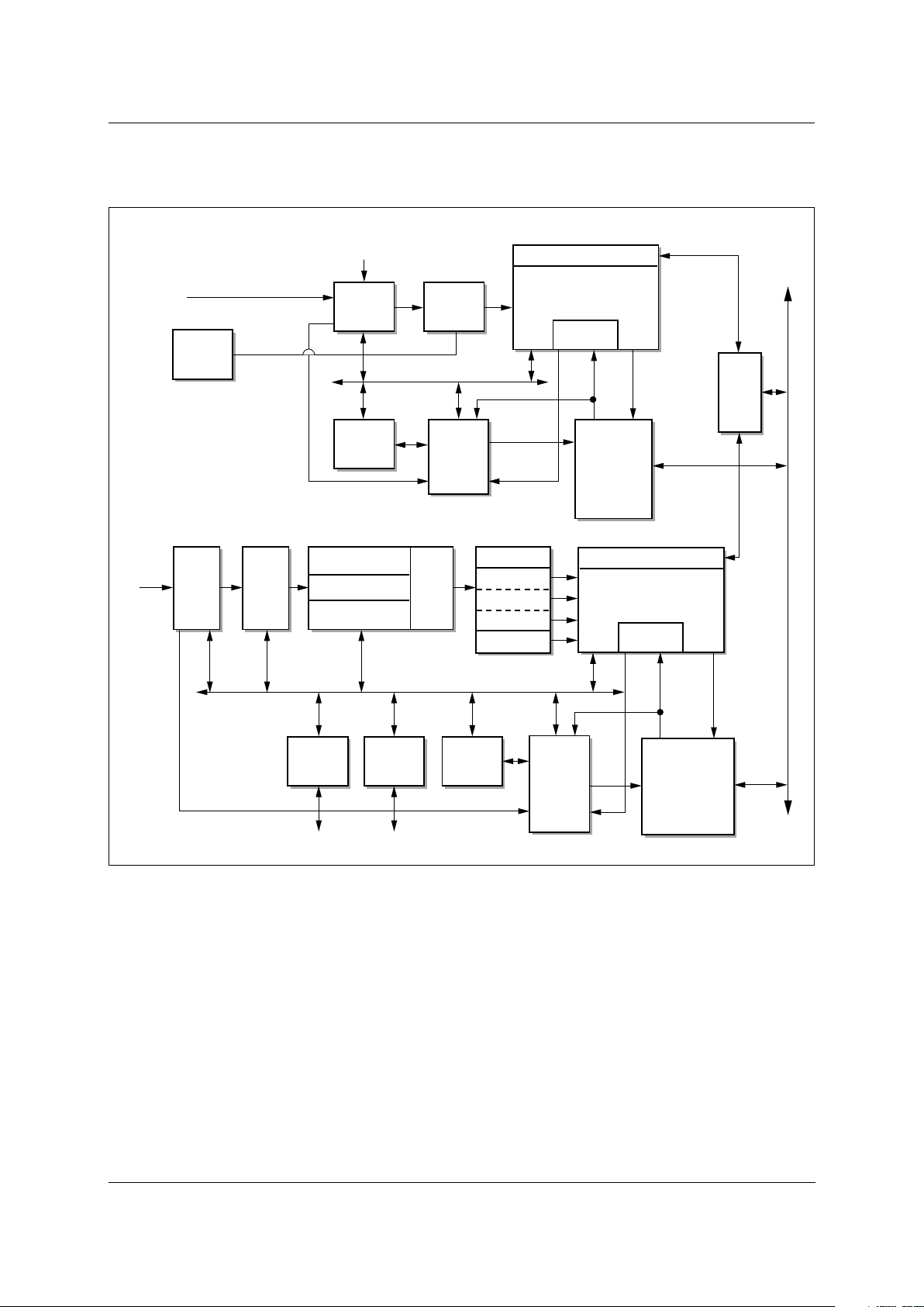
Figure 1-2. Fusion 878A Audio/Video Decoder and Scaler Block Diagram
Composite 1
Composite 2
Composite 3
Composite/S-Video (Y)
S-Video (C)
CIN
AGCCAP
REFP
XTO
XTI
STV TV-Audio
SFM Radio-Audio
SML Mic or Line-Level
Audio
ADATA
ALRCK
ASCLK
Digital
Audio (I
2
S)
Y
A/D
C
A/D
AGC
Clocking
Audio
A/D
Audio
Processing
Digital
Audio
Packetizer
Oversampling
Low-Pass Filter
Y/C
Separation
Chroma
Demod
Hue, Saturation,
and Brightness
Adjust
Horizontal and
Vertical Filtering
and Scaling
Video Data
Format Converter
Audio FIFO
879A_003
Page 16

1.0 Product Overview Fusion 878A
1.2 Detailed Features PCI Video Decoder
1-4 Conexant 100600B
1.2 Detailed Features
1.2.1 Video Capture
The Fusion 878A integrates an NTSC/PAL/SECAM composite and S-Video
decoder, scaler, DMA controller, and PCI Bus master on a single device. The
Fusion 878A can place video data directly into host memory for video capture
applications and into a target video display frame buffer for video overlay
applications. As a PCI initiator, the Fusion 878A can take control of the PCI bus
as soon as it is available, thereby avoiding the need for on-board frame buffers.
The Fusion 878A contains a pixel data FIFO to decouple the high speed PCI bus
from the continuous video data stream.
The video data input may be scaled, color translated, and burst-transferred to a
target location on a field basis. This allows for simultaneous preview of one field
and capture of the other field. Alternatively, the Fusion 878A is able to capture
both fields simultaneously or preview both fields simultaneously. The fields may
be interlaced into memory or sent to separate field buffers.
1.2.2 Audio Capture
The Fusion 878A can also capture the broadcast audio spectrum over the PCI bus.
This enables system solutions without the use of an analog audio cable. In
addition, the audio capture can be used to implement microphone audio capture
for complete videoconferencing applications.
1.2.3 Analog Video and Digital Camera Capture
The Fusion 878A includes a digital camera port to support digital video capture.
This specification defines the registers and functionality required for
implementing analog video capture support. Most of the analog and digital video
register settings are identical.
In addition to the standard CCIR 656 digital interface, the Fusion 878A can
accept digital video from digital cameras such as the Conexant Quartsight™,
Silicon Vision™, and Logitech™. Internally the digital stream is routed to the
high-quality down-scaler and color adjustment processing. It is then bus-mastered
into system memory or displayed via the graphics frame buffer.
1.2.4 Intel Intercast™ Support
The Fusion 878A fully supports the Intel Intercast technology. Intel Intercast
technology combines the programming of television and the Internet on the PC.
Page 17

Fusion 878A 1.0 Product Overview
PCI Video Decoder
1.2 Detailed Features
100600B Conexant 1-5
1.2.5 Video DMA Channels
The Fusion 878A enables separate destinations for the odd and even fields, each
controlled by a pixel RISC instruction list. This instruction list is created by the
Fusion 878A device driver and placed in the host memory. The instructions
control the transfer of pixels to target memory locations on a byte resolution
basis. Complex clipping can be accomplished by the instruction list, blocking the
generation of PCI bus cycles for pixels that are not to be seen on the display.
The DMA channels can be programmed on a field basis to deliver the video
data in packed or planar format. In packed mode, YCrCb data is stored in a single
continuous block of memory. In planar mode, the YCrCb data is separated into
three streams which are burst to different target memory blocks. Having the video
data in planar format is useful for applications where the data compression is
accomplished via software and the CPU.
1.2.6 Audio DMA Channels
The audio channel delivers 8-bit or 16-bit digital samples of a digital
frequency-multiplexed analog signal to system memory in packets of DWORDs.
A RISC program controls the audio DMA Program Initiator. The flow of audio
data and audio RISC instructions is completely independent and asynchronous to
the flow of video data and video RISC instructions.
Since the audio data path operates in continuous transfer mode (no sync gaps),
both the analog and the digital audio inputs can be used for other data capture
applications. The analog input offers 360 kHz usable BW at 8 effective bits or 100
kHz usable BW at 12 effective bits. The digital input offers up to 20 Mbps for the
parallel mode and 40 Mbps for the serial mode.
The audio DMA channel controller is similar to the video DMA controller in
that it supports packed mode RISC instructions. It also only interfaces to one
35 x 36 FIFO and its associated 6-bit DWORD counter.
The audio PCI initiator is identical to the video PCI initiator; they have the
same DMA controller interface and the same support for interrupts and
configuration space. Since the video and audio initiators are independent, each
can handle retries without inhibiting the other. Thus, the audio function can
initiate transfers to the host bridge even when a GFX target is retrying the video
function.
The audio PCI target is similar to the video PCI target with respect to
interrupts, configuration space, memory-mapped registers, and parity error
checking. The main difference in audio is that all of the memory-mapped
registers remain within the PCI clock and 32-bit interface domain. There is no
register interface to the audio clock domain. Thus, this target never issues a
disconnect or a retry.
1.2.7 Data Transport Engine
The Fusion 878A data transport engine operates in instruction mode. Video data
and audio data are delivered over the PCI bus under independent control.
Page 18

1.0 Product Overview Fusion 878A
1.2 Detailed Features PCI Video Decoder
1-6 Conexant 100600B
1.2.8 PCI Bus Interface
The Fusion 878A is designed to efficiently utilize the available 132 Mbps PCI
bus. The 32-bit DWORDs are output on the PCI bus with the appropriate image
data under the control of the DMA channels. The video stream consumes bus
bandwidth with average data rates varying from 44 Mbps for full size 768 x 576
PAL RGB32, to 4.6 Mbps for NTSC CIF 320 x 240 RGB16, to 0.14 Mbps for
NTSC ICON 80 x 60 8-bit mode.
The pixel instruction stream for the DMA channels consumes a minimum of
0.1 Mbps. The Fusion 878A provides the means for handling the bandwidth
bottlenecks caused by slow targets and long bus access latencies that can occur in
some system configurations. To overcome these system bottlenecks, the Fusion
878A gracefully degrades and recovers from FIFO overruns to the nearest pixel in
real time.
1.2.9 UltraLock™
The Fusion 878A employs a proprietary technique known as UltraLock to lock to
the incoming analog video signal. It always generates the required number of
pixels per line from an analog source in which line length can vary by as much as
a few microseconds. UltraLock’s digital locking circuitry enables the
VideoStream decoders to lock on to video signals quickly and accurately,
regardless of their source. Since the technique is completely digital, UltraLock
can recognize unstable signals caused by VCR head switches or any other
deviation and adapt the locking mechanism to accommodate the source.
UltraLock uses nonlinear techniques that are difficult, if not impossible, to
implement in genlock systems. And unlike linear techniques, it adapts the locking
mechanism automatically.
1.2.10 Scaling and Cropping
The Fusion 878A can reduce the video image size in both horizontal and vertical
directions independently, using arbitrarily selected scaling ratios. The X and Y
dimensions can be scaled down to one-sixteenth of the full resolution. Horizontal
scaling is implemented with a 6-tap interpolation f ilter, while up to 5-tap
interpolation is used for vertical scaling with a line store.
The video image can be arbitrarily cropped by reducing the number of active
scan lines and active horizontal pixels per line.
The Fusion 878A supports a temporal decimation feature that reduces video
bandwidth. This is accomplished by allowing frames or fields to be dropped from
a video sequence at fixed but arbitrarily selected intervals.
1.2.11 Input Interface
Analog video signals are input to the Fusion 878A via a four-input multiplexer.
The multiplexer can select between four composite source inputs or between three
composite and a single S-Video input source. When an S-Video source is input to
the Fusion 878A, the luma component is fed through the input analog multiplexer,
and the chroma component feeds directly into the C input pin. An AGC circuit
enables the Fusion 878A to compensate for non-standard amplitudes in the analog
signal input.
Page 19

Fusion 878A 1.0 Product Overview
PCI Video Decoder
1.2 Detailed Features
100600B Conexant 1-7
The clock signal interface consists of a pair of pins that connect to a 28.63636
MHz (8 × NTSC Fsc) crystal. Either fundamental or third harmonic crystals may
be used. Alternatively, CMOS oscillators may be used.
1.2.12 GPIO Port
The Fusion 878A provides a 24-bit GPIO bus. This interface can be used to input
or output up to 24 general purpose I/O signals. Alternatively, the GPIO port can
be used as a means to input video data. For example, the Fusion 878A can input
the video data from an external digital camera and bypass the Fusion 878A’s
internal video decoder block.
1.2.13 Vertical Blanking Interval Data Capture
The Fusion 878A provides a complete solution for capturing and decoding VBI
data. The Fusion 878A can operate in a VBI Line Output Mode, in which the VBI
data is only captured during select lines. This mode of operation enables
concurrent capture of VBI lines containing ancillary data and normal video image
data.
In addition, the Fusion 878A supports a VBI Frame Output Mode in which
every line in the video frame istreated as if it were a VBI line. This mode of
operation is designed for use with still frame capture/processing applications.
1.2.14 I2C Interface
The Fusion 878As I2C interface supports both 99.2 kHz timing transactions and
396.8 kHz, repeated start, multi-byte sequential transactions. As an I
2
C master,
Fusion 878A can program other devices on the video card, such as a TV tuner as
long as the device address is known. The Fusion 878A supports multi-byte
sequential reads (more than one transaction) and multi-byte write transactions
(greater than three transactions), which enable communication to devices that
support auto-incremental internal addressing.
1.2.15 HDTV Support
Fusion 878A has the ability to accept either serial or parellel HDTV data and
deliver that data to the host. Serial and parellel inputs both use the audio DMA
channel to transfer the HDTV MPEG packets to the host.
Serial HDTV streams may be input to the high speed serial port, which shares
pins with the digital audio (I
2
S) port. Fusion 878A will accept serial HDTV
streams at up to 40 Mbps.
Parellel HDTV data may be input to the GPIO port in asychronous parallel
mode at up to 20 Mbps.
Page 20
1.0 Product Overview Fusion 878A
1.3 Pin Descriptions PCI Video Decoder
1-8 Conexant 100600B
1.3 Pin Descriptions
Figure 1-3 displays the pinout diagram. Tabl e 1- 2 provides a description of pin
functions grouped by common function.
Figure 1-3. Fusion 878A Pinout Diagram
64
63
62
61
60
59
58
57
56
55
54
53
52
51
50
49
48
47
46
45
44
43
42
41
40
39
38
37
36
35
34
33
1
2
3
4
5
6
7
8
9
10
11
12
13
14
15
16
17
18
19
20
21
22
23
24
25
26
27
28
29
30
31
32
97
98
99
100
101
102
103
104
105
106
107
108
109
110
111
112
113
114
115
116
118
119
120
121
122
123
124
125
126
127
128
96
95
94
93
92
91
90
89
88
87
86
85
84
83
82
81
80
79
78
77
76
75
74
73
72
71
70
69
68
67
66
65
VDD
GNT
REQ
AD[31]
AD[30]
AD[29]
AD[28]
AD[27]
AD[26]
AD[25]
AD[24]
C
BE[3]
IDSEL
AD[23]
AD[22]
AD[21]
AD[20]
AD[19]
VDD
GND
AD[18]
AD[17]
AD[16]
C
BE[2]
FRAME
IRDY
TRDY
DEVSEL
STOP
PERR
SERR
PA R
GND
RST
INTA
TDI
TDO
TMS
TCK
TRST
MUX3
AGND
MUX2
MUX1
VAA
MUX0
AGND
REFP
AGCCAP
VAA
CIN
AGND
VCCAP
RBIAS
VCOMO
VCOMI
VRXP
VRXN
VBB
STV
BGND
SFM
BGND
C
BE[1]
AD[15]
AD[14]
AD[13]
AD[12]
VDD
GND
CLK
AD[11]
AD[10]
AD[09]
AD[08]
C
BE[0]
AD[07]
AD[06]
AD[05]
AD[04]
AD[03]
AD[02]
AD[01]
AD[00]
VDD
GND
GPIO[23]
GPIO[22]
GPIO[21]
GPIO[20]
GPIO[19]
GPIO[18]
XTI
XTO
GND
SMXC
VBB
SML
GND
VDD
SDA
SCL
ASCLK
GPIO[01]
GPIO[02]
GPIO[03]
GPIO[04]
GPIO[05]
GPIO[06]
GPIO[07]
GPIO[08]
GPIO[09]
GPIO[10]
GPIO[11]
GND
VDD
GPIO[12]
GPIO[13]
GPIO[14]
GPIO[15]
GPIO[16]
GPIO[17]
GPCLK
VDD
ALRCK
A DATA
GPIO[00]
Fusion 878A
117
VAA
879A_004
Page 21
Fusion 878A 1.0 Product Overview
PCI Video Decoder
1.3 Pin Descriptions
100600B Conexant 1-9
Table 1-2. Pin Descriptions Grouped by Pin Function (1 of 4)
Pin # Pin Name I/O Signal Description
PCI Interface (50 Pins)
(1)
40 CLK I Clock This input provides timing for all PCI transactions. All PCI
signals except RST
and INTA are sampled on the rising edge of
CLK, and all other timing parameters are defined with respect to
this edge. The Fusion 878A supports a PCI clock of up to
33.3333 MHz.
127 RST
I Reset This input three-states all PCI signals asynchronous to the CLK
signal.
3REQ
O Request Agent desires bus.
2GNTI Grant Agent granted bus.
13 IDSEL I Initialization
Device Select
This input is used to select the Fusion 878A during
configuration read and write transactions.
4–11,
14–18,
21–23,
34–37,
41–44,
46–53
AD[31:0] I/O Address/Data These three-state, bidirectional I/O pins transfer both address
and data information. A bus transaction consists of an address
phase followed by one or more data phases for either read or
write operations.
The address phase is the clock cycle in which FRAME
is first
asserted. During the address phase, AD[31:0] contains a byte
address for I/O operations and a DWORD address for
configuration and memory operations. During data phases,
AD[7:0] contains the least significant byte and AD[31:24]
contains the most significant byte.
Read data is stable and valid when TRDY
is asserted and
write data is stable and valid when IRDY
is asserted. Data is
transferred during the clocks when both TRDY
and IRDY are
asserted.
12, 24,
33, 45
CBE
[3:0] I/O Bus
Command/Byte
Enable
These three-state, bidirectional I/O pins transfer both bus
command and byte enable information. During the address
phase of a transaction, CBE
[3:0] signals contain the bus
command. During the data phase, CBE
[3:0] are used as byte
enables. The byte enables are valid for the entire data phase and
determine which byte lanes carry meaningful data. CBE
[3]
refers to the most significant byte and CBE
[0] refers to the least
significant byte.
32 PAR I/O Parity This three-state, bidirectional I/O pin provides even parity
across AD[31:0] and CBE
[3:0]. This means that the number of
1s on PAR, AD[31:0], and CBE
[3:0] equals an even number.
PAR is stable and valid one clock after the address phase. For
data phases, PAR is stable and valid one clock after either TRDY
is asserted on a read, or IRDY
is asserted on a write. Once valid,
PAR remains valid until one clock after the completion of the
current data phase. PAR and AD[31:0] have the same timing,
but PAR is delayed by one clock. The target drives PAR for read
data phases; the master drives PAR for address and write data
phases.
Page 22
1.0 Product Overview Fusion 878A
1.3 Pin Descriptions PCI Video Decoder
1-10 Conexant 100600B
25 FRAME I/O Cycle Frame This sustained, three-state signal is driven by the current master
to indicate the beginning and duration of an access. FRAME
is
asserted to signal the beginning of a bus transaction. Data
transfer continues throughout assertion. At de-assertion, the
transaction is in the final data phase.
26 IRDY
I/O Initiator Ready This sustained, three-state signal indicates the bus master’s
readiness to complete the current data phase.
IRDY
is used in conjunction with TRDY. When both IRDY and
TRDY
are asserted, a data phase is completed on that clock.
During a read, IRDY
indicates when the initiator is ready to
accept data. During a write, IRDY
indicates when the initiator
has placed valid data on AD[31:0]. Wait cycles are inserted until
both IRDY
and TRDY are asserted together.
28 DEVSEL
I/O Device Select This sustained, three-state signal indicates device selection.
When actively driven, DEVSEL
indicates the driving device has
decoded its address as the target of the current access.
27 TRDY
I/O Target Ready This sustained, three-state signal indicates the target’s
readiness to complete the current data phase.
IRDY is used in conjunction with TRDY. When both IRDY and
TRDY
are asserted, a data phase is completed on that clock.
During a read, TRDY
indicates when the target is presenting
data. During a write, TRDY
indicates when the target is ready to
accept the data. Wait cycles are inserted until both IRDY
and
TRDY
are asserted together.
29 STOP I/O Stop This sustained, three-state signal indicates the target is
requesting the master to stop the current transaction.
30 PERR
I/O Parity Error Report data parity error.
31 SERR O System Error Report address parity error. Open drain.
126 INTA O Interrupt A This signal is an open drain interrupt output.
JTAG (5 Pins)
122 TCK I Test Clock Used to synchronize all JTAG test structures. When JTAG
operations are not being performed, this pin must be driven to a
logical low.
123 TMS I Test Mode Select JTAG input pin whose transitions drive the JTAG state machine
through its sequences. When JTAG operations are not being
performed, this pin must be left floating or tied high.
125 TDI I Test Data Input JTAG pin used for loading instructions to the TAP controller or
for loading test vector data for boundary-scan operation. When
JTAG operations are not being performed, this pin must be left
floating or tied high.
124 TDO O Test Data Output JTAG pin used for verifying test results of all JTAG sampling
operations. This output pin is active for certain JTAG operations
and will be three-stated at all other times.
121 TRST
I Test Reset JTAG pin used to initialize the JTAG controller. When JTAG
operations are not being performed, this pin must be driven to a
logical low.
Table 1-2. Pin Descriptions Grouped by Pin Function (2 of 4)
Pin # Pin Name I/O Signal Description
Page 23

Fusion 878A 1.0 Product Overview
PCI Video Decoder
1.3 Pin Descriptions
100600B Conexant 1-11
I2C Interface (2 Pins)
90 SCL I/O Serial Clock Bus clock, output open drain.
91 SDA I/O Serial Data Bit Data or Acknowledge, output open drain.
General Purpose I/O (25 Pins)
66 GPCLK I/O GP Clock Video clock. Internally pulled up to VDD.
56–61,
67–72,
75–86
GPIO[23:0] I/O General Purpose
I/O
Fusion 878A pin decoding in normal mode. Pins pulled up to
VDD. For additional information, see Tables 3-3 and 3-5.
Digital Audio Input/Audio Test Signals (3 Pins)
87 ADATA I/O Audio Data Bit serial data.
88 ALRCK I/O Audio Clock Left/right framing clock.
89 ASCLK I/O Audio Serial Clock Bit serial clock.
Reference Timing Interface Signals (2 Pins)
62 XTI I A 28.63636 MHz crystal can be tied directly to these pins, or a
single-ended oscillator can be connected to XTI.
63 XTO O
Video Input Signals (7 Pins)
114, 116,
118, 120
MUX[0:3] I Analog composite video inputs to the on-chip 4:1 analog
multiplexer. Unused inputs should be tied to AGND. The output
of the MUX is direct-coupled to Y-A/D.
112 REFP A The top of the reference ladder for the video A/Ds. Connect to a
0.1 µF decoupling capacitor to AGND.
111 AGCCAP A The AGC time-constant control capacitor node. Must be
connected to a 0.1µF capacitor to AGND.
109 CIN I Analog chroma input to the C-A/D.
TV/Radio Audio Input Signals (10 Pins)
100 STV I TV sound input from TV tuner.
98 SFM I FM sound input from FM tuner.
94 SML I MIC/line input.
96 SMXC A Audio MUX anti-alias filter RC node. Connect through 68 pF
capacitor to BGND.
106 RBIAS A
Connection point for external bias 9.53 k
Ω 1% resistor.
105 VCOMO A Common mode voltage for the audio analog circuitry. This pin
should be connected to an external filtering 0.1 µF capacitor.
104 VCOMI A Common mode voltage for the audio analog circuitry. This pin
should be connected to an external filtering 0.1 µF capacitor.
107 VCCAP A Audio analog voltage compensation capacitor. This pin should
be connected to an external filtering 0.1 µF capacitor.
Table 1-2. Pin Descriptions Grouped by Pin Function (3 of 4)
Pin # Pin Name I/O Signal Description
Page 24

1.0 Product Overview Fusion 878A
1.3 Pin Descriptions PCI Video Decoder
1-12 Conexant 100600B
103 VRXP A Audio input circuitry reference voltage. This pin should be
connected to an external filtering 0.1 µF capacitor.
102 VRXN A Audio input circuitry reference voltage. This pin should be
connected to an external filtering 0.1 µF capacitor.
I/O and Core Power and Ground (14 Pins)
1, 19, 38,
54, 65 73,
92
VDD P Digital outputs power supply.
20, 39,
55, 64,
74, 93,
128
GND G Digital outputs ground.
Analog Video Power and Ground (6 Pins)
108 AGND A C video A/D ground and CREFN. Connect to analog ground
AGND.
110 VAA A Charge pump power supply and C video A/D power. Connect to
analog power VAA and a 0.1µF decoupling capacitor to AGND.
113 AGND A Charge pump ground return.
115 VAA A Y video A/D power. Connect to analog power VAA and a 0.1µF
decoupling capacitor to AGND.
117 VAA A Y video A/D power. Connect to analog power VAA and a 0.1µF
decoupling capacitor to AGND.
119 AGND A Y video A/D ground. Connect to analog ground AGND.
Analog Audio Power and Ground (4 Pins)
95, 101 VBB P Audio A/D power supply.
97, 99 BGND G Ground for audio A/D.
NOTE(S):
(1)
See PCI Specification 2.2 for further documentation.
2. I/O Column Legend:
I = Digital Input
O = Digital Output
I/O= Digital Bidirectional
A= Analog
G = Ground
P= Power
Table 1-2. Pin Descriptions Grouped by Pin Function (4 of 4)
Pin # Pin Name I/O Signal Description
Page 25

100600B Conexant 2-1
2
2.0 Functional Description
2.1 UltraLockTM Functionality
2.1.1 The Challenge
The line length (the interval between the midpoints of the falling edges of
succeeding horizontal sync pulses) of analog video sources is not constant. For a
stable source such as studio quality source or test signal generators, this variation
is very small:
±2 ns. However, for an unstable source such as a VCR, laser disk
player, or TV tuner, line length variation is as much as a few microseconds.
Digital display systems require a fixed number of pixels per line despite these
variations. The Fusion 878A employs a technique known as UltraLock to
implement locking the horizontal sync and the subcarrier of the incoming analog
video signal, generating the required number of pixels per line.
2.1.2 Operating Principles of UltraLock
UltraLock is based on sampling using a fixed-frequency, stable clock. Since the
video line length will vary, the number of samples generated using a
fixed-frequency sample clock will also vary from line to line. If the number of
generated samples per line is always greater than the number of samples per line
required by the particular video format, the number of acquired samples can be
reduced to fit the required number of pixels per line.
The Fusion 878A requires an 8 × Fsc (28.63636 MHz for NTSC and 35.46895
MHz for PAL) reference time source. The 8 × Fsc clock signal, or CLK x 2, is
divided down to CLK x 1 internally (14.31818 MHz for NTSC and 17.73 MHz
for PAL). CLK x 2 and CLK x 1 are internal signals and are not made available to
the system. UltraLock operates at CLK x 1 although the input waveform is
sampled at CLK x 2 then low-pass filtered and decimated to CLK x 1 sample rate.
At a 4 × Fsc (CLK x 1) sample rate there are 910 pixels for NTSC and 1,135
pixels for PAL/SECAM within a nominal line time interval (63.5
µs for NTSC
and 64
µs for PAL/SECAM). For square pixel NTSC and PAL/SECAM formats,
there should only be 780 and 944 pixels per video line, respectively. This is
because the square pixel clock rates are slower than a 4 × Fsc clock rate; for
example, 12.27 MHz for NTSC and 14.75 MHz for PAL.
UltraLock accommodates line length variations from nominal in the incoming
video by always acquiring more samples, at an effective 4 × Fsc rate, than are
required by the particular video format and outputting the correct number of
Page 26
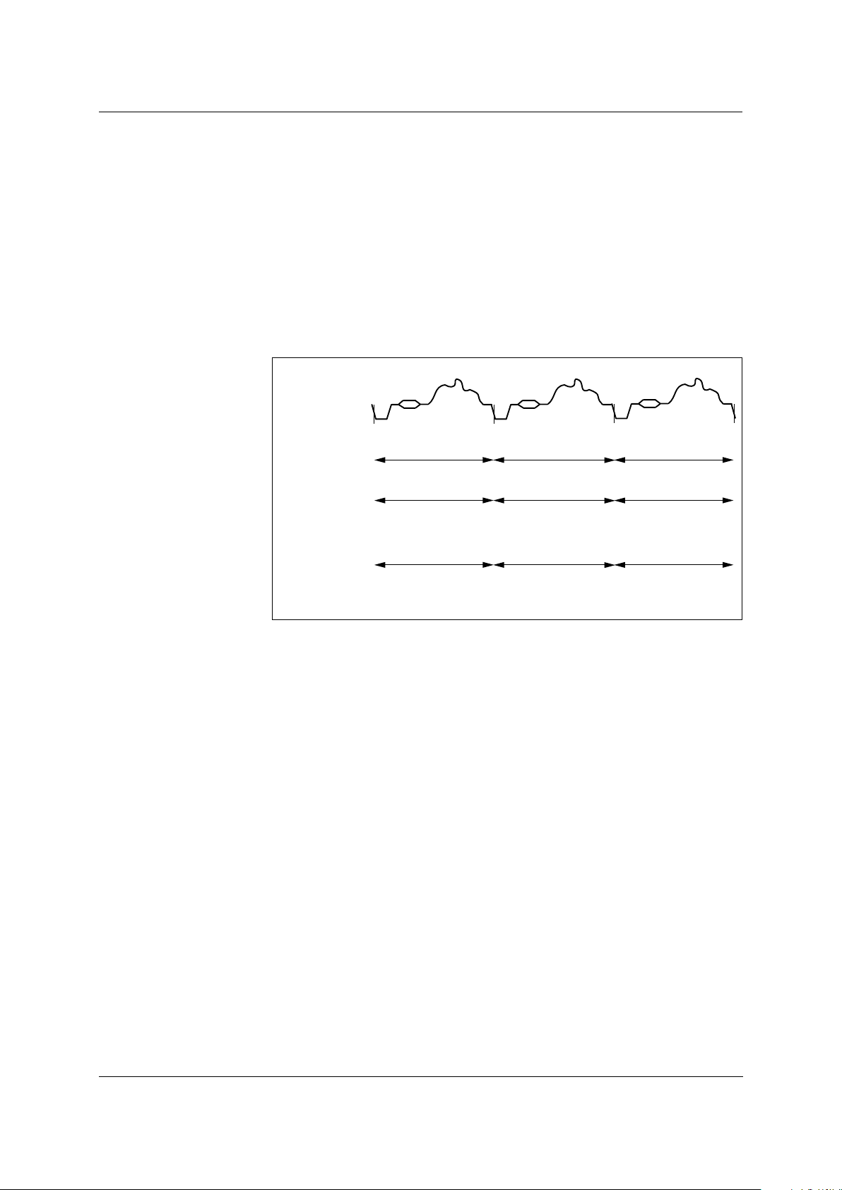
2.0 Functional Description Fusion 878A
2.1 UltraLockTM Functionality PCI Video Decoder
2-2 Conexant 100600B
pixels per line. UltraLock then interpolates the required number of pixels in a way
that maintains the stability of the original image despite variation in the line
length of the incoming analog waveform.
Figure 2-1 illustrates an example of three successive lines of video being
decoded for square pixel NTSC output. The first line is shorter than the nominal
NTSC line time interval of 63.5
µs. On this line, a line time of 63.2 µs sampled at
4 × Fsc (14.31831 MHz) generates only 905 pixels. The second line matches the
nominal line time of 63.5
µs and provides the expected 910 pixels. Finally, the
third line is too long at 63.8 µs within which 913 pixels are generated. In all three
cases, UltraLock outputs only 780 pixels.
UltraLock can be used to extract any programmable number of pixels from the
original video stream as long as the sum of the nominal pixel line length (910 for
NTSC and 1,135 for PAL/SECAM) and the worst case line length validation from
nominal in the active region is greater than or equal to the required number of
output pixels per line; i.e.,
NOTE: With stable inputs, UltraLock guarantees the time between the falling
edges of HRESET to within only one pixel. UltraLock does, however,
guarantee the number of active pixels in a line as long as the above
relationship holds.
Figure 2-1. UltraLock Behavior for NTSC Square Pixel Output
Analog
Waveform
63.2 µs 63.5 µs 63.8 µs
905 pixels 910 pixels 913 pixels
Line
Length
Pixels
Per Line
780 pixels 780 pixels 780 pixels
Pixels
Sent to
the FIFO
by
UltraLock™
879A_005
P
NomPVar
+ P
Desired
≥
where: P
Nom
= Nominal number of pixels per line at 4 × Fsc sample rate
(910 for NTSC, 1,135 for PAL/SECAM)
P
Var
= Variation of pixel count from nominal at 4 × Fsc (can be
a positive or negative number)
P
Desired
= Desired number of output pixels per line
Page 27
Fusion 878A 2.0 Functional Description
PCI Video Decoder
2.2 Composite Video Input Formats
100600B Conexant 2-3
2.2 Composite Video Input Formats
Fusion 878A supports several composite video input formats. Tab le 2 -1 shows the
video formats and some of the countries in which each format is used.
The video decoder must be programmed appropriately for each of the
composite video input formats. Table 2-2 lists the register values that need to be
programmed for each input format.
Table 2-1. Video Input Formats Supported by the Fusion 878A
Format Lines Fields F
SC
Country
NTSC-M 525 60 3.58 MHz U.S., many others
NTSC-Japan
(1)
525 60 3.58 MHz Japan
PAL-B, G, H 625 50 4.43 MHz Western/Central Europe, others
PAL-D 625 50 4.43 MHz China
PAL-I 625 50 4.43 MHz U.K., Ireland, South Africa
PAL-M 525 60 3.58 MHz Brazil
PAL-N
C
625 50 3.58 MHz Argentina
PAL-N 625 50 3.58 MHz Paraguay, Uruguay
SECAM 625 50 4.406 MHz, 4.250 MHz Eastern Europe, France, Middle East
NOTE(S):
(1)
NTSC—Japan has 0 IRE setup.
Table 2-2. Register Values for Square Pixel Video Input Formats
Register Bit NTSC-M NTSC-Japan
PAL-B, D,
G, H, I
PAL-M PAL-N
PAL-N
Combination
SECAM
IFORM
(0x01)
FORMAT
[2:0]
001 010 011 100 101 111 110
Cropping:
HDELAY
VDELAY
VACTIVE
CROP
HACTIVE
[7:0] in
all five
registers
Set to
desired
cropping
values in
registers
Set to
NTSC-M
square pixel
values
Set to
desired
cropping
values in
registers
Set to
NTSC-M
square pixel
values
Set to PAL-B, D, G, H, I square pixel
values
HSCALE [15:0] 0x02AC 0x02AC 0x033C 0x02AC 0x033C
0x033C
(1)
0x033C
ADELAY [7:0] 0x70 0x70 0x7F 0x70 0x7F 0x7F 0x7F
BDELAY [7:0] 0x5D 0x5D 0x72 0x5D 0x72 0x72 0xA0
NOTE(S):
(1)
The Fusion 878A will not output square pixel resolution for PAL N-combination. A smaller number of pixels must be output.
Page 28
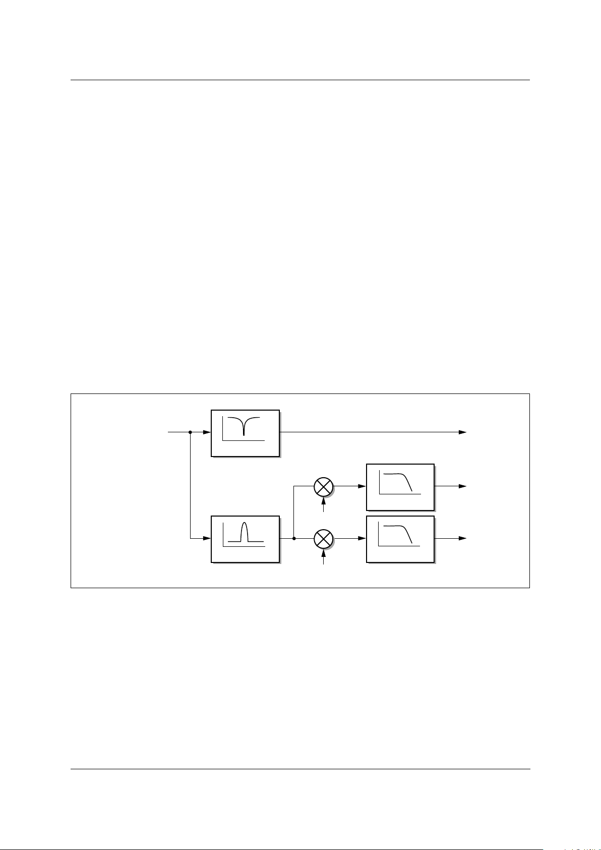
2.0 Functional Description Fusion 878A
2.3 Y/C Separation and Chroma Demodulation PCI Video Decoder
2-4 Conexant 100600B
2.3 Y/C Separation and Chroma Demodulation
Figure 2-2 illustrates Y/C separation and chroma decoding. Band-pass and notch
filters are implemented to separate the composite video stream. The filter
responses are illustrated in Figure 2-3. The optional chroma comb filter is
implemented in the vertical scaling block. See Section 2.4.
Figure 2-4 schematically describes the filtering and scaling operations.
In addition to the Y/C separation and chroma demodulation illustrated in
Figure 2-2, the Fusion 878A also supports chrominance comb filtering as an
optional filtering stage after chroma demodulation. The chroma demodulation
generates baseband I and Q (NTSC) or U and V (PAL/SECAM) color difference
signals.
For S-Video operation, the digitized luma data bypasses the Y/C separation
block completely and the digitized chrominance is passed directly to the chroma
demodulator.
For monochrome operation, the Y/C separation block must be disabled and the
saturation registers (SAT_U and SAT_V) are set to 0.
Figure 2-2. Y/C Separation and Chroma Demodulation for Composite Video
Notch Filter
Band Pass Filter
Low Pass Filter
Low Pass Filter
sin
cos
Y
U
V
Composite
879A_006
Page 29
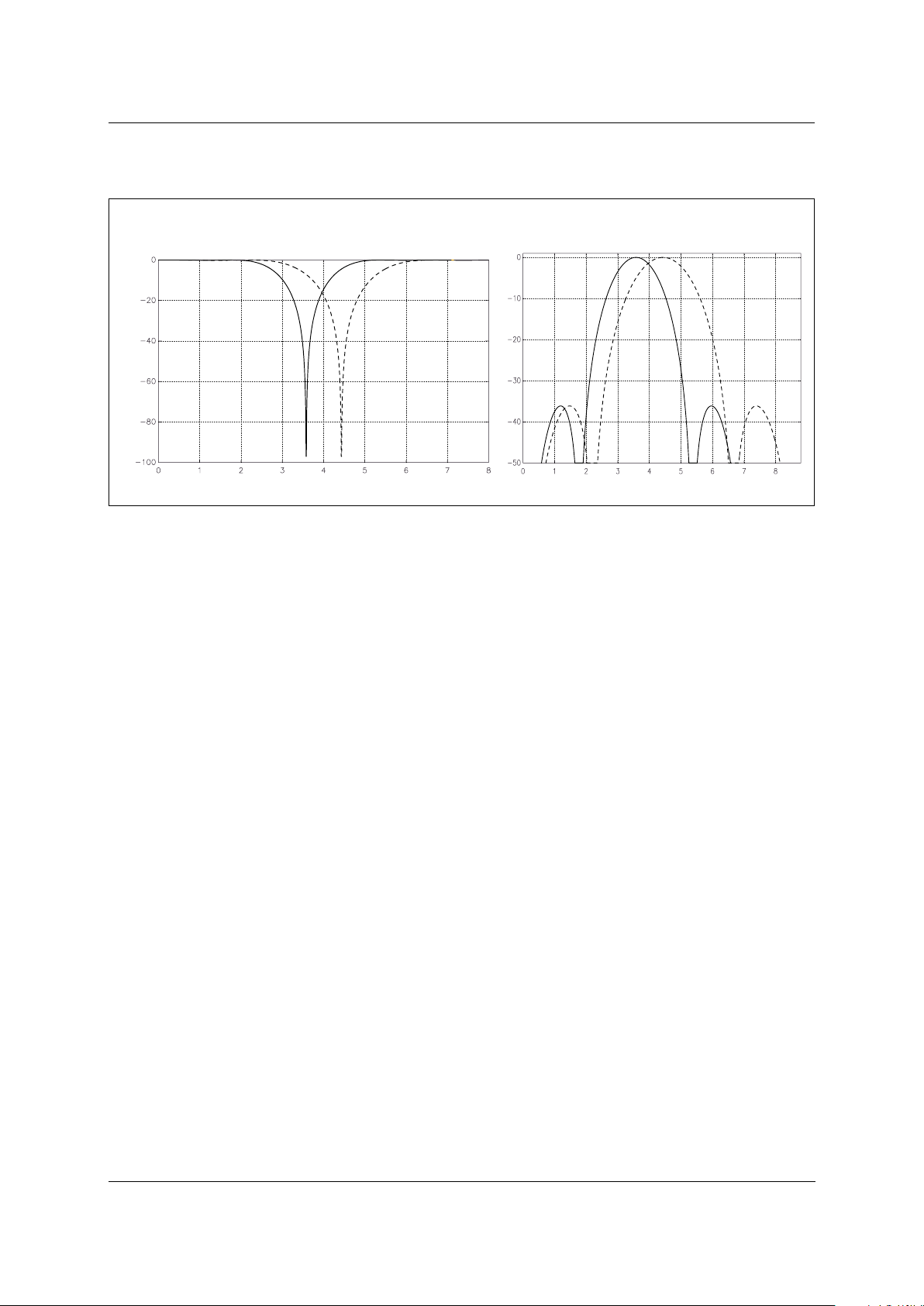
Fusion 878A 2.0 Functional Description
PCI Video Decoder
2.3 Y/C Separation and Chroma Demodulation
100600B Conexant 2-5
Figure 2-3. Y/C Separation Filter Responses
NTSC
PAL/SECAM
NTSC
PAL/SECAM
Luma Notch Filter Frequency Responses
for NTSC and PAL/SECAM
Chroma Band Pass Filter Frequency Responses
for NTSC and PAL/SECAM
879A_007
Amplitude in dB [20*log10(ampl)]
Frequency in MHzFrequency in MHz
Page 30
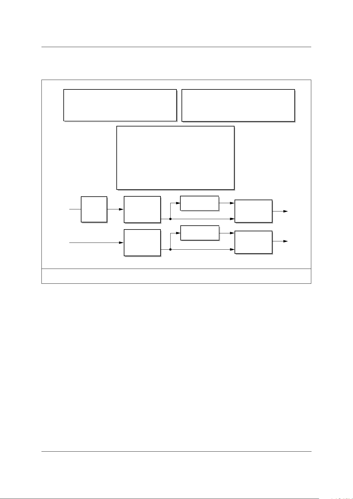
2.0 Functional Description Fusion 878A
2.3 Y/C Separation and Chroma Demodulation PCI Video Decoder
2-6 Conexant 100600B
Figure 2-4. Filtering and Scaling
NOTE(S): Z
–1
refers to a pixel delay in the horizontal direction, and a line delay in the vertical direction. The coefficients are
determined by UltraLock and the scaling algorithm.
Chrominance
1
2
---
1
2
---Z1–+=
Luminance CDZ
1–
+=
Vertical Scaler
Luminance
ABZ1–CZ2–DZ3–EZ4–FZ
5–
+++++=
Chrominance GHZ
1–
+=
Horizontal Scaler
6-Tap, 32-Phase
Interpolation
On-chip Memory
and
Horizontal
Scaling
On-chip Memory
and
Chroma Comb
Low Pass
Filter
Y
Y
C
C
Optional
Horizontal
Vertical Scaling
Luma Comb
(Chroma Comb)
3 MHz
1
4
---1 2
Z
1–
1Z
2–
++()=
1
8
---1 3
Z
1–
3Z2–1Z
3–
+++()=
1
16
------ 1 4
Z
1–
6Z2–4Z
3–
Z
4–
++++()=
Vertical Filter Options
Vertical Scaling
Vertical Filtering
Luminance
1
2
---1 z1–+()=
2-Tap, 32-Phase
Interpolation
and
Horizontal
Scaling
879A_008
Page 31

Fusion 878A 2.0 Functional Description
PCI Video Decoder
2.4 Video Scaling, Cropping, and Temporal Decimation
100600B Conexant 2-7
2.4 Video Scaling, Cropping, and Temporal
Decimation
The Fusion 878A provides three mechanisms to reduce the amount of video pixel
data in its output stream: down-scaling, cropping, and temporal decimation. All
three can be controlled independently.
2.4.1 Down-Scaling
2.4.1.1 Horizontal and
Vertical Scaling
The Fusion 878A provides independent and arbitrary horizontal and vertical
down- scaling. The maximum scaling ratio is 16:1 in both X and Y dimensions.
The maximum vertical scaling ratio is reduced from 16:1 (when using frames) to
8:1 (when using fields). The different methods used for scaling luminance and
chrominance are described in the following sections.
2.4.1.2 Field Aligned
Vertical Scaling
If Common Interchange Format (CIF) resolution video is viewed at 60/50 Hz
rates, then the video f ields must be field-aligned for proper overlay (sequenced on
top of each other successively). This could be done in interlaced Vertical Scaling
mode (INT set) which group delays (filters) only one field by one line. The two
fields are vertically aligned for overlay, but the two fields have different
frequency responses. One has not been filtered, while the other has been
line-averaged. A new option exists to filter both fields in a similar manner yet
maintain proper field alignment. This mode is selected by setting VSFLDALIGN
and resetting the INT bit to non-interlaced Vertical Scaling mode.
2.4.1.3 Luminance
Scaling
Horizontal Scaling The first stage in horizontal luminance scaling is an optional pre-filter which
provides the capability to reduce anti-aliasing artifacts. It is generally desirable to
limit the bandwidth of the luminance spectrum prior to performing horizontal
scaling because the scaling of high-frequency components may create image
artifacts in the resized image. The optional low pass filters illustrated in
Figure 2-5 reduce the horizontal high-frequency spectrum in the luminance
signal. Figure 2-6 and Figure 2-7 illustrates the combined results of the optional
low-pass filters, the luma notch filter and the 2x oversampling filter. Figure 2-8
illustrates the combined responses of the luma notch filter and the 2x
oversampling filter.
The Fusion 878A implements horizontal scaling through poly-phase
interpolation. The Fusion 878A uses 32 different phases to accurately interpolate
the value of a pixel. This provides an effective pixel jitter of less than 6 ns.
In simple pixel- and line-dropping algorithms, non-integer scaling ratios
introduce a step function in the video signal that effectively introduces
high-frequency spectral components. Poly-phase interpolation accurately
interpolates to the correct pixel and line position providing more accurate
information. This results in aesthetically pleasing video as well as higher
compression ratios in bandwidth limited applications.
Page 32

2.0 Functional Description Fusion 878A
2.4 Video Scaling, Cropping, and Temporal Decimation PCI Video Decoder
2-8 Conexant 100600B
Figure 2-5. Optional Horizontal Luma Low-Pass Filter Responses
NTSC PAL/SECAM
ICON
QCIF
CIF ICON
QCIF
CIF
Amplitude in dB [20*log10(ampl)]
Amplitude in dB [20*log10(ampl)]
Frequency in MHz Frequency in MHz
879A_009
Figure 2-6. Combined Luma Notch, 2x Oversampling and Optional Low-Pass Filter Response (NTSC)
ICON
QCIF
CIF
ICON
QCIF
CIF
Pass Band
Full Spectrum
Amplitude in dB [20*log10(ampl)]
Amplitude in dB [20*log10(ampl)]
Frequency in MHz Frequency in MHz
879A_010
Page 33

Fusion 878A 2.0 Functional Description
PCI Video Decoder
2.4 Video Scaling, Cropping, and Temporal Decimation
100600B Conexant 2-9
Vertical Scaling For vertical scaling, the Fusion 878A uses a line store to implement four different
filtering options. The f ilter characteristics are illustrated in Figure 2-9. The
Fusion 878A provides up to 5-tap filtering to ensure removal of aliasing artifacts.
The Video Timing Control (VTC) register sets the number of taps in the
vertical filter. The user may select 2, 3, 4 or 5 taps. The number of taps must be
chosen in conjunction with the horizontal scale factor in order to ensure the
needed data fits in the internal FIFO (see the VFILT bits in the VTC register for
limitations). As the scaling ratio is increased, the number of taps available for
vertical scaling increases. In addition to low-pass filtering, vertical interpolation
is also employed to minimize artifacts when scaling to non-integer scaling ratios.
Figure 2-7. Combined Luma Notch, 2x Oversampling and Optional Low-Pass Filter Response (PAL/SECAM)
ICON
QCIF
CIF
ICON
QCIF
CIF
Pass Band
Full Spectrum
Amplitude in dB [20*log10(ampl)]
Amplitude in dB [20*log10(ampl)]
Frequency in MHz
Frequency in MHz
879A_011
Figure 2-8. Combined Luma Notch and 2x Oversampling Filter Response
NTSC
PAL/SECAM
Amplitude in dB [20*log10(ampl)]
Frequency in MHz
879A_012
Page 34

2.0 Functional Description Fusion 878A
2.4 Video Scaling, Cropping, and Temporal Decimation PCI Video Decoder
2-10 Conexant 100600B
2.4.1.4 Peaking The Fusion 878A enables four different peaking levels by programming the
PEAK bit and HFILT bits in the SCLOOP register. The f ilters are illustrated in
Figure 2-10 and Figure 2-11. For more information, refer to SC Loop Control
Register.
Figure 2-9. Frequency Responses for the Four Optional Vertical Luma Low-Pass Filters
2-tap
3-tap
4-tap
5-tap
Amplitude in dB [20*log10(ampl)]
879A_013
Frequency/Sampling_Frequency
Page 35

Fusion 878A 2.0 Functional Description
PCI Video Decoder
2.4 Video Scaling, Cropping, and Temporal Decimation
100600B Conexant 2-11
Figure 2-10. Peaking Filters
HFILT = 01
HFILT = 10
HFILT = 11
HFILT = 00
Amplitude in dB [20*log10(ampl)]
879A_014
Frequency in MHz
HFILT = 01
HFILT = 11
HFILT = 10
HFILT = 00
Enhanced Resolution of Passband
Amplitude in dB [20*log10(ampl)]
879A_015
Frequency in MHz
Page 36

2.0 Functional Description Fusion 878A
2.4 Video Scaling, Cropping, and Temporal Decimation PCI Video Decoder
2-12 Conexant 100600B
Figure 2-11. Luma Peaking Filters with 2x Oversampling Filter and Luma Notch (1 of 2)
HFILT = 10
HFILT = 01
HFILT = 11
HFILT = 00
HFILT = 01
HFILT = 11
HFILT = 10
HFILT = 00
Enhanced Resolution of Passband
879A_016
Amplitude in dB [20*log10(ampl)]
Amplitude in dB [20*log10(ampl)]
Frequency in MHz
Frequency in MHz
Page 37

Fusion 878A 2.0 Functional Description
PCI Video Decoder
2.4 Video Scaling, Cropping, and Temporal Decimation
100600B Conexant 2-13
2.4.1.5 Chrominance
Scaling
A 2-tap, 32-phase interpolation filter is used for horizontal scaling of
chrominance. Vertical scaling of chrominance is implemented through
chrominance comb filtering using a line store, followed by simple decimation or
line dropping.
2.4.1.6 Scaling
Registers
The Horizontal Scaling
Ratio Register (HSCALE)
HSCALE is programmed with the horizontal scaling ratio. When outputting
unscaled video (in NTSC), the Fusion 878A produces 910 pixels per line. This
corresponds to the pixel rate at fCLK x 1 (4 × Fsc). This register is the control for
scaling the video to the desired size. For example, square pixel NTSC requires
780 samples per line, while CCIR 601 requires 858 samples per line.
HSCALE_HI and HSCALE_LO are two 8-bit registers that, when concatenated,
form the 16-bit HSCALE register. The method below uses pixel ratios to
determine the scaling ratio. The following formula should be used to determine
the scaling ratio to be entered into the 16-bit register:
Figure 2-11. Luma Peaking Filters with 2x Oversampling Filter and Luma Notch (2 of 2)
HFILT = 01
HFILT = 11
HFILT = 10
HFILT = 00
Enhanced Resolution of Passband
879A_016a
Amplitude in dB [20*log10(ampl)]
Frequency in MHz
NTSC: HSCALE = [ ( 910/P
desired
) – 1] × 4096
PAL/SECAM: HSCALE = [ ( 1135/P
desired
) – 1] × 4096
where: P
desired
= Desired number of pixels per line of video, including
active, sync and blanking.
Page 38

2.0 Functional Description Fusion 878A
2.4 Video Scaling, Cropping, and Temporal Decimation PCI Video Decoder
2-14 Conexant 100600B
For example, to scale PAL/SECAM input to square pixel QCIF, the total
number of horizontal pixels desired is 236:
An alternative method for determining the HSCALE value uses the ratio of
the scaled active region to the unscaled active region as shown below:
In this equation, the HACTIVE value cannot be cropped; it represents the total
active region of the video line. This equation produces roughly the same result as
using the full line length ratio shown in the first example. However, due to
truncation, the HSCALE values determined using the active pixel ratio method
will be slightly different from those obtained using the total line length pixel ratio
method. The values in Tabl e 2-3, were calculated using the full line length ratio.
The Vertical Scaling
Ratio Register (VSCALE)
VSCALE is programmed with the vertical scaling ratio. It defines the number of
vertical lines output by the Fusion 878A. The following formula should be used
to determine the value to be entered into this 13-bit register. The loaded value is a
two’s-complement, negative value.
For example, to scale PAL/SECAM input to square pixel QCIF, the total
number of vertical lines is 156:
Only the 13 LSBs of the VSCALE value are used; the five LSBs of
VSCALE_HI and the 8-bit VSCALE_LO register form the 13-bit VSCALE
register. The three MSBs of VSCALE_HI are used to control other functions. The
user must take care not to alter the values of the three MSBs when writing a
vertical scaling value.
HSCALE = [ ( 1135/236 ) – 1 ] × 4096
= 12331
= 0 × 3CF2
NTSC: HSCALE = [ (754 / HACTIVE) – 1] × 4096
PAL/SECAM: HSCALE = [ (922 / HACTIVE) – 1] × 4096
where: HACTIVE = Desired number of pixels per line of video, not
including sync or blanking.
VSCALE = ( 0x10000 – { [ ( scaling_ratio ) – 1] × 512 } ) + 0x1FFF
VSCALE = ( 0x10000 – { [ ( 4/1 ) –1 ] × 512 } ) + 0x1FFF
= 0x1A00
Page 39

Fusion 878A 2.0 Functional Description
PCI Video Decoder
2.4 Video Scaling, Cropping, and Temporal Decimation
100600B Conexant 2-15
The following C-code fragment illustrates changing the vertical scaling value:
#define VSCALE_HI 0x13
#define VSCALE_LO 0x14
typedef unsigned char BYTE;
typedef unsigned int WORD;
BYTE ReadFromFusion878A(BYTE regAddress);
void WriteToFusion878A(BYTE regAddress, BYTE regValue);
void SetFusion878AVScaling(WORD VSCALE)
{
BYTE oldVscaleMSByte, newVscaleMSByte;
/* get existing VscaleMSByte value from */
/* Fusion878A VSCALE_HI register */
oldVscaleMSByte = ReadFromFusion878A(VSCALE_HI);
/* create a new VscaleMSByte, preserving top 3 bits */
newVscaleMSByte = (oldVscaleMSByte & 0xE0)|(VSCALE >>
8);
/* send the new VscaleMSByte to the VSCALE_HI reg */
WriteToFusion878A(VSCALE_HI, newVscaleMSByte);
/* send the new VscaleLSByte to the VSCALE_LO reg */
WriteToFusion878A(VSCALE_LO, (BYTE) VSCALE);
}
If your target machine has sufficient memory to statically store the scaling
values locally, the READ operation can be eliminated.
NOTE: When scaling below CIF resolution, it may be useful to use a single field
as opposed to using both fields. Using a single field will ensure there are
no inter-field motion artifacts on the scaled output. When performing
single field scaling, the vertical scaling ratio will be twice as large as when
scaling with both fields. For example, CIF scaling from one field does not
require any vertical scaling, but when scaling from both fields, the scaling
ratio is 50%. Also, the non-interlaced bit should be reset when scaling
from a single field (INT=0 in the VSCALE_HI register).
Table 2 -3 lists scaling ratios for various video formats and the register values
required.
where:
&
= bitwise AND
|
= bitwise OR
>>
= bit shift, MSB to LSB
Page 40

2.0 Functional Description Fusion 878A
2.4 Video Scaling, Cropping, and Temporal Decimation PCI Video Decoder
2-16 Conexant 100600B
2.4.2 Image Cropping
Cropping enables the user to output any subsection of the video image. The start
of the active area in the vertical direction is referenced to VRESET
(beginning of
a new field). In the horizontal direction it is referenced to HRESET
(beginning of
a new line). The dimensions of the active video region are defined by HDELAY,
HACTIVE, VDELAY, and VACTIVE. All four registers are 10-bit values. The
CROP register contains two MSBs of each register, while the lower eight bits are
in the respective HDELAY_LO, HACTIVE_LO, VDELAY_LO, and
VACTIVE_LO registers. The vertical and horizontal delay values determine the
position of the cropped image within a frame while the horizontal and vertical
active values set the pixel dimensions of the cropped image as illustrated in
Figure 2-12.
Table 2-3. Scaling Ratios for Popular Formats Using Frequency Values
Scaling Ratio Format Total Resolution
(1)
Output
Resolution
(Active Pixels)
HSCALE
Register
Values
VSCALE Register Values
Use Both
Fields
Single
Field
Full Resolution
1:1
NTSC SQ Pixel
NTSC CCIR601
PAL CCIR 601
PAL SQ Pixel
780x525
858x525
864x625
944x625
640x480
720x480
720x576
768x576
0x02AA
0x00F8
0x0504
0x033C
0x0000
0x0000
0x0000
0x0000
N/A
N/A
N/A
N/A
CIF
2:1
NTSC SQ Pixel
NTSC CCIR601
PAL CCIR 601
PAL SQ Pixel
390x262
429x262
432x312
472x312
320x240
360x240
360x288
384x288
0x1555
0x11F0
0x1A09
0x1679
0x1E00
0x1E00
0x1E00
0x1E00
0x0000
0x0000
0x0000
0x0000
QCIF
4:1
NTSC SQ Pixel
NTSC CCIR601
PAL CCIR 601
PAL SQ Pixel
195x131
214x131
216x156
236x156
160x120
180x120
180x144
192x144
0x3AAA
0x3409
0x4412
0x3CF2
0x1A00
0x1A00
0x1A00
0x1A00
0x1E00
0x1E00
0x1E00
0x1E00
ICON
8:1
NTSC SQ Pixel
NTSC CCIR601
PAL CCIR 601
PAL SQ Pixel
97x65
107x65
108x78
118x78
80x60
90x60
90x72
96x72
0x861A
0x7813
0x9825
0x89E5
0x1200
0x1200
0x1200
0x1200
0x1A00
0x1A00
0x1A00
0x1A00
NOTE(S):
(1)
Including sync and blanking interval.
Page 41

Fusion 878A 2.0 Functional Description
PCI Video Decoder
2.4 Video Scaling, Cropping, and Temporal Decimation
100600B Conexant 2-17
Figure 2-12. Effect of the Cropping and Active Registers
Beginning of a New Frame
Beginning of a New Line
Video frame
Horizontally ActiveHorizontally Inactive
Vertically
Vertically
Video frame
Horizontally
Horizontally Inactive
Vertically
Vertically
Cropped image
Cropped image
scaled to
1/2 size
Active
Inactive
Active
Inactive
Active
HRESET
VRESET
879A_017
Page 42

2.0 Functional Description Fusion 878A
2.4 Video Scaling, Cropping, and Temporal Decimation PCI Video Decoder
2-18 Conexant 100600B
2.4.2.1 Cropping
Registers
Horizontal Delay
Register (HDELAY)
For video decoding, HDELAY is programmed with the number of pixels between
horizontal sync and the first pixel of each line to be displayed or captured. For
GPIO SPIOUT, the HDELAY is programmed with the number of pixels between
the falling edge of HRESET and the rising edge of HACTIVE. HDELAY should
be an even number to get Cb as the first pixel, an odd number to get Cr.
The register value is programmed with respect to the scaled frequency clock.
Horizontal Active
Register (HACTIVE)
For video decoding, HACTIVE is programmed with the actual number of
displayed or captured pixels per line. For GPIO SPIOUT, HACTIVE is
programmed with the number of pixels that HACTIVE signal is high after the
HACTIVE signal goes high.
The register value is programmed with respect to the scaled frequency clock.
The video line can be considered a combination of three components:
1. Back porch and Sync: defined by HDELAY
2. Active Video: defined by HACTIVE
3. Front Porch: total scaled pixels—HDELAY through HACTIVE
For uncropped images, the square pixel values for these components at 4 × Fsc
are displayed in Ta bl e 2 -4 .
Therefore, for uncropped images the values are:
For cropped images, HDELAY can be increased and HACTIVE decreased so
that HDELAY + HACTIVE
≤ 889 × HSCALE for NTSC and ≤ 1108 × HSCALE
for PAL. If HDELAY + HACTIVE is too much, then you will see front or back
porch pixels. Regions of the video signal are illustrated in Table 2-13.
Table 2-4. Square Pixel Values
Video
Standard
CLK x 1
Front Porch
CLK x 1 HDELAY CLK x 1 HACTIVE
CLK x 1
Total
NTSC 21 135 754 910
PAL/SECAM 27 186 922 1135
HDELAY (NTSC) = (135/754 × HACTIVE) & 0x3FE
HDELAY(PAL) = (186/922 × HACTIVE) & 0x3FE
Figure 2-13. Regions of the Video Signal
HDELAY HACTIVE
Front
Porch
879A_018
Page 43

Fusion 878A 2.0 Functional Description
PCI Video Decoder
2.4 Video Scaling, Cropping, and Temporal Decimation
100600B Conexant 2-19
The Vertical Delay
Register (VDELAY)
For video decoding, VDELAY is programmed with the number of half lines
between the end of the serration pulses and the first line to be displayed or
captured.
For GPIO SPIOUT, VDELAY is programmed with the number of half lines
between the rising edge of VRESET
and the rising edge of VACTIVE.
The register value is programmed with respect to the unscaled input signal.
VDELAY must be programmed to an even number to avoid apparent field
reversal.
The Vertical Active
Register (VACTIVE)
For video decoding and GPIO SPIOUT, VACTIVE is programmed with the
number of lines in one frame for the source video.
NOTE: It is important to note the difference between the implementation of the
horizontal registers (HSCALE, HDELAY, and HACTIVE) and the vertical
registers (VSCALE, VDELAY, and VACTIVE). Horizontally, HDELAY
and HACTIVE are programmed with respect to the scaled pixels defined
by HSCALE. Vertically, VDELAY and VACTIVE are programmed with
respect to the number of lines before scaling (before VSCALE is applied).
For GPIO SPIIN, the registers HDELAY, HACTIVE, VDELAY, and
VACTIVE are not used.
2.4.3 Temporal Decimation
Temporal decimation provides a solution for video synchronization during
periods when full frame rate cannot be supported due to bandwidth and system
restrictions.
For example, when capturing live video for storage, system limitations such as
hard disk transfer rates or system bus bandwidth may limit the frame capture rate.
If these restrictions limit the frame rate to 15 frames per second, the Fusion 878As
time scaling operation enables the system to capture every other frame instead of
allowing hard disk timing restrictions to dictate which frame to capture. This
maintains an even distribution of captured frames and alleviates the “jerky” effect
caused by systems that simply burst in data when the bandwidth becomes
available.
The Fusion 878A provides temporal decimation on either a field or frame
basis. The temporal decimation register (TDEC) is loaded with a value from 1 to
60 (NTSC) or 1 to 50 (PAL/SECAM). This value is the number of fields or
frames skipped by the chip during a sequence of 60 for NTSC or 50 for
PAL/SECAM. Skipped fields and frames are considered inactive, which is
indicated by the ACTIVE pin remaining low.
Examples:
TDEC = 0x02 Decimation is performed by frames. Two frames are
skipped per 60 frames of video, assuming NTSC
decoding.
Frames 1–29 are output normally, then ACTIVE
remains low for one frame. Frames 31–59 are then
output followed by another frame of inactive video.
Page 44

2.0 Functional Description Fusion 878A
2.4 Video Scaling, Cropping, and Temporal Decimation PCI Video Decoder
2-20 Conexant 100600B
When changing the programming in the temporal decimation register, 0x00
should be loaded first, and then the decimation value. This ensures that the
decimation counter is reset to 0. If 0 is not loaded first, the decimation may start
on any field or frame in the sequence of 60 (or 50 for PAL/SECAM). On
power-up, this preload is not necessary because the counter is internally reset.
When decimating fields, the FLDALIGN bit in the TDEC register can be
programmed to choose whether the decimation starts with an odd field or an even
field. If the FLDALIGN bit is set to logical 0, the first field dropped during the
decimation process will be an odd field. Conversely, setting the FLDALIGN bit to
logical 1 causes the even field to be dropped f irst in the decimation process.
TDEC = 0x9E Decimation is performed by fields. Thirty fields are out-
put per 60 fields of video, assuming NTSC decoding.
This value outputs every other field (every odd field)
of video starting with field 1 in frame 1.
TDEC = 0x01 Decimation is performed by frames. One frame per 50
frames of video is skipped, assuming PAL/SECAM decoding.
TDEC = 0x00 Decimation is not performed. Full frame rate video is out-
put by the Fusion 878A.
Page 45

Fusion 878A 2.0 Functional Description
PCI Video Decoder
2.5 Video Adjustments
100600B Conexant 2-21
2.5 Video Adjustments
The Fusion 878A provides programmable hue, contrast, saturation, and
brightness.
2.5.1 The Hue Adjust Register
The Hue Adjust Register (HUE) is used to offset the hue of the decoded signal. In
NTSC, the hue of the video signal is defined as the phase of the subcarrier with
reference to the burst. The value programmed in this register is added to or
subtracted from the phase of the subcarrier, which effectively changes the hue of
the video. The hue can be shifted by ±90 degrees. Because of the nature of
PAL/SECAM encoding, hue adjustments can not be made when decoding
PA L / S E C A M.
2.5.2 The Contrast Adjust Register
The Contrast Adjust Register (CONTRAST) (also called the luma gain) provides
the ability to change the contrast from approximately 0% to 200% of the original
value. The decoded luma value is multiplied by the 9-bit coeff icient loaded into
this register.
2.5.3 The Saturation Adjust Registers
The Saturation Adjust Registers (SAT_U, SAT_V) are additional color
adjustment registers. It is a multiplicative gain of the U and V signals. The value
programmed in these registers are the coefficients for the multiplication. The
saturation range is from approximately 0% to 200% of the original value.
2.5.4 The Brightness Register
The Brightness Register (BRIGHT) is simply an offset for the decoded luma
value. The programmed value is added to or subtracted from the original luma
value which changes the brightness of the video output. The luma output is in the
range of 0 to 255. Brightness adjustment can be made over a range of –128 to
+127.
Page 46

2.0 Functional Description Fusion 878A
2.6 Automatic Chrominance Gain Control PCI Video Decoder
2-22 Conexant 100600B
2.6 Automatic Chrominance Gain Control
The Automatic Chrominance Gain Control (ACGC) compensates for reduced
chrominance and color-burst amplitudes. Here, the color-burst amplitude is
calculated and compared to nominal. The color-difference signals are then
increased or decreased in amplitude according to the color-burst amplitude
difference from nominal. The range of chrominance gain is 0.5–2 times the
original amplitude. This compensation coefficient is then multiplied by the
saturation adjust value for a total chrominance gain range of 0–2 times the
original signal. Automatic chrominance gain control may be disabled.
2.7 Low Color Detection and Removal
If a color-burst of 25 percent (NTSC) or 35 percent (PAL/SECAM) or less of the
nominal amplitude is detected for 127 consecutive scan lines, the color-difference
signals U and V are set to 0. When the low color detection is active, the reduced
chrominance signal is still separated from the composite signal to generate the
luminance portion of the signal. The resulting Cr and Cb values are 128. Output
of the chrominance signal is re-enabled when a color-burst of 43 percent (NTSC)
or 60 percent (PAL/SECAM) or greater of nominal amplitude is detected for 127
consecutive scan lines. Low color detection and removal may be disabled.
Page 47

Fusion 878A 2.0 Functional Description
PCI Video Decoder
2.8 Coring
100600B Conexant 2-23
2.8 Coring
The Fusion 878A video decoder can perform a coring function, in which it forces
all values below a programmed level to be 0. This is useful as the human eye is
more sensitive to variations in black images. By taking near-black images and
turning them into black, the image appears clearer to the eye.
Four coring values can be selected: 0, 8, 16, or 32 above black. If the total
luminance level is below the selected limit, the luminance signal is truncated to
the black value. If the luma range is limited (i.e., black is 16), then the coring
circuitry automatically takes this into account and references the appropriate
value for black. Coring is illustrated in Figure 2-14.
Figure 2-14. Coring Map
32
16
8
0
321680
Calculated
Luma Value
Output
Luma Value
879A_019
Page 48

2.0 Functional Description Fusion 878A
2.9 VBI Data Output Interface PCI Video Decoder
2-24 Conexant 100600B
2.9 VBI Data Output Interface
A frame of video is composed of 525 lines for NSTC and 625 for PAL/SECAM.
Figure 2-15 illustrates an NTSC video frame, in which there are a number of
distinct regions. The video image or picture data is contained in the odd and even
fields within lines 21 to 263 and lines 283 to 525, respectively. Each field of
video also contains a region for vertical synchronization (lines 1 through 9 and
264 through 272) as well as a region which can contain non-video ancillary data
(lines 10 through 20 and 273 through 283). These regions between the vertical
synchronization region and the video picture region are referred to as the VBI
portion of the video signal. Figure 2-16 illustrates the PAL video frame.
Figure 2-15. Regions of the NTSC Video Frame
Figure 2-16. Regions of the PAL Video Frame (Fields 1, 2, 5, and 6)
Lines 1–9
Lines 10–20
Lines 21–263
Lines 264–272
Lines 273–283
Lines 284–525
Vertical Blanking Interval
Video Image Region
Vertical Blanking Interval
Video Image Region
Odd FieldEven Field
Vertical Synchronization Region
Vertical Synchronization Region
879A_020
Lines 1–6
Lines 7–23
Lines 24–310
Lines 311–318
Lines 319–335
Lines 336–625
Vertical Blanking Interval
Video Image Region
Vertical Blanking Interval
Video Image Region
Odd FieldEven Field
Vertical Synchronization Region
Vertical Synchronization Region
879A_021
Page 49

Fusion 878A 2.0 Functional Description
PCI Video Decoder
2.9 VBI Data Output Interface
100600B Conexant 2-25
The Fusion 878A is able to capture VBI data and store it in the host memory
for later processing by the Fusion 878A VBI decoder software. Two modes of
VBI capture exist: VBI line output mode and VBI frame output mode. Both types
of data may be captured during the same field.
2.9.1 VBI Line Output Mode
In the VBI line output mode, VBI capture occurs during the vertical blanking
interval. The start of VBI data capture is set by the VBI_HDELAY bit in the VBI
Packet Size/Delay register, and is in reference to the trailing edge of the HRESET
signal. The number of DWORDs of VBI data is selected by the user. Each
DWORD contains 4 VBI bytes, and each VBI pixel consists of two VBI samples.
For example, for a given 800 pixel line in the VBI region, there exist 1600 VBI
samples, which are equivalent to 400 DWORDs of VBI data. The VBI_PKT_HI
and VBI_PKT_LO register bits are concatenated to create the 9-bit value for the
number of DWORDs to be captured.
VBI line data capture occurs when the CAPTURE_VBI_EVEN register bit is
enabled for the even field, and CAPTURE_VBI_ODD register bit is enabled for
the odd field. The VBI data is sampled at a rate of 8 × Fsc and is stored in the
FIFO as a sequence of 8-bit samples. Line mode VBI data starts horizontally
beginning at VBI_HDELAY pixels from the trailing edge of HRESET
and ending
after the VBI_PKT number of DWORDs. Line mode VBI data starts vertically
beginning at the f irst line following VRESET
and ending at VACTIVE. VBI
register settings can be changed only on a per-frame basis. The VBI timing is
illustrated in Figure 2-17.
Once the VBI data has been captured and stored in the Fusion 878A FIFO, it is
treated as any other type of data. It is output over the PCI bus via RISC
instructions. If the number of VBI lines desired by the user is smaller than the
entire vertical blanking region, the extra data will be discarded by the use of the
SKIP RISC instruction. Alternatively, if the user desires a larger VBI region in the
VBI line output mode, the vertical blanking region can be extended by setting the
VDELAY register to the appropriate value. The VBI line output mode can in
effect extend the VBI region to the entire field. Figure 2-18 illustrates a block
diagram of the VBI section.
Figure 2-17. VBI Timing
VBI Line Data Capture
VBI_PKT #
VBI_HDELAY
VACTIVE
VRESET
HRESET
VDELAY
879A_022
Page 50

2.0 Functional Description Fusion 878A
2.9 VBI Data Output Interface PCI Video Decoder
2-26 Conexant 100600B
In the VBI frame output mode, VBI data capture occurs in the active video
region and includes all the horizontal blank/sync information in the data stream.
This feature can be used to provide a high quality still-capture of video. The data
is vertically bound beginning at the first line during VACTIVE and ending after a
fixed number of packets. The data stream is packetized into a series of
256-DWORD blocks.
A fixed number of DWORD blocks (434 for NTSC and 650 for PAL) are
captured during each field. This is equivalent to 111,104 DWORDs for NTSC
(434 × 256 DWORDs) and 166,400 DWORDs for PAL (650 × 256 DWORDs) per
field. The VBI frame capture region can be extended to include the 10 lines prior
to the default VACTIVE region by setting the EXT_FRAME register bit.
VDELAY must also be set to its minimum value of 2. The extended DWORD
block size is 450 DWORD blocks for NTSC and 674 DWORD blocks for PAL.
The VBI frame data capture occurs during the even field when the
CAPTURE_EVEN register bit is set and the COLOR_EVEN bit is set to raw
mode, and during the odd field when the CAPTURE_ODD register bit is set and
the COLOR_ODD bit is set to raw mode. The captured data stream is continuous
and not aligned with HSYNC.
Figure 2-18. VBI Section Block Diagram
YCrCb 4:2:2, 4:1:1
CSC/Gamma
8-Bit Dither
Format
MUX
FIFOs
Y: 70x36
Cb: 35x36
Cr: 35x36
# Dwords
DMA Controller PCI Initiator
Instruction
Queue
Address Generator
FIFO Data MUX
PCI
Bus
Video Data Format Converter
VBI
Data
Analog
Video
ADC
879A_023
Page 51

Fusion 878A 2.0 Functional Description
PCI Video Decoder
2.10 Video Data Format Conversion
100600B Conexant 2-27
2.10 Video Data Format Conversion
2.10.1 Pixel Data Path
The video decoder/scaler portion of the Fusion 878A generates a video data
stream in packed 4:2:2 YCrCb format. The video data is then color
space-converted and formatted in a 32-bit wide DWORD. Figure 2-19 illustrates
the steps in converting the video data from packed 4:2:2 YCrCb to the desired
format. The YCrCb 4:2:2 data is up-sampled to 4:4:4 format prior to conversion
to RGB. It can then be dithered, have gamma correction removed, or be presented
directly to the byte swap circuit.
In the case where 4:1:1 data is desired, the 4:2:2 data is first down-sampled,
then packed into BtYUV format (see Table 2 -6 ) or converted to planar format and
vertically sub-sampled to achieve the YUV9 format. Alternatively, packed 4:2:2
data may be converted to planar 4:2:2 and vertically sub-sampled to YUV12
format. The vertical sub-sampling is achieved via the appropriate DMA
instructions (see Section 2.12).
Fusion 878A also offers a Y8 color format, in which the chroma component of
the packed 4:2:2 data is stripped and the luma component is packed into 8 bits.
This format is otherwise known as gray scale. Table 2-5 lists the various color
formats supported by the Fusion 878A and the mapping of the bytes onto 32-bit
DWOR D s .
2.10.2 Video Control Code Status Data
In addition to the pixel information, the Fusion 878A’s Video Data Format
Converter provides four bits of video control status code to the FIFO. These four
bits of status code STATUS[3:0] are based on inputs from the video
decoder/scaler block of the Fusion 878A and convey information about the pixel
data and the state of the video timing (see Figure 2-19). STATUS[3:0] bits have
four uses:
1. To specify the FIFO mode (packed or planar)
2. To provide information regarding the pixel data (respective position of the
pixel and number of valid bytes)
3. To indicate whether the pixel data is valid
4. To signal the end of a capture enabled field
Page 52

2.0 Functional Description Fusion 878A
2.10 Video Data Format Conversion PCI Video Decoder
2-28 Conexant 100600B
Figure 2-19. Video Data Format Converter
879A_024
From Bt879 Family
Video Decoder/Scaler
Packed 4:2:2
Packed 4:2:2
Packed 4:2:2
Up-Sample
Chroma
4:4:4
Color
Space
Conversion
Strip Chroma
and
Pack Luma
Sub-Sample
Chroma
Packed to
Planar
Conversion
Internal Control Signals from
Bt879 Family Video Decoder
Video
Control Code
Generator
Packed to
Planar
Conversion
Status[3:0]
FIFO Write Signals
FIFO Write Clock
To FIFO
FI[35:32]
Packed 4:1:1
BtYUV
Planar 4:1:1
Planar 4:1:1
Planar 4:2:2
Planar 4:2:2
Planar
YUV12
Planar
YUV9
Vertical
Sub-Sample
Chroma
DMA
Controller
From
FIFO
Y8 (Gray Scale)
8-Bit dithered
RGB
Byte
Swap
FI[31:0]
To FIFO
Linear
RGB
RGB
Gamma
Correction
Removal
Dither
Page 53

Fusion 878A 2.0 Functional Description
PCI Video Decoder
2.10 Video Data Format Conversion
100600B Conexant 2-29
Table 2-5. Color Formats
Format DWORD
Pixel Data [31:0]
Byte Lane 3
[31:24]
Byte Lane 2
[23:16]
Byte Lane 1
[15:8]
Byte Lane 0
[7:0]
RGB32
(1)
dw0 Alpha R G B
RGB24
dw0 B1R0G0B0
dw1 G2 B2 R1 G1
dw2 R3 G3 B3 R2
RGB16 dw0 {R1[7:3],G1[7:2],B1[7:3]} {R0[7:3],G0[7:2],B0[7:3]}
RGB15 dw0 {0,R1[7:3],G1[7:3],B1[7:3]} {0,R0[7:3],G0[7:3],B0[7:3]}
YUY2—YCrCb 4:2:2
(2)
dw0 Cr0 Y1 Cb0 Y0
dw1 Cr2 Y3 Cb2 Y2
BtYUV—YCrCb 4:1:1 dw0 Y1 Cr0 Y0 Cb0
dw1 Y3 Cr4 Y2 Cb4
dw2 Y7 Y6 Y5 Y4
Y8 (Gray Scale) dw0 Y3 Y2 Y1 Y0
8 Bit Dithered dw0 B3 B2 B1 B0
VBI Data dw0 D3 D2 D1 D0
YCrCb 4:2:2 Planar dw0 FIFO1 Y3 Y2 Y1 Y0
dw1 FIFO1 Y7 Y6 Y5 Y4
dw0 FIFO2 Cb6 Cb4 Cb2 Cb0
dw0 FIFO3 Cr6 Cr4 Cr2 Cr0
YUV12 Planar Vertically sub-sampled to 4:2:2 by the DMA controller
YCrCb 4:1:1 Planar dw0 FIFO1 Y3 Y2 Y1 Y0
dw1 FIFO1 Y7 Y6 Y5 Y4
dw2 FIFO1 Y11 Y10 Y9 Y8
dw3 FIFO1 Y15 Y14 Y13 Y12
dw0 FIFO2 Cb12 Cb8 Cb4 Cb0
dw0 FIFO3 Cr12 Cr8 Cr4 Cr0
YUV9 Planar Vertically sub-sampled to 4:1:1 by the DMA controller
NOTE(S):
(1)
The alpha byte can be written as 0 data, or not written.
(2)
UYVY can be achieved by byte swapping.
3. All planar modes require the HACTIVE register to be multiple of 16 pixels.
Page 54

2.0 Functional Description Fusion 878A
2.10 Video Data Format Conversion PCI Video Decoder
2-30 Conexant 100600B
2.10.3 YCrCb to RGB Conversion
The 4:2:2 YCrCb data stream from the video decoder portion of the Fusion 878A
must be converted to 4:4:4 YCrCb before the RGB conversion occurs, using an
interpolation filter on the chroma data path. The even valid chroma data passes
through unmodified, while the odd data is generated by averaging adjacent even
data. The chroma component is up-sampled using the following equations:
For n = 0, 2, 4, etc.
Cb
n
= Cb
n
Crn = Cr
n
Cb
n+1
= (Cbn + Cb
n+2
)/2
Cr
n+1
= (Crn + Cr
n+2
)/2
RGB Conversion:
R = 1.164(Y–16) + 1.596(Cr–128)
G = 1.164(Y–16) – 0.813(Cr–128) – 0.391(Cb–128)
B = 1.164(Y–16) + 2.018(Cb–128)
Y range = [16,235]
Cr/Cb range = [16,240]
RGB range = [0,255]
2.10.4 Gamma Correction Removal
Fusion 878A provides gamma correction removal capability. The available
gamma values are:
NTSC: RGBout = RGBin
2.2
PAL: RGBout = RGBin
2.8
Gamma correction removal capability is not programmable on a field basis.
Furthermore, gamma correction removal is not available when YCrCb data is
output.
2.10.5 YCrCb Sub-sampling
The 4:2:2 data stream is horizontally sub-sampled to 4:1:1 using the following
equations:
For n = 0, 4, 8, etc.:
Cb
n
= (Cbn + Cb
n+2
)
Cr
n
= (Crn + Cr
n+2
)
Vertical sub-sampling is supported by Fusion 878As YUV9 and YUV12
planar modes. In these modes, the video data is first planarized and placed in the
FIFO as 4:2:2 planar or 4:1:1 planar data. The FIFO data is then vertically
sub-sampled to 4:1:1 for YUV9 and 4:2:2 for YUV12 formats. The vertical
sub-sampling is performed via RISC instructions that are executed by the DMA
controller.
Table 2 -5 , shows an example of a 4-pixel line for YUV9 and YUV12 formats.
In the YUV12 format, line 2 of Cr/Cb data is discarded, and hence 4:2:2 vertical
Page 55

Fusion 878A 2.0 Functional Description
PCI Video Decoder
2.10 Video Data Format Conversion
100600B Conexant 2-31
sub-sampling is achieved. In the YUV9 format, lines 2–4 of Cr/Cb data are
discarded, and hence 4:1:1 vertical sub-sampling is achieved.
2.10.6 Byte Swapping
Before the data enters the FIFO it passes through a 4-way MUX to allow
swapping of the bytes to support Macintosh (big endian) color data formats. The
pixel DWORD PD[31:0] maps onto the FIFO input FI[31:0]. The byte-swap
MUX remaps the data bytes, but byte lane 0 or bits[7:0] will still be considered
the first byte of the scan line. See Table 2 -6 .
Table 2-6. Byte Swapping Map
Word Swap 0 1
Byte Swap 0 1 0 1
FIFO Inputs Outputs of FIFO Data Formatter
FI[31:24] PD[31:24] PD[23:16] PD[15:8] PD[7:0]
FI[23:16] PD[23:16] PD[31:24] PD[7:0] PD[15:8]
FI[15:8] PD[15:8] PD[7:0] PD[31:24] PD[23:16]
FI[7:0] PD[7:0] PD[15:8] PD[23:16] PD[31:24]
NOTE(S): The byte swapping mode is disabled during VBI data.
Page 56

2.0 Functional Description Fusion 878A
2.11 Video and Control Data FIFO PCI Video Decoder
2-32 Conexant 100600B
2.11 Video and Control Data FIFO
The FIFO block accepts data from the video data format conversion process,
buffers the data in FIFO memory, then outputs DWORDs to the DMA Controller
to be burst onto the PCI bus.
2.11.1 Logical Organization
The 630-byte data FIFO is logically organized into three segments:
1. FIFO1 = 70 words deep by 36 bits wide
2. FIFO2 = 35 × 36 bits
3. FIFO3 = 35 × 36 bits
Each of the 140 FIFO data words provide for one DWORD of pixel data and
four bits of video control code status. This is illustrated in Figure 2-20. The
FIFOs are large enough to support efficient size burst transfers (16 to 32 data
phases) in planar as well as packed mode.
Figure 2-20. Data FIFO Block Diagram
FIFO1
70 x 36
FIFO2
35 x 36
FIFO3
35 x 36
Y
Cr
Cb
FIFO Write Signals
(From VDFC)
FIFO Enable Signal
(From Control
FIFO Write Clock
(Synchronous to
Video Decoder
FIFO1
Output
FIFO2
Output
FIFO3
Output
FIFO Read Signals
(From DMA Controller)
FIFO Read Clock
(Synchronous to
PCI Clock)
From FIFO Input Data Formatter
FI[35:32]
Control Status Code
FI[31:0]
Pixel Data
Pixel Clock)
3
3
Register)
879A_025
Page 57

Fusion 878A 2.0 Functional Description
PCI Video Decoder
2.11 Video and Control Data FIFO
100600B Conexant 2-33
2.11.2 FIFO Data Interface
Loading data into the FIFO can begin only when valid pixels are present during
the even or the odd field. The pixel DWORD Pixel Data (PD) [31:0] is stored in
FI[31:0], and the video control code STATUS[3:0] is stored in FI[35:32]. The
VBI data will be included in the captured sequence if VBI capture capability is
enabled.
Four bits of STATUS are used to encode information about the pixel data and
the state of video timing unit (see Ta bl e 2 -7 ). Video timing and control
information, along with the data stream, passes through the FIFO. The FIFO
buffer isolates the asynchronous video input and PCI output domains. Control of
the input stream can occur only from the video timing unit of the video decoder
and from the configured registers. The interaction and synchronization of the
DMA controller and the RISC instruction sequence relies solely on the output
side of the FIFO.
Capturing data to the FIFO always begins with a FIFO mode indicator code
followed by pixel data. The FIFO mode indicator is stored in the FIFOs at the
beginning of every capture-enabled field, when the data format is changed
mid-field such as transitioning from packed VBI data to planar mode, and when
video capture of a field is asynchronously enabled. The mode status codes are
always stored in planar format. FIFO1 receives two copies of the status code,
while FIFO2 and FIFO3 each receive one copy.
The SOL code is packed in the FIFO with the f irst valid pixel data byte, which
is the first pixel DWORD for the scan line. The EOL code is packed in the FIFO
with the last valid pixel data byte, which is the last DWORD location written to
the FIFO for the scan line. The EOL code indicates 1–4 valid bytes. The
VRE/VRO code is stored in the FIFO at the end of a capture-enabled field. The
DMA controller activates the appropriate PCI byte-enable by the time a given
DWORD arrives on the output side of the FIFO.
The DMA controller guarantees that the FIFO does not fill; therefore the
VDFC has no responsibility for FIFO overruns. The DMA Controller will be able
to resynchronize to data streams that are shorter or longer than expected.
Table 2-7. Status Bits
Status[3:0] Code Description
0110 FM1 FIFO Mode: packed data to follow
1110 FM3 FIFO Mode: planar data to follow
0010 SOL First active pixel/data DWORD of scan line
0001 EOL Last active pixel/data DWORD of scan line, 4 valid bytes
1101 EOL Last active pixel/data DWORD of scan line, 3 valid bytes
1001 EOL Last active pixel/data DWORD of scan line, 2 valid bytes
0101 EOL Last active pixel/data DWORD of scan line, 1 valid byte
0100 VRE VRESET following an even field–falling edge of FIELD
1100 VRO VRESET following an odd field–rising edge of FIELD
0000 PXV Valid pixel/data DWORD
Page 58

2.0 Functional Description Fusion 878A
2.11 Video and Control Data FIFO PCI Video Decoder
2-34 Conexant 100600B
Planar mode and packed mode data can be present in the FIFOs at the same
time if a bus access latency persists across a FIELD transition, or if packed VBI
data proceeds planar YCrCb data.
2.11.3 Physical Implementation
The three FIFO outputs are delivered in parallel so that the DMA controller can
monitor the FIFOs and perform skipping (reading and discarding data), if
necessary, on all three simultaneously.
Due to the latency in determining the number of DWORDs placed in each
FIFO, a FIFO Full (FFULL) condition is indicated prior to the FIFO count
reaching the maximum FIFO Size. The FIFO is considered FFULL when the
FIFO Count (FCNT) value equals or exceeds the FFULL value. Table 2 -8
indicates the FIFO size and FIFO Full/Almost Full counts in units of DWORDs.
A read must occur on the same cycle as FFULL, otherwise data will overflow
and will be overwritten. The maximum bus latencies for various video formats
and modes are shown in Ta bl e 2 -9 .
In planar mode the three FIFOs operate concurrently and independently. In
packed mode, however, the three FIFOs operate in a merged mode to provide the
maximum size buffer. FSIZE1, 2, and 3 indicate the physical size of each FIFO.
FSIZET represents the total buffer size when the FIFOs work together in packed
mode.
2.11.4 FIFO Input/Output Rates
The input and output ports of the Fusion 878A’s FIFO can operate simultaneously
and are asynchronous to one another.
The maximum FIFO input rate is for consecutive writes of PAL video at 17.73
MHz. However, there are never consecutive-pixel-cycle writes to the same FIFO.
The fastest FIFO write sequence is F1, F2, F1, F3. Therefore, the fastest write
rate to any FIFO is less than or equal to half of the pixel rate.
The maximum FIFO output read rate is one FIFO word at the PCI clock rate
(33 MHz). All three FIFOs can be read simultaneously. Some bus systems may be
designed with PCI clocks slower than 33 MHz. The Fusion 878A data FIFO only
supports systems where the maximum input data rate is less than the output data
rate. It can support a input video clock (17.73 MHz) faster than the PCI clock
(16 MHz) as long as the video data rate does not exceed the available PCI burst
rate.
Table 2-8. FIFO Full/Almost Full Counts
FIFO Size FFULL FAFULL
FIFO1 70 68 64
FIFO2 35 34 32
FIFO3 35 34 32
Total 140 136 128
Page 59

Fusion 878A 2.0 Functional Description
PCI Video Decoder
2.11 Video and Control Data FIFO
100600B Conexant 2-35
Table 2-9. Table of PCI Bus Access Latencies
Video Format Resolution Mode
Max Bus
Latency Before FIFO
Overflow (
µs)
NTSC 30 fps 640 x 480 RGB32 10
RGB24 13
RGB16/YCrCb 4:2:2 20
YCrCb 4:1:1 27
Y8, 8-bit dithered, VBI 41
NTSC 30 fps 320 x 240 RGB32 20
RGB24 27
RGB16/YCrCb 4:2:2 41
YCrCb 4:1:1 55
Y8, 8-bit dithered, VBI 83
PAL/SECAM 25 fps 768 x 576 RGB32 8
RGB24 11
RGB16/YCrCb 4:2:2 17
YCrCb 4:1:1 23
Y8, 8-bit dithered, VBI 34
PAL/SECAM 25 fps 384 x 288 RGB32 17
RGB24 23
RGB16/YCrCb 4:2:2 34
YCrCb 4:1:1 46
Y8, 8-bit dithered, VBI 69
Effective Rate
M Pixels/Sec
NTSC 640 x 480 12.27
NTSC 320 x 240 6.14
NTSC 720 x 480 13.50
PAL 768 x 576 14.75
PAL 384 x 288 7.38
NOTE(S):
1. The above figures are based on a 33.33 MHz PCI bus.
2. Maximum bus latency before FIFO Overflow (
µs) = FIFO FAFULL Limit (Effective Rate × Number of Bytes/Pixel)
Page 60

2.0 Functional Description Fusion 878A
2.12 DMA Controller PCI Video Decoder
2-36 Conexant 100600B
2.12 DMA Controller
The Fusion 878A incorporates a unique DMA controller architecture that gives
the capture system great flexibility in its ability to deliver data to memory. It is
designed as a small RISC engine that runs on a set of instructions generated and
maintained in host system memory by the Fusion 878A device driver software.
The video and audio DMA controllers are identical except that the audio DMA
controller does not support planar mode instructions.
In this architecture, the DMA can dynamically change target memory address
from one video line to the next. This enables multiple memory targets to be
established for various components of each video frame. For example, an NTSC
video frame contains four discrete components which require separate target
memory locations:
• Even-field video image data
• Odd-field video image data
• Line 21 closed captioning data
• Line 15 teletext data
The Fusion 878A DMA can concurrently support a display memory target for
the even-field image and three separate system memory targets for the odd-field
image, line 21 data, and line 15 data images respectively.
The Fusion 878A device driver software creates a RISC program which runs
the DMA controller. The RISC program resides in host system memory. Through
the use of the PCI target, the RISC program puts its own starting address in a
Fusion 878A register and makes it available to the DMA controller. The DMA
controller then requests the PCI initiator to fetch an instruction. The RISC
instructions available are WRITE, SKIP, SYNC, and JUMP.
Decoded composite video data is stored in the Fusion 878A FIFO. The DMA
controller then presents the data to the PCI initiator and requests that the data be
output to the target memory. The PCI initiator outputs the pixel data on the PCI
bus after gaining access to the PCI bus. It is the responsibility of the DMA
controller to prevent and manage the overflow of the Fusion 878A FIFOs. This
process is illustrated in Figure 2-21.
Page 61

Fusion 878A 2.0 Functional Description
PCI Video Decoder
2.12 DMA Controller
100600B Conexant 2-37
2.12.1 Target Memory
The Fusion 878A’s FIFO DWORDs are perfectly aligned to the PCI bus: i.e., bit 0
of the FIFO DWORDs lines up with bit AD[0] on the PCI bus. Thus, video scan
line data is aligned to target memory locations, and data path combinational logic
between the FIFO and the PCI bus is not required.
The target memory for a given scan line of data is assumed to be linear,
incrementing, and contiguous. For a 1024-pixel scan line, a maximum of 4 kB of
contiguous physical memory is required. Each scan line can be stored anywhere
in the 32-bit address space. A scan line can be broken into segments with each
segment sent to a different target area. An image buffer can be allocated to line
fragments anywhere in the physical memory, because the line sequence is
arbitrary.
2.12.2 RISC Program Setup and Synchronization
There are two independent sets of RISC instructions in the host memory: one for
the odd field and the other for the even field. The first field begins with a
synchronization instruction (See SYNC in Tabl e 2- 10 ) indicating packed or
planar data from the FIFO (STATUS[3:0] = FM1 or FM3). The first field ends
with a SYNC instruction indicating an even or an odd field to follow
(STATUS[3:0] = VRE or VRO). The second field begins with a SYNC
instruction and ends with a SYNC instruction followed by a JUMP instruction
back to the first field. The SYNC instructions allow the synchronization of the
FIFO output and the RISC program start/end points.
Figure 2-21. Audio/Video RISC Block Diagram
From
FIFO
RISC
Instruction
Buffer
DMA
Address
and
Byte Counter
FIFO Data
Buffer
RISC
Program
Counter
Address/Data
Decoder
RISC
Decoder
PCI
Initiator
Control Signals
Op
Code
To PCI Bus
Interface
Pixel Data [31:0]
RISC
Instructions
FIFO Read
Signals
FIFO Status
Bits
Number of
bytes
available
in FIFO
FIFO
Output [31:0]
DMA Controller
Address
RISC Program
Start Address
879A_026
Page 62

2.0 Functional Description Fusion 878A
2.12 DMA Controller PCI Video Decoder
2-38 Conexant 100600B
The software will set up a pixel data flow by creating a RISC instruction
sequence in the host memory for the odd and even fields. The DMA controller
normally branches through the RISC instruction sequence via JUMP instructions.
The RISC program sequence needs to be changed only when the parameters of
the video capture/preview mode change. Otherwise, the DMA controller
continuously cycles through the same program, which is set up once for control of
an entire frame.
2.12.3 RISC Instructions
There are five types of packed mode RISC instructions—WRITE, WRITEC,
SKIP, SYNC, and JUMP—that control the data stored in the FIFO. Three
additional planar mode instructions exist, which replace the simple packed mode
WRITE/SKIP instructions. Instruction details are listed in Ta ble 2 -10. The DMA
controller switches from packed mode to planar mode or vice versa based on the
status codes flowing through the FIFOs along with the pixel data.
Table 2-10. RISC Instructions (1 of 5)
Instruction Opcode DWORDs Description
WRITE 0001 2 Write packed mode pixels to memory from the FIFO beginning at the specified
target address.
DWORD0:
[11:0] Byte count + Byte offset
[15:12] Byte enables
[23:16] Reset/Set RISC_STATUS
[24] IRQ
[25] Reserved
[26] EOL
[27] SOL
[31:28] Opcode
DWORD1:
(1)
[31:0] 32-bit target address Byte address of first pixel byte.
NOTE(S):
(1)
[1:0] is the Byte offset.
Page 63

Fusion 878A 2.0 Functional Description
PCI Video Decoder
2.12 DMA Controller
100600B Conexant 2-39
WRITE123 1001 5 Write pixels to memory in planar mode from the FIFOs beginning at the specified
target addresses.
DWORD0:
[11:0] Byte count #1 Byte transfer count from FIFO1
[15:12] Byte enables
[23:16] Reset/Set RISC_STATUS
[24] IRQ
[25] Reserved
[26] EOL
[27] SOL
[31:28] Opcode
DWORD1:
[11:0] Byte count #2 Byte transfer count from FIFO2
[27:16] Byte count #3 Byte transfer count from FIFO3
DWORD2:
[31:0] 32-bit target address Byte address for Y data from FIFO1
DWORD3:
[31:0] 32-bit target address Byte address for Cb data from FIFO2
DWORD4:
[31:0] 32-bit target address Byte address for Cr data from FIFO3
Table 2-10. RISC Instructions (2 of 5)
Instruction Opcode DWORDs Description
Page 64

2.0 Functional Description Fusion 878A
2.12 DMA Controller PCI Video Decoder
2-40 Conexant 100600B
WRITE1S23 1011 3 Write pixels to memory in planar mode from the FIFO1 beginning at the specified
target addresses. Skip pixels from FIFO2 and FIFO3. This instruction is used to
achieve the YUV9 and YUV12 color modes, where the chroma components are
sub-sampled.
DWORD0:
[11:0] Byte count #1 Byte transfer count from FIFO1
[15:12] Byte enables
[23:16] Reset/Set RISC_STATUS
[24] IRQ
[25] Reserved
[26] EOL
[27] SOL
[31:28] Opcode
DWORD1:
[11:0] Byte count #2 Byte skip count from FIFO2
[27:16] Byte count #3 Byte skip count from FIFO3
DWORD2:
[31:0] 32-bit target address Byte address for Y data from FIFO1
WRITEC 0101 1 Write packed mode pixels to memory from the FIFO continuing from the current
target address.
DWORD0:
[11:0] Byte count
[15:12] Byte enables
[23:16] Reset/Set RISC_STATUS
[24] IRQ
[25] Reserved
[26] EOL
[27] SOL Cannot be set
[31:28] Opcode
Table 2-10. RISC Instructions (3 of 5)
Instruction Opcode DWORDs Description
Page 65

Fusion 878A 2.0 Functional Description
PCI Video Decoder
2.12 DMA Controller
100600B Conexant 2-41
SKIP 0010 1 Skip pixels by discarding byte-count number of bytes from the FIFO. This may
start and stop in the middle of a DWORD.
DWORD0:
[11:0] Byte Count
[13:12] Byte Offset
[15:14] Reserved
[23:16] Reset/Set RISC_STATUS
[24] IRQ
[25] Reserved
[26] EOL
[27] SOL
[31:28] Opcode
SKIP123 1010 2 Skip pixels in planar mode by discarding byte count #1 of bytes from the FIFO1
and byte count #2 from FIFO2 and FIFO3. This may start and stop in the middle of
a DWORD.
DWORD0:
[11:0] Byte Count #1
[15:12] Reserved
[23:16] Reset/Set RISC_STATUS
[24] IRQ
[25] Reserved
[26] EOL
[27] SOL
[31:28] Opcode
DWORD1:
[11:0] Byte count #2
[27:16] Byte count #3
Table 2-10. RISC Instructions (4 of 5)
Instruction Opcode DWORDs Description
Page 66

2.0 Functional Description Fusion 878A
2.12 DMA Controller PCI Video Decoder
2-42 Conexant 100600B
Each RISC instruction consists of 1 to 5 DWORDs. The 32-bits in the
DWORDs relay information such as the opcode, target address, status codes,
synchronization codes, byte count/enables, and start/end of line codes.
The SOL bit in the WRITE and SKIP instructions indicates that this particular
instruction is the first instruction of the scan line. The EOL bit in the WRITE and
SKIP instructions indicates that this particular instruction is the last instruction of
the scan line. An EOL flag from the FIFO and the last DWORD for the scan line
coincide with finishing the last instruction of the scan line. If the FIFO EOL
condition occurs early, the current instruction and all instructions leading up to
the one that contains the EOL flag will be aborted. If there is only one instruction
to process the line, both SOL and EOL bits will be set.
WRITE, WRITEC, and SKIP control the processing of active pixel data stored
in the FIFO. These three instructions alone control the sequence of packed mode
data written to target memory on a byte resolution basis. The WRITEC
instruction does not supply a target address. Instead, it relies on continuing from
the current DMA pointer contained in the target address counter. This value is
updated and kept current even during SKIP mode or FIFO overruns. However,
JUMP 0111 2 Jump the RISC program counter to the jump address. This allows unconditional
branching of the sequencer program.
DWORD0:
[15:0] Reserved
[23:16] Reset/Set RISC_STATUS
[24] IRQ
[27:25] Reserved
[31:28] Opcode
DWORD1:
[31:0] Jump address DWORD-aligned
SYNC 1000 2 Synchronize all data in FIFO until the RISC instruction status bits equal the FIFO
status bits.
DWORD0:
[3:0] Status
[14:4] Reserved
[15] RESYNC A value of 1 disables FDSR errors
[23:16] Reset/Set RISC_STATUS
[24] IRQ
[27:25] Reserved
[31:28] Opcode
DWORD1:
[31:0] Reserved
Table 2-10. RISC Instructions (5 of 5)
Instruction Opcode DWORDs Description
Page 67

Fusion 878A 2.0 Functional Description
PCI Video Decoder
2.12 DMA Controller
100600B Conexant 2-43
WRITEC cannot be used to begin a new line; i.e., this instruction cannot have the
SOL bit set.
WRITE123, WRITE1S23, and SKIP123 control the processing of active pixel
data stored in the FIFOs. These three instructions alone control the sequence of
planar mode data written to target memory on a byte resolution basis. The
WRITE1S23 instruction supports further decimation of chroma on a line basis.
For each of these instructions, the same number of bytes will be processed from
FIFO2 and FIFO3.
The JUMP instruction is useful for repeating the same even/odd program for
every frame, or for switching to a new program when the sequence needs to be
changed without interrupting the pixel flow.
The SYNC instruction is used to synchronize the RISC program and the pixel
data stream. The DMA controller achieves this by using the status bits in
DWORD0 of the SYNC instruction and matching them to the four FIFO status
bits provided along with the pixel data. Once the DMA controller has matched the
status bits between the FIFO and the RISC instruction, it proceeds with outputting
data. Prior to establishing synchronization, the DMA controller reads and
discards the FIFO data.
Opcodes 0000 and 1111 are reserved to detect instruction errors. If these
opcodes or the other unused opcodes are detected, an interrupt will be set. The
DMA controller will stop processing until the RISC program is re-enabled. This
also applies to SYNC instructions specifying unused or reserved status codes.
Detecting RISC instruction errors is useful for detecting software errors in
programming, or ensuring that the DMA controller is following a valid RISC
sequence. In other words, it ensures that the program counter is not pointing to the
wrong location.
All unused/reserved bits in the instruction DWORDs must be set to 0.
2.12.4 Complex Clipping
When writing video data directly into on-screen display memory, it is necessary
to be able to clip the video image before it is put onto the PCI bus. The Fusion
878A supports complex clipping of the video image for those applications which
require the displayed video picture to be occluded by graphics objects such as a
pull-down menu, an overlaying graphics window, etc. Typically, a target graphics
frame buffer controller cannot provide overlay control for the video pixel data
stream when it is provided by a PCI bus master peripheral to the graphics PCI
host interface.
The Fusion 878A implements clipping by blocking the video image as it is
being put onto the PCI bus in the areas where graphics are to be displayed, that is,
where graphics objects are “overlaying” the video image. The Fusion 878A cuts
out portions of the video image so that it can “inlay” or fit around the displayed
graphics objects
A clip list is provided through the graphics system DirectDRAW Interface
TM
provider to the Fusion 878A device driver software. This indicates the areas of the
display where the video image is to be occluded. The Fusion 878A driver
software interprets the clip list and generates a RISC program that blocks writing
video pixels that are to be occluded, as illustrated in Figure 2-22.
Page 68

2.0 Functional Description Fusion 878A
2.12 DMA Controller PCI Video Decoder
2-44 Conexant 100600B
2.12.5 Executing Instructions
Once the DMA controller has achieved synchronization between the FIFO and
the RISC program, it starts executing the RISC instructions. The data in the FIFO
will be aligned with the data bytes expected by the RISC instructions. The DMA
controller reads RISC instructions and performs burst writes from the FIFO.
The DMA controller can be programmed to wait for 4, 8, 16, or 32 DWORDs
in the FIFO before executing a WRITE instruction. Setting this FIFO trigger
point optimizes the bus efficiency by not allowing the DMA controller to access
the bus every time a DWORD enters the FIFO. However, the FIFO trigger point is
ignored when the DMA controller is near the end of an instruction and the
number of DWORDs left to transfer is less than the number of DWORDS in the
FIFO. By allowing the instruction to complete, even if the FIFO is below its
trigger point, the RISC instructions can be flushed sooner for every scan line.
Otherwise, the DMA controller may have to wait for many scan lines before the
required number of DWORDs are present in the FIFO, especially when capturing
highly scaled down images. There may be several horizontal lines before another
DWOR D enters t he FIFO.
The FIFO trigger point is ignored by the DMA controller during all SKIP
instructions. In the planar mode, the trigger points for the FIFOs should be set to
the same level, even though the luma data is being stored in the Y FIFO at least
twice as fast the chroma data is being stored in the Cr and Cb FIFOs. This ensures
that the Y FIFO will be selected first to burst data onto the PCI bus.
When the initiator is disconnected from the PCI bus while in the planar mode,
it is essential to regain control of the bus as soon as possible and to deliver any
Figure 2-22. Example of Complex Clipping
System DRAM
Y
Cr
Cb
Write #Bytes @ Line 0
...
Write #B @ L40, Skip #B, Wr #B @ L40
...
SYNC VRO
Write123 #B @ Y, #B @ Cr, #B @ Cb
...
SYNC VRE
JUMP
Odd Field Prog
Packed RGB
Even Field Prog
Planar 4:2:2
CPU
Host
Bridge
Frame Buffer
Video in a Window
Dialog
Box
Graphics Controller
Fusion 878A
Family
PCI Bus
879A_027
Page 69

Fusion 878A 2.0 Functional Description
PCI Video Decoder
2.12 DMA Controller
100600B Conexant 2-45
queued DWORDs. The DMA controller will ignore the FIFO trigger point
because it needs to empty the FIFO immediately. Otherwise it may not have a
chance to empty the rest of the FIFOs before it has to relinquish the bus. This is
not a concern in the packed mode because all three FIFOs are treated as one large
FIFO.
When the PCI target detects a parity error while the PCI initiator is reading the
instruction data, the DMA controller immediately stops burst data writes and
RISC instruction reads. This condition also causes an interrupt.
2.12.6 FIFO Overrun Conditions
There are cases where the Fusion 878A PCI initiator cannot gain control of the
PCI bus, and the DMA controller is not able to execute the necessary WRITE
instructions. Instead of writing data to the bus, the DMA controller reads data out
of the FIFO and discards the data. To the FIFO, it appears as if the DMA
controller is outputting to the bus. This allows the FIFO overruns to be handled
gracefully, with minimal loss of data. The Fusion 878A is not required to abort a
whole scan during FIFO overruns. The DMA controller keeps track of the data to
the nearest byte, and is able to deliver the rest of the scan line in case the FIFO
overrun condition is cleared.
The Fusion 878A DMA controller normally monitors the FIFO Full (FFULL)
counters to determine how full the FIFOs are. However, before the DMA
controller begins a burst write operation to process a WRITE instruction, it is
desirable to have some headroom in the FIFO allowing for more data to enter
while the PCI initiator is waiting for the target to respond. Hence, the Fusion
878A monitors the FIFO Almost Full (FAFULL) counters. The difference
between FFULL and FAFULL provides the necessary headroom to handle target
latency.
Before the DMA controller executes the address phase of a PCI write
transaction to process a WRITE instruction, the FIFO count value must be below
the FAFULL level. At all other times, the FIFOs must be maintained below the
FFULL level. The FIFO counters for all three FIFOs are monitored for full/almost
full conditions in both planar and packed modes.
Once the DMA controller begins the PCI bus transaction, it has committed to
a target DMA start address. If the FIFO overflows while it is waiting for the target
to respond, the initiator must terminate the transaction just after the target
responds. This is because the DMA controller has to start discarding the FIFO
data, since the target pointer and the data are out of sync. This terminating
condition will be communicated to the Fusion 878A device driver by setting an
interrupt bit that indicates interfacing to unreasonably slow targets (FBUS).
If an instruction is exhausted while the FIFO is in an overrun condition, the
Fusion 878A DMA controller will continue discarding the FIFO data during the
next pre-fetched instruction as well. If the DMA controller runs out of RISC
instructions and the FIFO continues to fill up, then PCI bus access is still denied.
The DMA controller continues discarding FIFO data for the remainder of that
scan line. Once the Fusion 878A DMA controller detects the EOL control bits
from the FIFO, it will attempt to gain access to the PCI bus and resynchronize
itself with the RISC instruction EOL status bits. However, if the DMA controller
is not successful in getting control of the bus, it will keep track of the number of
scan lines discarded out of the FIFO and will resynchronize itself with the RISC
program based on the number of EOL control signals detected.
Page 70

2.0 Functional Description Fusion 878A
2.12 DMA Controller PCI Video Decoder
2-46 Conexant 100600B
The planar mode requires that the DMA controller give priority to the Y FIFO
to be emptied first. If there is a very long latency in getting access to the PCI bus,
all three FIFOs will be almost full when the bus is finally granted. While bursting
the Y data, the CrCb data is likely to overflow. Attempting to deliver data from
each FIFO to the bus will yield poor bus performance. Preference is given to the
Y FIFO to finish the burst write operation, and if Cr or Cb FIFOs each reach a
full condition, the DMA controller will discard their data in parallel to delivering
the Y data.
2.12.7 FIFO Data Stream Resynchronization
The Fusion 878A DMA controller is constantly monitoring whether there is a
mismatch between the amount of data expected by the RISC instruction and the
amount of data being provided by the FIFO. The DMA controller then corrects
for the mismatches and realigns the RISC program and the FIFO data stream.
For example, if the FIFO contains a shorter video line than expected by the
RISC instruction, the DMA controller detects the EOL control code from the
FIFO earlier than expected. The DMA controller then aborts the rest of the RISC
instructions until it detects the EOL control code from the RISC program.
If the FIFO contains a longer video line than expected by the RISC
instruction, the DMA controller will not detect the EOL control code from the
FIFO at the expected time. The DMA controller will continue reading the FIFO
data; however it will discard the additional FIFO data until it reaches the EOL
control code from the FIFO.
Similarly, if the FIFO provides a smaller number of scan lines per field than
expected by the RISC program, the end of field control codes from the FIFO
(VRE/VRO) will arrive early. The DMA controller then aborts all RISC
instructions until the SYNC status codes from the RISC instruction match the end
of field status codes from the FIFO.
If the FIFO provides a larger number of scan lines per field than expected by
the RISC program, the end of field control codes from the FIFO (VRE/VRO) will
not arrive at the expected time. Again, the FIFO data is read by the DMA
controller and discarded until the SYNC status codes from the RISC instruction
match the end of field status codes from the FIFO.
The DMA controller manages all of the above error conditions, but the FIFO
Data Stream Resynchronization (FDSR) interrupt bit will be set as well.
Page 71

Fusion 878A 2.0 Functional Description
PCI Video Decoder
2.13 Byte Alignment
100600B Conexant 2-47
2.13 Byte Alignment
The video function DMA controllers and PCI initiators are enhanced for byte
resolution on target addresses in packed color modes. The FIFO DWORD-aligned
data is realigned with the correct byte lanes according to the target address.
Byte alignment in the Fusion 878A, which applies only to packed modes,
disables the PCI byte and enables C/BE# during the initial part of a line transfer.
Since the disabled bytes are transferred but not written, they must still be included
in the total byte count. For example, if a non-DWORD aligned target address
begins the line with an offset of 3, then the first byte (byte 0) from the FIFO is
shifted to byte lane 3 and transferred in the first PCI DWORD data with byte
lanes 0–2 disabled. The remaining FIFO bytes (bytes 1–3) are combined with the
following FIFO byte (byte 4) to form the next DWORD transfer. Again, since the
RISC instruction’s byte count represents the number of bytes transferred, not the
number written, the byte count must be increased by 3 in order to account for the
3 disabled bytes that were transferred in the first DWORD.
The target address used is a byte lane offset (relative address), as opposed to
an absolute byte address. So if multiple WRITE instructions are used per video
line, each would have the same byte offset no matter which byte lane SKIP starts
or stops at. Formerly reserved bits [13:12] of the SKIP instruction must contain
the byte offset (two LSB’s of the target address) if they are using byte aligned
addresses.
Byte alignment applies only to video packed mode, and only one byte
alignment may occur per line. A video line may not be transferred to two
segments with byte alignments.
One notable case arises when combining a SKIP and a WRITE with a byte
alignment offset. This may produce a PCI bus WRITE transaction with no byte
enables active. For example, if the first two bytes are skipped combined with a
WRITE and an address offset of 3, the first PCI data phase will have no byte
enables active. The bus master will not prevent the null data transaction because
the DMA will not advance the address. The reason for this is the SKIP consumes
only two bytes, and the address gets advanced only if the entire DWORD is
consumed by going to the bus. The second data phase then consists of 3 bytes
with byte lane 0 disabled.
Table 2-11. Write 640 Pixels in RGB8 Mode
RISC Instruction Byte Count Target Address Pixel/Byte Offset
WRITE 640 F0040004 0
WRITE 641 F0040005 1
WRITE 642 F0040006 2
WRITE 643 F0040007 3
Page 72

2.0 Functional Description Fusion 878A
2.14 Multifunction Arbiter PCI Video Decoder
2-48 Conexant 100600B
2.14 Multifunction Arbiter
An internal arbiter is necessary to determine whether the video or audio DMA
controller claims the PCI bus when a GNT
is issued to the Fusion 878A. Only one
of the two functions may actually see the GNT
active during any one PCI clock
cycle. This also ensures that only one function can park on the bus. The following
rules outline the arbitration algorithm. Internal signals REQ
[0:1] and GNT[0:1]
are for the video Function 0 and the audio Function 1 respectively.
2.14.1 Normal PCI Mode
The PCI REQ signal is the logical OR of the incoming function requests. The
internal GNT
[0:1] signals are gated asynchronously with GNT and demultiplexed
by the audio request signal. Thus the arbiter defaults to the video function at
power-up and parks there during no requests for bus access. This is desirable
since the video will request the bus more often. However, the audio will have
highest bus access priority. Thus, the audio will have first access to the bus even
when issuing a request after the video request but before the PCI external arbiter
has granted access to the Fusion 878A. Neither function can preempt the other
once on the bus. Emptying the entire video PCI FIFO onto the PCI bus is of very
short duration compared to the bus access latency that the audio PCI FIFO can
tolerate.
2.14.2 430FX Compatibility Mode
When using the 430FX PCI, the following rules will ensure compatibility:
1. De assert REQ at the same time as asserting FRAME.
2. Do not reassert REQ to request another bus transaction until after finishing
the previous transaction.
Since individual bus masters do not have direct control of REQ
, a simple
logical OR of video and audio requests would violate the rules. Thus, both the
arbiter and the initiator contain 430FX compatibility mode logic. To enable
430FX mode, set the EN_TBFX bit as indicated in 0x40—Device Control
Register.
When EN_TBFX is enabled, the arbiter ensures that the two compatibility
rules are satisfied. Before GNT
is asserted by the PCI arbiter, this internal arbiter
may still logical OR the two requests. However, once the GNT
is issued, this
arbiter must lock in its decision and now route only the granted request to the
REQ
pin. The arbiter decision lock happens regardless of the state of FRAME
because it does not know when FRAME
will be asserted. (Typically, each initiator
will assert FRAME
on the cycle following GNT.)
When FRAME
is asserted, the initiator’s responsibility is to remove its request
at the same time. The arbiter’s responsibility is to allow this request to flow
through to REQ
and not allow the other request to hold REQ asserted. The
decision lock may be removed at the end of the transaction: for example, when the
bus is idle (FRAME
and IRDY). The arbiter decision may then continue
asynchronously until GNT
is again asserted.
Page 73

Fusion 878A 2.0 Functional Description
PCI Video Decoder
2.14 Multifunction Arbiter
100600B Conexant 2-49
2.14.3 Interfacing with Non-PCI 2.1 Compliant Core Logic
A small percentage of core logic devices may start a bus transaction during the
same cycle that GNT
is de-asserted. This is non PCI 2.1 compliant. To ensure
compatibility when using PCs with these PCI controllers, the EN_VSFX bit must
be enabled (refer to 0x40—Device Control Register). When in this mode, the
arbiter does not pass GNT
to the internal functions unless REQ is asserted. This
prevents a bus transaction from starting the same cycle when GNT
is de asserted.
This also has the side effect of not being able to take advantage of bus parking,
thus lowering arbitration performance. The Fusion 878A drivers must query for
these non-compliant devices, and set the EN_VSFX bit only if required.
Page 74

2.0 Functional Description Fusion 878A
2.15 Audio A/D PCI Video Decoder
2-50 Conexant 100600B
2.15 Audio A/D
2.15.1 Muxing and Anti-aliasing Filtering
Before entering the audio A/D, the TV, FM, and microphone/line audio inputs are
selected by A_SEL and multiplexed. The MUX selects are break-before-make. If
A_SEL is set to 3, no mux is enabled. Thus the SMXC pin can be used as a direct
connect to the pre-amp (bypass MUX) if only one analog input is required. Refer
to 0x10C—Audio Control Register (GPIO_DMA_CTL) in Chapter 6.0 for register
information.
The SMXC pad leads directly to the single-ended differential converter. The
resistive load seen by the audio inputs is approximately 20 k
Ω.
2.15.2 Input Gain Control
The audio frequency (AF) output level from the TV tuners ranges from 250
mV
RMS
to 750 mV
RMS
, typically riding on a 2 VDC offset. If the A/D nominal
operating point is 0.5 V
RMS
(1.414 V
p-p
), then the input gain needs to vary from
–3.5 dB to +6.0 dB.
The input signal is gained in discrete linear steps via A_GAIN[3:0].
Table 2 -1 2 shows the calculated gain values. The A_GAIN value is set in
0x10C—Audio Control Register (GPIO_DMA_CTL) in Chapter 6.0.
Table 2-12. Gain Control (1 of 2)
A_GAIN
Input
GAIN
dB
Nominal
Input V
rms
V
p-p
0 0.500 –6.02 1.000 2.828
1 0.667 –3.52 0.750 2.121
2 0.833 –1.58 0.600 1.697
3 1.000 0.00 0.500 1.414
4 1.167 1.34 0.429 1.212
5 1.333 2.50 0.375 1.061
6 1.500 3.52 0.333 0.943
7 1.667 4.44 0.300 0.849
8 1.833 5.26 0.273 0.771
9 2.000 6.02 0.250 0.707
10 2.167 6.72 0.231 0.653
11 2.333 7.36 0.214 0.606
12 2.500 7.96 0.200 0.566
Page 75

Fusion 878A 2.0 Functional Description
PCI Video Decoder
2.15 Audio A/D
100600B Conexant 2-51
In addition to the switched capacitor gain control, there is a +6 dB switch in
the pre-amp. This additional amplification is enabled if A_G2X is set high. Thus,
when A_GAIN equals 3 and A_G2X equals 1, the maximum signal input would
be 0.25 V
RMS
. The 6 dB boost is useful for very small input signals.
13 2.667 8.52 0.188 0.530
14 2.833 9.05 0.176 0.499
15 3.000 9.54 0.167 0.471
Table 2-12. Gain Control (2 of 2)
A_GAIN
Input
GAIN
dB
Nominal
Input V
rms
V
p-p
Page 76

2.0 Functional Description Fusion 878A
2.16 High Speed Serial Interface Mode PCI Video Decoder
2-52 Conexant 100600B
2.16 High Speed Serial Interface Mode
The same interface used for digital audio may be used for other types of digital
serial data. With default settings, the maximum data rate into the serial interface
is 16.6 MHz, due to PCI clock resampling of the ASCLK. Changing the DA_APP
bit to 1 and the DA_IOM bits to 01 allows direct ASCLK sampling and increases
the maximum speed of the interface to 40 Mbps. The DA_SBR bit must also be
set to 1 for proper transfer to serial byte packets.
The ADATA input is clocked into an 8-bit shift register. The basic timing
relationship between the ASCLK and ADATA pins is identical to the timing in
Digital Audio input mode (refer to Figure 3-3). The DA_SCE bit determines
whether the data is clocked in on the rising edge or the falling edge of ASCLK.
When DA_SCE is low (default) data is clocked in on the rising edge. If
falling-edge clocking is desired, DA_SCE must be changed to 1. The DA_MLB
bit determines the bit order. When DA_MLB is low (default), the "MSB first"
format is used. If DA_MLB is high, the "LSB first" format is used.
There are two ways of getting the registered data into the audio path for
packetization. If the DA_DPM bit is low, the ALRCK signal must transition every
eighth bit to signal the input byte boundaries. (Both rising and falling edges of
ALRCK are used to clock bytes.) Alternatively, if DA_DPM is high, a 4-bit
counter is provided to eliminate the need for a continuos ALRCK. In this case, it
is recommended that ALRCK still be used to synchronized the counter, but on a
less frequent basis.
Page 77

Fusion 878A 2.0 Functional Description
PCI Video Decoder
2.17 Asynchronous Data Parallel Mode: Raw Data Capture
100600B Conexant 2-53
2.17 Asynchronous Data Parallel Mode: Raw
Data Capture
The asynchronous data parallel port interface allows the user to multiplex raw
data from the GPIO port into the audio packetizer. Normally, the audio processor
selects the 16-bit digitized analog data from the audio A/D and from the 16-bit
digital audio input data. By setting the DA_APP bit in Bit 5 of the Audio Control
Register (0x10C), the user may configure the part to disregard the 16-bit digital
audio data, and use either the information on GPIO [23:8] or high speed serial
mode input from the I
2
S data port, as illustrated in Figure 2-23.
In Asynchronous Data Parallel mode, the DA_APP bit switches the
functionality of the ALRCK pin. When DA_APP is high, use ALRCK to clock in
the data on GPIO [23:8]. This interface is dubbed asynchronous, because the
clock is not required to be continuous or fixed-rate. From the point where it is
multiplexed into the Digital Audio Packetizer, the GPIO data is treated the same
as normal audio data. From the Packetizer, data goes into a 35
× 36 FIFO, and
from the FIFO, to the PCI initiator. This mode supports input frequencies of up to
20 MBps.
This data rate is achieved by inputting 16-bit data at a frequency of 10 MHz.
Both rising and falling clock edges are used to clock in data. Thus, the maximum
allowable clock frequency on the ALRCK pin is 5 MHz. When DA_SBR is set,
only data from GPIO[15:8] will be used.
Figure 2-23. Asynchronous Data Parallel Input Multiplexer Block
Audio data A/D
DA_IOM[0]
Digita Audio In
GPIO[23:8]
High Speed Serial
DA_APP
To Audio formatter
and DMA Channel
O
1
O
1
O
1
879A_056
Page 78

2.0 Functional Description Fusion 878A
2.18 Digital Audio Packetizer PCI Video Decoder
2-54 Conexant 100600B
2.18 Digital Audio Packetizer
The Digital Audio Packetizer (DAP) block can packetize data input on ASCLK,
ALRCK, and ADATA in two additional modes besides normal I
2
S mode. It can
also packetize asynchronous parallel data from the GPIO pins (Asychronous Data
Parallel Port). This mode is described in the Electrical Interfaces Asychronous
Data Parallel mode section. Ta bl e 2 -1 3 displays the DAP programming map.
2.18.1 Audio FIFO Memory and Status Codes
The audio FIFO is identical to the video 36 × 35 FIFO memory block. The 36 bits
allow for two 16-bit samples (or four 8-bit samples) and a 4-bit status nibble. The
planar mode FM3 code and the VRE code are not generated from the audio
packetizer. The SOL/EOL (1-4) codes bound the finite size audio packets
(number of bytes indicated by ALP_LEN). The size of the data byte buffers may
typically be set to the system memory page sizes. The FM1 and VRO codes
bound a finite number of packets. These delimiter codes are useful for providing
data delivery checks, RISC program loop checks, and synchronization. The PXV
code is used for all valid audio samples between the packetizing codes SOL/EOL.
Both the input and output sides of the FIFO run off the PCI clock.
2.18.2 PCI Bus Latency Tolerance for Audio Buffer
The latency-effective size of the audio FIFO is essentially 32 DWORDs or 64
samples of 16-bit audio. This allows for a maximum PCI bus latency of 286 µs at
224 kHz (381 µs at 149 kHz) sample rate before overflow will occur. This latency
drops to 143 µs when in 8-bit mode, because the rate is 4X and the number of bits
is half. The digital audio input tolerates a maximum latency of 667 µs at 48 kHz
16-bit L,R or 122 µs at 1 MBps data before FIFO overflow.
Table 2-13. Digital Audio Packetizer Programming Map
Audio Control
Registers
I2S Mode
Asynchronous Data
Parallel Port
Data Packet Mode
High Speed Serial
Interface
(1)
DA_APP 0 1 0 1
DA_IOM[0] 1 0 1 1
DA_DPM 0 0 1 See Section 2.16
NOTE(S):
(1)
Set DA_SBR to 1 for High Speed Serial Interface Mode.
Page 79

Fusion 878A 2.0 Functional Description
PCI Video Decoder
2.18 Digital Audio Packetizer
100600B Conexant 2-55
2.18.3 FIFO Interface
The audio FIFO de couples the high-speed PCI interface from the slow audio data
packetizer. The size chosen provides for efficient PCI bursts and effective PCI
bus latency tolerance:
FIFO_WR must not be active for two consecutive FWCLK cycles. Thus, each
word write must be followed by at least one dead cycle. FIFO_WR write data rate
must also be less than the FRCLK rate. Since FWCLK = FRCLK = PCI-CLK for
this instance, the write rate is not an issue.
The 6-bit DWORD counter indicates the number of DWORDs stored in the
FIFO. It is cleared when FIFO_ENABLE is reset to 0. Otherwise, FIFO_WR –>
cntr++, and FIFO_RD –> cntr--. This counter is part of the DAP block.
The 6-bit DWORD counter will be available for monitoring on GPIO[13:8]
during debug mode (similar to the video DWORD counter monitor on
GPIO[7:0]).
Figure 2-24 illustrates the FIFO interface.
FSIZE = 35 FFULL = 34 FAFULL = 32
Figure 2-24. FIFO Interface
6-Bit DWORD Counter
FIFO_RD
FO[35:0]
FIFO_ENABLE
FRCLK
FIFO_WR
FI[35:32]
FI[31:0]
FWCLK
FIFO
35 x 36
Status
Data
879A_028
Page 80

2.0 Functional Description Fusion 878A
2.18 Digital Audio Packetizer PCI Video Decoder
2-56 Conexant 100600B
2.18.4 Audio Packets and Data Capture
Audio samples are grouped into a line packet of length ALP_LEN bytes. The
audio line packets are grouped to form an audio field packet of length AFP_LEN
audio lines. Thus, the number of data bytes in an audio field is ALP_LEN ×
AFP_LEN. The line and field concept applied to audio only serves to delimit the
real-time continuous data stream, into packets, that can be monitored for error
conditions. The FIFO status and data flow is below.
When ACAP_EN is set high, the audio capture sequence begins. The first
36-bit word written to the FIFO contains the FM1 packet-mode status code
(DWORD data portion = Don’t Care). The next word written contains 1 DWORD
of audio samples and the SOL status code. Then ALP_LEN/4–2 words are written
with the PXV status code and one audio data DWORD, followed by one more
word of one audio data DWORD and the EOL status code. Each line of audio data
always begins DWORD aligned. Since ALP_LEN has byte resolution, the last
audio data DWORD of the line may contain less than 4 valid bytes as indicated by
the proper EOL(1-4) code. This data is right-justified. The next line starts
DWORD aligned again.
Regardless of where the audio is sourced (A/D, Digital Audio, or Packet
Data), ALP_LEN always controls the proper usage of EOL codes. Thus in the
case of A/D interface where data is presented as 16-bit words, an odd number of
bytes used for ALP_LEN would cause one byte to be lost since this byte would
not be carried into the next line. Similarly for the digital audio interface, which
consists of L,R word pairs, an ALP_LEN not a multiple of four would cause data
to be lost. So it is recommended that ALP_LEN be used with byte resolution for
Data Packet mode, word resolution for A/D mode, and DWORD resolution for
Digital Audio mode.
The audio data samples from the DDF are presented to the DAP as 16-bit
words or 8-bit bytes as determined by DA_SBR. The DAP packs words or bytes
together into DWORDs for writing into the FIFO. Usually, two words are packed
together (little-endian format) into a DWORD to be written into the audio FIFO.
If ALP_LENmod4 equals 2, then the last word of the line for the FIFO will
contain only 2 valid bytes (EOL2). The next 16-bit audio sample will begin the
next line (right-justif ied, DWORD aligned). Similarly, L,R digital audio word
pairs are packed together (always a DWORD) and written to a common FIFO
location. Data bytes from the packet mode interface are, collected into DWORDs
also, except for the last DWORD of the line which may have fewer than four valid
FIFO Status FIFO Data
begin Audio Field
FM1 Don’t Care
begin Audio Line //repeat (AFP_LEN)
SOL audio DWORD
PXV audio DWORD //repeat (AFP_LEN)
EOL(1–4) audio DWORD or sub-DWORD
end Audio Line
VRO Don’t Care
end Audio Field
Page 81

Fusion 878A 2.0 Functional Description
PCI Video Decoder
2.18 Digital Audio Packetizer
100600B Conexant 2-57
bytes. The data following one line of length ALP_LEN will begin the next line
(no data lost).
The ALP_LEN sequence is repeated AFP_LEN times. The last 36-bit word
written to the FIFO contains the VRO end-of-audio-field status code (DWORD
data portion = don’t care). This whole field sequence repeats until ACAP_EN is
reset low. The end of data capture will be synchronized with the VRO code
DWORD. FIFO_ENABLE should be set high during audio capture to enable the
FIFO. If FIFO_ENABLE is reset, capture is immediately (asynchronously)
stopped, and the capture state machine begins its sequence from the start of the
next frame (FM1...).
2.18.5 Digital Audio Input
The digital audio interface consists of three input pins: ADATA, ALRCK, and
ASCLK. This three-wire interface can be used to capture 16-bit I
2
S style digital
audio (DA_DPM = 0) or more generic non-continuous packet synchronized data
bytes (DA_DPM = 1). The PCI clock will be used to re-sample the asynchronous
clock ASCLK, since it is at a much higher rate. The ALRCK and ADATA signals
are sampled with respect to this re-synchronized clock. Refer to the
0x10C—Audio Control Register (GPIO_DMA_CTL).
2.18.5.1 Digital Audio
Input Mode
The digital audio is a serial bit stream where the highest ASCLK allowed is
64 x 48 kHz = 3.072 MHz. ADATA must supply at least 16 bits per left and 16
bits per right audio sample. The framing ALRCK clock is a square wave usually
aligned with the start of each sample.
The universal interface can be conf igured by several register values. The bit
DA_SCE (0 = rising, 1 = falling) chooses the edge of ASCLK used to sample the
bit stream on ADATA. The bit DA_LRI (0 = left, 1 = right) is used to determine
the left/right sample synchronized with the rising edge of ALRCK. It is assumed
that the left sample will lead and be paired with the following right sample. Thus
DA_LRI can be used to indicate which ALRCK edge points to start of the sample
coincident pair. (If a particular format is R then L oriented, then this will reverse
the order of data presented to memory, i.e., the right sample will be at the lower
address.) The 5-bit value DA_LRD is used to delay from each ALRCK edge,
DA_LRD ASCLKs before transferring the left or right shift-register data to a
parallel register. The value DA_LRD indicates the number of ASCLKs following
the edge of ALRCK where the first bit of the 16-bit data (regardless of serial
transfer order) can be found. The bit DA_MLB (0 = MSB 1st, 1 = LSB 1st)
determines the order that the data comes in so that the 16-bit samples delivered to
the packetizer can be properly aligned. Figure 2-25 illustrates an example of
audio input timing
Figure 2-25. Audio Input Timing
ASCLK
ADATA
ALRCK
MSB
. . . . . .
LSB MSB LSB
Left 16-Bit Sample
Right 16-Bit Sample
879A_029
Page 82

2.0 Functional Description Fusion 878A
2.18 Digital Audio Packetizer PCI Video Decoder
2-58 Conexant 100600B
There can be any number of ASCLKs ≥ 16 (usually 16–32 between ALRCK
edges. Thus there may be extra ASCLKs versus collected data bits. There is no
requirement for ASCLK (or ALRCK or ADATA)) to be continuous. A specified
edge of ASCLK is used to sample the other two signals. Each 16-bit sample is
sampled a specified number of ASCLK edges from the edge of ALRCK, which
serves as a word sync.
The Number of Bytes/AudioLine ALP_LEN should be DWORD aligned so a
whole number of L, R sample pairs can be delivered to memory. The start of
audio L, R data capture is asynchronous and is enabled with ACAP_EN. The end
of data capture is synchronized to the VRO code DWORD after ACAP_EN is
disabled.
2.18.6 Data Packet Mode
The serial data on ADATA is again sampled with a programmable ASCLK edge.
Data is collected in bytes (shift-register bit order programmable via DA_MLB).
There are no extra ASCLKs between bytes, but there can be extra ASCLKs
between packets (frames of data bytes). The maximum data rate allowed is 1
MBps or 8 MHz for ASCLK. There is no requirement for the interface signals to
be continuous. The signal ALRCK is used for byte alignment and packet framing.
DA_LRD will be used again to delay sampling of the shift-register to output
packet data bytes (DA_LRD ASCLKs after the leading edge of ALRCK indicates
the first bit of the first byte. Successive bytes are transferred every 8 ASCLKs).
DA_LRI will be used to indicate the edge (0 = rising, 1 = falling) of ALRCK to
use for synchronization.
The Number of Bytes/AudioLine ALP_LEN used here indicates the number
of bytes to collect/count per ALRCK sync/framing signal. There can be extra
ASCLKs or data following this count which will be ignored. The FIFO will only
be sent data that belongs to the packet as specified by ALP_LEN bytes from the
start of each ALRCK frame sync. The start of data capture is enabled via
ACAP_EN and then synchronized to the start of a packet. Thus, the byte
synchronized to ALRCK will be the first data byte in the audio line buffer. The
end of data capture is synchronized to the VRO code DWORD after ACAP_EN is
disabled.
Figure 2-26 illustrates the data packet mode signals.
Figure 2-26. Data Packet Mode Timing
Byte 0 Byte 1 Byte 2
ASCLK
ADATA
ALRCK
LSB
. . .
MSB LSB
. . .
MSB LSB
. . .
MSB
879A_030
Page 83

Fusion 878A 2.0 Functional Description
PCI Video Decoder
2.18 Digital Audio Packetizer
100600B Conexant 2-59
2.18.7 Audio Data Formats
Table 2 -1 4 provides a summary of audio data formats (signed integer 16/8-bit)
flowing through the audio FIFO. The audio data path is illustrated in Figure 2-27.
2.18.8 Audio Dropout Detection
When a FIFO overflow occurs due to long bus access latencies, some data will not
be written to the targeted memory buffer. When the DMA resumes, data writing
begins at the address, as if all the skipped data were written. Thus, there would
exist a hole or gap in the memory buffer containing old or stale data. By
initializing the buffer DWORDs to 0x80008000 (0x808080) it is possible to
detect words or bytes of audio not delivered (down to a single sample resolution
level).
Enabling DA_LMT will cause the audio DMA to exclude writing 0x8000
words or 0x80 bytes (mode determined by DA_SBR) to the memory buffer. When
the DAP detects 0x8000, it replaces this code with 0x8001 while in 16-bit mode.
The 0x8000 sample is usually not present since it represents the most negative
value of a 2’s complement 16-bit integer. While in 8-bit mode, 0x80 samples will
be replaced by 0x81.
Table 2-14. Audio Data Formats
Format F[35:32] F[31:24] F[23:16] F[15:8] F[7:0]
8-bit Samples Status S3[7:0] S2[7:0] S1[7:0] S0[7:0]
16-bit Samples Status S1[15:8] S1[7:0] S0[15:8] S0[7:0]
L,R Digital Audio Status R[15:8] R[7:0] L[15:8] L[7:0]
Data Status D3[7:0] D2[7:0] D1[7:0] D0[7:0]
Figure 2-27. Audio Data Path
879A_031
TV
FM
Mic
Audio
ADC
Decimation
LPF
DAP
35 x 36
FIFO
DMA
PCI Bus
Page 84

2.0 Functional Description Fusion 878A
2.19 Digital Television Support PCI Video Decoder
2-60 Conexant 100600B
2.19 Digital Television Support
Digital television support will be available through upcoming application notes.
Please contact the local sales office for availability.
Page 85

100600B Conexant 3-1
3
3.0 Electrical Interfaces
3.1 Input Interface
3.1.1 Analog Signal Selection
The Fusion 878A contains an on-chip 4:1 multiplexer (MUX[3:0]) that can be
used to switch between four composite sources or three composite sources and
one S-Video source. In the first configuration, connect the inputs of the MUX to
the four composite sources. In the second configuration, connect three inputs to
the composite sources and the other input to the luma component of the S-Video
connector. When an S-Video source is input to the Fusion 878A, the luma
component feeds through the input analog multiplexer, and the chroma
component feeds directly into the C input pin. An automatic gain control circuit
enables the Fusion 878A to compensate for nonstandard amplitudes in the analog
signal input.
Figure 3-1 illustrates the Fusion 878A’s typical external circuitry.
Page 86

3.0 Electrical Interfaces Fusion 878A
3.1 Input Interface PCI Video Decoder
3-2 Conexant 100600B
3.1.2 Multiplexer Considerations
The video multiplexer is not a break-before-make design. Therefore, during
multiplexer switching time, it is possible for the input video signals to be
momentarily connected together through the equivalent of 200
Ω.. In addition, the
multiplexers cannot be switched on a real-time, pixel-by-pixel basis.
Figure 3-1. Typical External Circuitry
MUX2
MUX3
CIN
REFP
75 Ω
AC Coupling
Capacitor
AGCCAP
75 Ω
0.1 µF
MUX1
75 Ω
0.1 µF
75 Ω
0.1 µF
75 Ω
0.1 µF
75 Ω
0.1 µF
MUX0
0.1 µF
0.1 µF
0.1 µF
0.1 µF
0.1 µF
AGND
VAA
BGND
VCOMO
RBIAS
VCCAP
VCOMI
VRXP
VRXN
0.1 µF
0.1 µF
0.1 µF
9.53 kΩ 1%
VBB
0.1 µF
68 pF
1.0 µF
1.0 µF
1.0 µF
STV
SFM
SML
SMXC
BGND
Video
Audio
0.1 µF
Termination
Antialiasing Filter
75 Ω
330 pF
330 pF
0.1 µF
3.3 µH
MUX(0–3)
Optional
XTI
XTO
2.7 µH, 5%
22 pF, 1%
33 pF, 1%
330 pF, 1%
28.63636
MHz
879A_032
For recommended crystals, please see Table 3-1.
Page 87

Fusion 878A 3.0 Electrical Interfaces
PCI Video Decoder
3.1 Input Interface
100600B Conexant 3-3
3.1.3 Flash A/D Converters
The Fusion 878A uses two on-chip flash A/D converters to digitize the video
signals. YREF+, CREF+ and YREF–, CREF– are the respective top and bottom
of the internal resistor ladders.
The input video is always AC-coupled to the decoder. CREF– and YREF– are
connected to analog ground. Voltage levels for YREF+ and CREF+ are controlled
by the gain control circuitry. If the input video momentarily exceeds the
corresponding REF+ voltage, it is indicated by LOF and COF in the DSTATUS
register.
YREF+ and CREF+ are internally connected to REFP. CREF– is internally
connected to AGND. YREF– is externally connected to AGND via YREFN.
3.1.4 A/D Clamping
An internally generated clamp control signal clamps the inputs of the
A/D converter for DC restoration of the video signals. Clamping for both the Y
and C analog inputs occurs within the horizontal sync tip. The Y input is always
restored to ground while the C input is always restored to REFP/2.
3.1.5 Power-up Operation
Upon power-up, the status of the Fusion 878A’s registers is indeterminate. The
RST
signal must be asserted to set the register bits to their default values. Upon
reset, the Fusion 878A defaults to NTSC-M format.
3.1.6 Automatic Gain Controls
The Fusion 878A controls the voltage for the top of the reference ladder for each
A/D. The automatic gain control adjusts the REFP, YREF+, and CREF+ voltage
levels until the back porch sampling of the Y video input, as controlled by
ADELAY, generates a digital code 0x38 from the A/D.
3.1.7 Crystal Inputs and Clock Generation
The Fusion 878A includes an internal phase lock loop (PLL) that may be used to
decode NTSC and PAL using only a single crystal. The clock signal interface
consists of a pair of I/O pins (XTI and XTO) connected to a 28.63636 MHz
(8 × NTSC Fsc) crystal. Either fundamental or third harmonic crystals may be
used. When using the PLL, a 28.63636 MHz, 50 ppm, fundamental (or third
overtone) crystal must be connected across XTI and XT0. Alternately, a
single-ended oscillator can be connected to XTI.
Page 88

3.0 Electrical Interfaces Fusion 878A
3.1 Input Interface PCI Video Decoder
3-4 Conexant 100600B
This clock is used to generate the CLKx2 frequency via the following
equation:
These values should be programmed as follows to generate PAL frequencies:
The PLL can be put into low power mode by setting PLL_I to 0. For NTSC
operation, PLL_I should be set to 0 to disable PLL. In this mode, the correct clock
frequency is already input to the system, and the PLL is shut down. An
out-of-lock or error condition is indicated by the PLOCK bit in the DSTATUS
register.
When using the PLL to generate the required NTSC and PAL clock
frequencies, the following sequence must be followed:
1. Initially, TGCKI bits in the TGCTRL register must be programmed for
normal operation of the XTAL ports.
2. After the PLL registers are programmed, the PLOCK bit in the DSTATUS
register must be polled until it has been verified that the PLL has attained
lock (approximately 500 ms).
3. At that point the TGCKI bits are set to select operation via the PLL.
Crystals are specified as follows:
• 28.63636 MHz
• Third overtone or fundamental
• Parallel resonant
• 30 pF load capacitance
• 50 ppm
• Series resistance 40
Ω or less
Recommended crystals for use with the Fusion 878A are listed in Table 3-1.
Frequency = (F_input
÷ PLL_X) × PLL_I.PLL_F ÷ PLL_C
where F_input = 28.63636 MHz (50 ppm)
PLL_X = Reference pre-divider (divide by 2)
PLL_I = Integer input
PLL_F = Fractional input
PLL_C = Post divider (divide by 6)
PAL (CLKx2 = 35.46895 MHz)
PLL_X = 1
PLL_I = 0x0E
PLL_F = 0xDCF9
PLL_C = 0
Page 89

Fusion 878A 3.0 Electrical Interfaces
PCI Video Decoder
3.1 Input Interface
100600B Conexant 3-5
The clock source tolerance should be 50 ppm or less. Devices that output
CMOS voltage levels are required. The load capacitance in the crystal
configurations may vary depending on the magnitude of board parasitic
capacitance. The Fusion 878A is dynamic, and to ensure proper operation, the
clocks must always be running with a minimum frequency of 28.63636 MHz.
Figure 3-2 illustrates the Fusion 878A clock options.
Table 3-1. Recommended Crystals
Crystal Manufacturer Part Number
Standard Crystal (El Monte, CA)
Phone: (626) 443-2121
Fax: (626) 443-9049
EMail: stdxtl@worldnet.att.net
Web: www.standardcrystalcorp.com
2BAK28M636363GLE30A, 3rd Overtone
2AAK28M636363GLE30A, Fundamental
MMD Components (Irvine, CA)
Phone: (949) 753-5888
Fax: (949) 753-5889
EMail: www.mmd.com
info@mmdcomp.com
A30BA3-28.63636, 3rd Overtone
A30BA1-28.63636, Fundamental
General Electronics (San Marcos, CA)
Phone: (760) 591-4170
Fax: (760) 591-4164
EMail: gedlm@4dcomm.com
Web: www.gedlm.com
PKHC49-28.63636-.030-005-40R, 3rd Overtone
PKHC49/U-28.63636-.030-005-15R(F), Fundamental
M-Tron Industries (Yankton, SD)
Phone: (605) 665-9321
Fax: (605) 665-1709
EMail: jkerg@mtron.com
Web: www.mtron.com
MP - 1 28.63636, 3rd Overtone
Bomar (Middlesex, NJ)
Phone: (732) 356-7787
Fax: (732) 356-7362
EMail: sales@bomarcrystal.com
Web: www.bomarcrystal.com
BC1FFA330–28.63636 MHz, 3rd Overtone
BC1FFA130–28.63636 MHz, Fundamental
CTS Frequency Controls (Sandwich, IL)
Phone: (815) 786-8411
Fax: (815) 786-3600
EMail: kstone@ctsreeves.com
Web: www.ctscorp.com
R3B55A30-28.63636, 3rd Overtone
Fox Electronics (Fort Myers, FL)
Phone: (941) 693-0099
Fax: (941) 693-1554
EMail: sales@foxonline.com
Web: www.foxonline.com
HC49U-FOX286, 3rd Overtone
Page 90

3.0 Electrical Interfaces Fusion 878A
3.1 Input Interface PCI Video Decoder
3-6 Conexant 100600B
3.1.8 2X Oversampling and Input Filtering
Digitized video needs to be band-limited in order to avoid aliasing artifacts.
Because the Fusion 878A samples the video data at 8
× Fsc (over twice the
normal rate), no filtering is required at the input to the A/Ds. The analog video
needs to be band-limited to 14.32 MHz in NTSC and 17.73 MHz in PAL/SECAM
mode. Normal video signals do not require additional external filtering. After
digitalization, the samples are digitally low-pass filtered and then decimated to
4 × Fsc. The response of the digital low pass filter is illustrated in Figure 3-3. The
digital low pass filter provides the digital bandwidth reduction to limit the video
to 6 MHz.
Figure 3-2. Clock Options
C
L
C
L
28.63636 MHz
Fundamental Crystal Oscillator
1 MΩ
Single-Ended Oscillator
Osc
28.63636 MHz
XTI
XTO
XTI
XTO
no connect
XTI
XTO
2.7 µH
33 pF
330 pF22 pF
28.63636 MHz
Trap Circuit
1 MΩ
3rd Overtone Crystal Oscillator
879A_033
Note:
Value for C
L
varies by crystal
manufacturer. Use capacitor
recommended by vendor.
Page 91

Fusion 878A 3.0 Electrical Interfaces
PCI Video Decoder
3.1 Input Interface
100600B Conexant 3-7
Figure 3-3. Luma and Chroma 2x Oversampling Filter
NTSC
PAL/SECAM
NTSC
PAL/SECAM
Amplitude in dB [20*log10(ampl)]
Amplitude in dB [20*log10(ampl)]
Frequency in MHz Frequency in MHz
0
-5
-10
-15
-20
-25
-30
-35
-40
0 2 4 6 8 10 12 14 16
01 2 3 45 67
0
-2
-4
-6
-8
-10
879A_034
Page 92

3.0 Electrical Interfaces Fusion 878A
3.2 PCI Bus Interface PCI Video Decoder
3-8 Conexant 100600B
3.2 PCI Bus Interface
The PCI local bus is an architectural, timing, electrical, and physical interface that
allows the Fusion 878A to interface to the local bus of a host CPU. The Fusion
878A is fully compliant with PCI Rev. 2.2 specifications.
The supported bus cycles for the PCI initiator and target are:
• Memory read
• Memory write
The supported bus cycles for the PCI target only are:
• Configuration read
• Configuration write
• Memory read multiple
• Memory read line
• Memory write and invalidate
Memory write and invalidate is treated in the same manner as Memory write.
Memory read multiple and Memory read line are treated in the same manner as
Memory read.
The unsupported PCI bus features are:
• 64-bit bus extension
• I/O transactions
• Special, interrupt acknowledge, dual address cycles
• Locked transactions
• Caching protocol
• Initiator fast back-to-back transactions to different targets
As a PCI master, the Fusion 878A supports agent parking, AD[31:0],
CBE
[3:0], and PAR driven if GNT is asserted and follows an idle cycle
(regardless of the state of bus master).
All bus commands accepted by the Fusion 878A as a target require a
minimum of three clock cycles. This allows for a full internal clock cycle address
decode time (medium DEVSEL timing) and a registered state machine interface.
Write burst transactions can continue with zero wait state performance on the
fourth clock cycle and onward (unless writing to video decoder/scaler registers).
All read burst transactions contain one wait-state per data phase. Figure 3-4
provides a block diagram of the PCI video interface. Figure 3-5 provides a block
diagram of the PCI audio interface.
Page 93

Fusion 878A 3.0 Electrical Interfaces
PCI Video Decoder
3.2 PCI Bus Interface
100600B Conexant 3-9
Figure 3-4. PCI Video Block Diagram
FIFO Data
FIFO Control Signals
Video Decoder
Interrupts
CLK
DMA
Controller
PCI
Initiator
PCI Control Signals
PCI Config.
Registers
Local Registers
Interrupts
GPIO
I
2
C Master
PCI
Target
INTA
PCI Bus Interface
879A_035
Figure 3-5. PCI Audio Block Diagram
FIFO Data
FIFO Control Signals
Digital Audio
CLK
DMA
Controller
PCI
Initiator
PCI Control Signals
PCI Config.
Registers
Local Registers
Interrupts
Digital Audio
Processor
PCI
Target
INTA
PCI Bus Interface
879A_036
Page 94

3.0 Electrical Interfaces Fusion 878A
3.3 General Purpose I/O Port PCI Video Decoder
3-10 Conexant 100600B
3.3 General Purpose I/O Port
3.3.1 GPIO Pin Architecture
Each GPIO pin is set up as a basic input/output buffer, with each bit of the GPOE
register used to enable an individual pin’s output driver (refer to Figure 3-6).
3.3.2 GPIO Modes in Fusion 878A
The GPIO port operates in five designated modes:
• Normal mode
• Synchronous Pixel Interface (SPI) Input mode
• SPI Output mode
• Digital Video Input mode
• Asynchronous Data Parallel mode
The GPIOMODE bits determine the port’s mode of operation. Each GPIO pin
can be individually configured, but GPIOMODE affects the entire port.
3.3.3 GPIO Normal Mode
The Normal mode of the GPIO port can be used to input or output general
board-level signals to or from the PCI interface in the Fusion 878A. The
GPIOMODE bits are in the default state of 00 during Normal mode. The GPIO
port in Normal mode was not designed to support a high-speed interface for video
data or other types of data. The functionality of the GPIO in Normal mode is
illustrated in Figure 3-7.
Figure 3-6. GPIO Pin Architecture
L
o
c
a
l
R
e
g
i
s
t
e
r
GPDATA Input/
Read Buffer/Register
GPDATA Output/
Write Holding Register
GPOE[N]
Three-State
Buffer
Pin N
879A_057
Page 95

Fusion 878A 3.0 Electrical Interfaces
PCI Video Decoder
3.3 General Purpose I/O Port
100600B Conexant 3-11
I
Data is written to and read from the GPIO pins through the GPDATA signal.
When configured to output signals through the GPIO, information is written to a
GPDATA holding register, which is output to the pin. When configured to input
data from the GPIO, buffered data is read directly from the pin. Illustrated in
Figure 3-6.
Each GPIO pin must be configured either as an input or an output according to
the 24-bit GPOE register. Each bit in the register corresponds to an output driver
for a GPIO pin. A value of 1 in the register enables the output buffer, making the
pin an output pin. A value of 0 in the register disables the output buffer, making
the pin an input pin.
To avoid any conflicts, parts will power-up with the GPOE register set to
0x000000, which means all pins are three-stated and configured as inputs.
Any information written to GPDATA[n] while GPOE[n] is low will be lost.
Take care not to enable the GPOE bits for GPIO pins, set up on the board as input
pins. If you read GPDATA[n] while GPOE[n] is enabled, the value read back will
echo what was last written to the GPDATA holding register. This will likely create
contention on the signal. Avoid enabling GPOE[n] when expecting to read an
external value on GPIO[n].
Normal mode permits PCI burst transfers by providing a 64-DWORD
contiguous address space. Only the lower 24 bits of the 32-bit PCI DWORD are
sent over the GPIO port. An interrupt may be requested through the GPIO[8] pin.
The GPINTR pin is linked to the Interrupt Status Register within the part, and
controls the GPINT bit of that register. The GPINTI and GPINTC bits provide
options for the GPINT bit. The GPINTI bit, when set, inverts the value of the
GPINTR signal immediately after the input buffer. The GPINTC bit provides a
means of registering the GPINTR input. If the GPINTC bit is low, the GPINTR
non-inverted/inverted input will go straight to the GPINT register. If GPINTC is
high, the GPINT bit changes on the rising edge of the non-inverted or inverted
GPINTR input.
Theoretically, the GPIO port can output (write) at a maximum of 11.1 MHz,
and input (read) at a maximum of 8.3 MHz. Normal mode is asynchronous, and it
is therefore difficult to ascertain a definite maximum frequency of operation.
Real world maximum frequencies will be lower than theoretical frequencies
because system configuration and PCI bus availability are limiting factors.
Figure 3-7. GPIO Normal Mode
879A_037
Video
Decoder
Scaler
Video Data
Format Converter
FIFO
DMA Controller
and PCI Initiator
Local Registers
External Circuitry
GPIO Port
24 Bits of General I/O
Page 96

3.0 Electrical Interfaces Fusion 878A
3.3 General Purpose I/O Port PCI Video Decoder
3-12 Conexant 100600B
3.3.4 SPI Input Mode
SPI Input mode is used to input Synchronous Pixel Interface video information
into the part. The interface accepts 16-bit YCrCb video data. Because the
incoming video is inserted after the decoder and scaler, no adjustments can be
made on hue, contrast, saturation, or brightness. Similarly, horizontal or vertical
filtering or scaling also cannot be performed. Figure 3-8 illustrates the
architecture of the SPI input mode.
The GPCLK signal is used to input an external clock signal. The video data
and related signals are accepted over the GPIO pins, defined in Table 3-2.
Figure 3-8. GPIO SPI Input Mode
879A_038
Video
Decoder
Scaler
Video Data
Format Converter
FIFO
DMA Controller
and PCI Initiator
External
Video Circuitry
GPIO Port
Table 3-2. SPI Input GPIO Signals (1 of 2)
GPIO Signal Description
Pin
Number
[23] HRESET A 1 to 64-GPCLK-long active low pulse. It is accepted on the rising edge of GPCLK.
The falling edge of HRESET
indicates the beginning of a new video line.
56
[22] VRESET A 1 clock to 6 lines long active low pulse. It is accepted on the rising edge of GPCLK.
The falling edge of VRESET
indicates the beginning of a new field of video output.
57
[21] HACTIVE An active high signal that indicates the beginning of the active video and is accepted
on the rising edge of GPCLK. The HACTIVE flag is used to indicate where nonblanking
pixels are present.
58
[20] DVALID An active high pixel qualifier that indicates whether or not the associated pixel is
valid. For continuous valid data, this signal can be connected to HACTIVE or
VACTIVE.
59
[19] CBFLAG An active high pulse that indicates when Cb data is being output on the chroma
stream. Only required for YCrCb input, otherwise connect to ground.
60
[18] FIELD When high, indicates that an even field (field 2) is being input; when low, it indicates
that an odd field (field 1) is being output. The transition of FIELD should occur prior
to the rising edge of VRESET
.
61
Page 97

Fusion 878A 3.0 Electrical Interfaces
PCI Video Decoder
3.3 General Purpose I/O Port
100600B Conexant 3-13
3.3.5 SPI Output Mode
SPI Output mode is used to output data from the decoder/scaler block of the part.
This does not change the regular output of the part. Refer to Figure 3-9.
When running the GPIO port in SPI Output mode, the GPCLK is configured
to output CLKx1 (4 × Fsc). CCIR601 is followed when the RANGE bit is set to 0.
The GPIO pins are mapped as described in Table 3 -3 .
[17] VACTIVE An active high signal that indicates the beginning of the active video and is accepted
on the rising edge of GPCLK. The VACTIVE flag is used to indicate where nonblanking
pixels are present.
67
[16] GROUND — 68
[15:8] Y[7:0] Digital pins for the luminance component of the video data stream, or for 8-bit
transfers.
69–72
75–78
[7:0] CrCb[7:0] Digital pins for the chrominance component of the video data stream. 79–86
Table 3-2. SPI Input GPIO Signals (2 of 2)
GPIO Signal Description
Pin
Number
Figure 3-9. GPIO SPI Output Mode
879A_039
Video
Decoder
Scaler
Video Data
Format Converter
FIFO
DMA Controller
and PCI Initiator
External
Circuitry
GPIO Port
Bt879A Video Decoder Output
Page 98

3.0 Electrical Interfaces Fusion 878A
3.3 General Purpose I/O Port PCI Video Decoder
3-14 Conexant 100600B
Figure 3-10 illustrates SPI output clock-data timing information. The falling
edge of the output GPCLK triggers the change in video data. This should allow
for ample setup and hold times for any device accepting the data.
Table 3-3. SPI GPIO Output Signals
GPIO Signal Description
Pin
Number
[23] HRESET A 64-clock-long active low pulse, output following the rising edge of CLKx1. The
falling edge of HRESET
indicates the beginning of a new video line.
56
[22] VRESET An active low signal that is at least two lines long (for non-VCR sources, VRESET is
normally six lines long). It is output following the rising edge of CLKx1. The falling
edge of VRESET indicates the beginning of a new field of video output. The falling
edge of VRESET
lags the falling edge of HRESET by two clock cycles at the start of an
odd field. At the start of even fields, the falling edge of VRESET
is in the middle of a
scan line, horizontal count (HPIXEL/2)+1, on scan line 263 for NTSC and scan line
313 for PAL.
57
[21] HACTIVE An active high signal that indicates the beginning of the active video and is output
following the rising edge of CLKx1. The HACTIVE flag is used to indicate where
nonblanking pixels are present. The start and the end of the HACTIVE signal can be
adjusted by programming the HDELAY and HACTIVE registers.
58
[20] DVALID An active high pixel qualifier that indicates whether or not the associated pixel is
valid. DVALID is independent of the HACTIVE and VACTIVE signals. DVALID indicates
which pixels are valid. DVALID will toggle high outside of the active window,
indicating a valid pixel outside the programmed active region.
59
[19] CBFLAG An active high pulse that indicates when Cb data is being output on the chroma
stream. During invalid pixels, CBFLAG holds the value of the last valid pixel.
60
[18] FIELD When high, indicates that an even field (field 2) is being output; when low it indicates
that an odd field (field 1) is being output. The transition of FIELD is synchronous with
the end of active video (i.e. the trailing edge of ACTIVE). The same information can
also be derived by latching the HRESET
signal with VRESET.
61
[17] VACTIVE An active high signal that indicates the beginning of the active video and is output
following the rising edge of CLKx1. The VACTIVE flag is used to indicate where
nonblanking pixels are present. The start and the end of the VACTIVE signal can be
adjusted by programming the VDELAY and VACTIVE registers.
67
[16] VBISEL An active high signal that indicates the beginning and end of the VBI. The end of
VBISEL will adjust accordingly when VDELAY is changed.
68
[15:8] Y[7:0] Digital pins for the luminance component of the video data stream. 72–69,
78–75
[7:0] CrCb[7:0] Digital pins for the chrominance component of the video data stream. 79–86
Page 99

Fusion 878A 3.0 Electrical Interfaces
PCI Video Decoder
3.3 General Purpose I/O Port
100600B Conexant 3-15
Related video timing signals for both fields are illustrated in Figure 3-11.
Note that in Fields 1, 3, 5, and 7 the falling edge of HRESET is two clock cycles
ahead of the falling edge of VRESET.
Figure 3-10. Basic Timing Relationships for SPI Output Mode
Y[7:0]
CRCB[7:0]
DVALID
HACTIVE
GPCLK
CBFLAG
879A_043
Page 100

3.0 Electrical Interfaces Fusion 878A
3.3 General Purpose I/O Port PCI Video Decoder
3-16 Conexant 100600B
Figure 3-11. Video Timing in SPI Output Mode
NOTE(S):
(1)
HRESET precedes VRESET by two clock cycles at the beginning of fields 1, 3, 5 and 7 to facilitate external field
generation.
2. FIELD transitions with the end of horizontal active video defined by HDELAY and HACTIVE.
HRESET
VRESET
HACTIVE
FIELD
(1)
HRESET
VRESET
HACTIVE
FIELD
VACTIVE
VBISEL
VBISEL
VACTIVE
Beginning of Fields 2, 4, 6, 8
Beginning of Fields 1, 3, 5, 7
VDELAY/2 Scan Lines2-6 Scan Lines
VDELAY/2 Scan Lines2-6 Scan Lines
879A_042
 Loading...