

Page 1
July 2015
FSUSB42 — Low-Power, Two-Port, High-Speed, USB2.0 (480Mbps) UART Switch
Part Number
Top Mark
Operating Temperature
Range
Package
FSUSB42UMX
HE
-40 to +85°C
10-Lead, Quad, Ultrathin Molded Leadless Package
(UMLP), 1.4 x 1.8 mm
FSUSB42MUX
FSUSB42
-40 to +85°C
10-Lead, Molded Small-Outline Package (MSOP)
JEDEC MO-187, 3.0 mm Wide
HSD1+
HSD2+
HSD1-
HSD2-
D-
D+
Control
Sel
/OE
FSUSB42 — Low-Power, Two-Port, High-Speed,
USB2.0 (480Mbps) UART Switch
Features
Low On Capacitance: 3.7 pF Typical
Low On Resistance: 3.9 Ω Typical
Low Power Consumption: 1 μA Maximum
- 15 μA Maximum I
Range (VIN=1.8 V, VCC=4.4 V)
over an Expanded Voltage
CCT
Wide -3 db Bandwidth: > 720 MHz
Packaged in:
- 10-Lead UMLP (1.4 x 1.8 mm)
- 10-Lead MSOP
8 kV ESD Rating, >16 kV Power / GND ESD Rating
Over-Voltage Tolerance (OVT) on all USB Ports
Up to 5.25 V without External Components
Applications
Cell phone, PDA, Digital Camera, and Notebook
LCD Monitor, TV, and Set-Top Box
Description
The FSUSB42 is a bi-directional, low-power, two-port,
high-speed, USB2.0 switch. Configured as a doublepole, double-throw switch (DPDT) switch, it is optimized
for switching between any combination of high-speed
(480 Mbps) or Full-Speed (12 Mbps) sources.
The FSUSB42 is compatible with the requirements of
USB2.0 and features an extremely low on capacitance
(CON) of 3.7 pF. The wide bandwidth of this device
(720 MHz) exceeds the bandwidth needed to pass the
third harmonic, resulting in signals with minimum edge
and phase distortion. Superior channel-to-channel
crosstalk also minimizes interference.
The FSUSB42 contains special circuitry on the switch
I/O pins for applications where the VCC supply is
powered-off (VCC=0 V), which allows the device to
withstand an over-voltage condition. This device is
designed to minimize current consumption even when
the control voltage applied to the SEL pin is lower than
the supply voltage (VCC). This feature is especially
valuable to ultra-portable applications, such as cell
phones, allowing for direct interface with the generalpurpose I/Os of the baseband processor. Other
applications include switching and connector sharing in
portable cell phones, PDAs, digital cameras, printers,
and notebook computers.
Ordering Information
© 2007 Fairchild Semiconductor Corporation www.fairchildsemi.com
FSUSB42 • Rev. 1.25
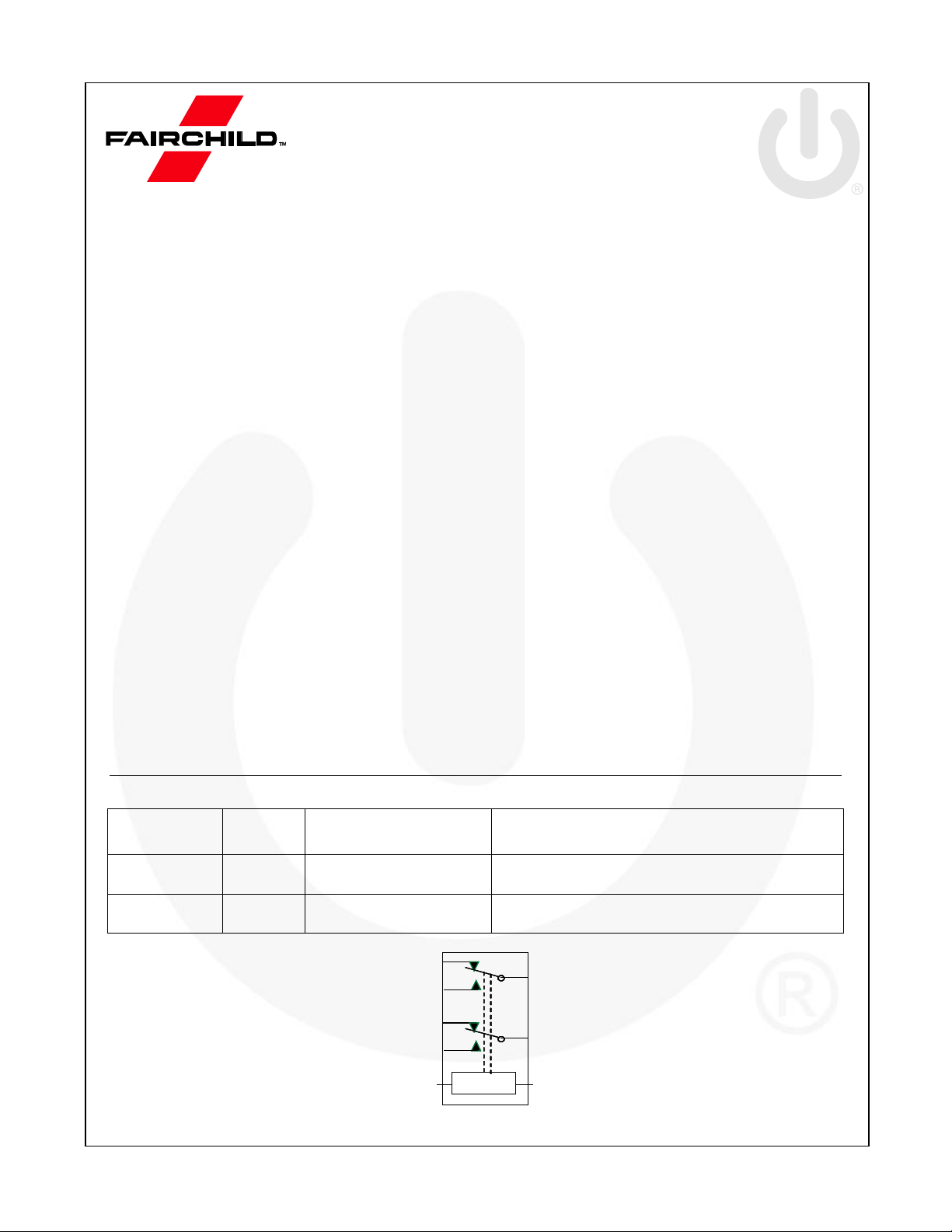
Figure 1. Analog Symbol
Page 2
FSUSB42 — Low-Power, Two-Port, High-Speed, USB2.0 (480Mbps) UART Switch
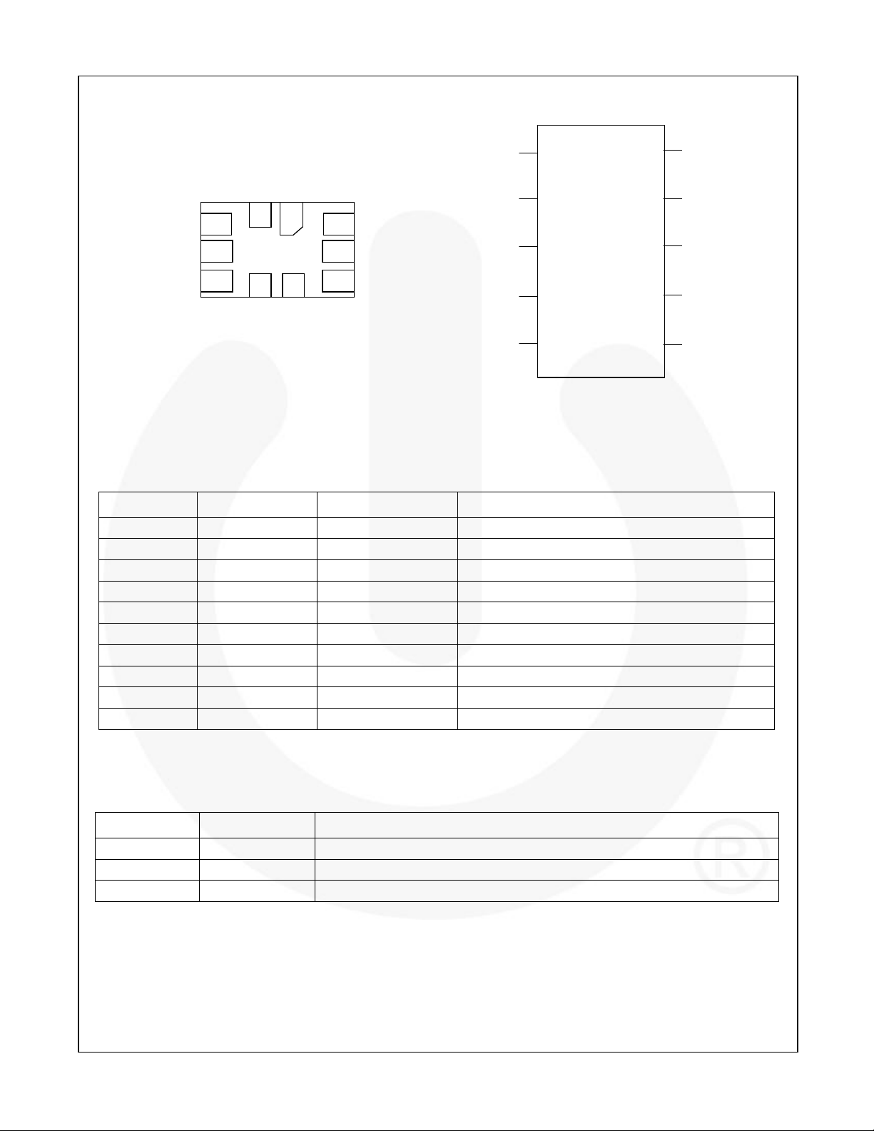
Figure 2. 10-Lead UMLP (Top-Through View)
Figure 3. 10-Lead MSOP (Top-Through View)
UMLP Pin#
MSOP Pin#
Name
Description
1 3 D+
Common USB Data Bus
2 4 D-
Common USB Data Bus
3 5 GND
Ground 4 6
HSD1-
Multiplexed Source Input 1
5 7 HSD1+
Multiplexed Source Input 1
6 8 HSD2-
Multiplexed Source Input 2
7 9 HSD2+
Multiplexed Source Input 2
8
10
/OE
Switch Enable
9 1 VCC
Supply Voltage
10 2 Sel
Switch Select
SEL
/OE
Function
X
HIGH
Disconnect
LOW
LOW
D+= HSD1+, D-= HSD1-
HIGH
LOW
D+= HSD2+, D-= HSD2-
V
cc
GND
1
85
4
3
2
Sel
D+D-
HSD2+HSD2-
HSD1+
/OE
9
10
6 7
HSD1-
5
4
3
2
1
6
7
8
9
10
V
CC
Sel
D+
D-
GND
/OE
HSD1-
HSD2-
HSD1+
HSD2+
Pin Assignments
Pin Definitions
Truth Table
Notes:
1. LOW ≤VIL.
2. HIGH ≥VIH.
3. X=Don’t Care.
© 2007 Fairchild Semiconductor Corporation www.fairchildsemi.com
FSUSB42 • Rev. 1.25 2
Page 3
FSUSB42 — Low-Power, Two-Port, High-Speed, USB2.0 (480Mbps) UART Switch
Symbol
Parameter
Min.
Max.
Unit
VCC
Supply Voltage
-0.5
5.6 V V
CNTRL
DC Input Voltage (S, /OE)
(4)
-0.5
VCC V VSW
DC Switch I/O Voltage
(4)
(VCC=0V)
-0.50
5.25
V
IIK
DC Input Diode Current
-50 mA
I
OUT
DC Output Current
100
mA
T
STG
Storage Temperature
-65
+150
°C
MSL
Moisture Sensitivity Level (JEDEC J-STD-020A)
1 Level
ESD
Human Body Model, JEDEC: JESD22-A114
All Pins
7
kV
I/O to GND
8
Power to GND
16
D+/D- 9
IEC 61000-4-2 System on USB Connector
Pins D+ & D-
Air Discharge
15
Contact
8
Charged Device Model, JEDEC: JESD22-C101
2
Symbol
Parameter
Min.
Max.
Unit
V
CC
Supply Voltage
2.4
4.4
V
V
CNTRL
Control Input Voltage (S, /OE)
(5)
0
VCC
V
V
SW
Switch I/O Voltage
-0.5
4.5 V T
A
Operating Temperature
-40
+85
°C
Absolute Maximum Ratings
Stresses exceeding the absolute maximum ratings may damage the device. The device may not function or be
operable above the recommended operating conditions and stressing the parts to these levels is not recommended.
In addition, extended exposure to stresses above the recommended operating conditions may affect device reliability.
The absolute maximum ratings are stress ratings only.
Note:
4. The input and output negative ratings may be exceeded if the input and output diode current ratings are observed.
Recommended Operating Conditions
The Recommended Operating Conditions table defines the conditions for actual device operation. Recommended
operating conditions are specified to ensure optimal performance to the datasheet specifications. Fairchild does not
recommend exceeding them or designing to Absolute Maximum Ratings.
Note:
5. The control input must be held HIGH or LOW and it must not float.
© 2007 Fairchild Semiconductor Corporation www.fairchildsemi.com
FSUSB42 • Rev. 1.25 3
Page 4
FSUSB42 — Low-Power, Two-Port, High-Speed, USB2.0 (480Mbps) UART Switch
Symbol
Parameter
Condition
VCC (V)
TA=- 40°C to +85°C
Unit
Min.
Typ.
Max.
V
IK
Clamp Diode Voltage
IIN=-18mA
3.0
-1.2
V
V
IH
Input Voltage High
2.4 to 3.6
1.3 V 4.3
1.7
V
IL
Input Voltage Low
2.4 to 3.6
0.5 V 4.3
0.7
I
IN
Control Input Leakage
VSW=0 to VCC
0 to 4.3
-1 1
µA
IOZ
Off State Leakage
0 Dn, HSD1n, HSD2n
3.6 V
4.3
-2 2
µA
I
OFF
Power-Off Leakage Current
(All I/O Ports)
VSW=0 V to 4.3 V, VCC=0 V
Figure 5
0
-2 2
µA
RON
HS Switch On Resistance
(6)
VSW=0.4 V, ION=-8 mA
Figure 4
2.4
4.5
7.5
3.0
3.9
6.5
∆RON
HS Delta R
ON
(7)
VSW=0.4 V, ION=-8 mA
3.0
0.65
ICC
Quiescent Supply Current
V
CNTRL
=0 or VCC, I
OUT
=0
4.3 1 µA
I
CCT
Increase in I
CC
Current per
Control Voltage and VCC
V
CNTRL
=2.6 V, VCC=4.3 V
4.3
10
µA
V
CNTRL
=1.8 V, VCC=4.3 V
4.3
15
µA
DC Electrical Characteristics
All typical value are at TA=25°C unless otherwise specified.
Notes:
6. Measured by the voltage drop between HSDn and Dn pins at the indicated current through the switch.
On resistance is determined by the lower of the voltage on the two (HSDn or Dn ports).
7. Guaranteed by characterization.
© 2007 Fairchild Semiconductor Corporation www.fairchildsemi.com
FSUSB42 • Rev. 1.25 4
Page 5

FSUSB42 — Low-Power, Two-Port, High-Speed, USB2.0 (480Mbps) UART Switch
Symbol
Parameter
Condition
VCC (V)
TA=- 40°C to +85°C
Unit
Min.
Typ.
Max.
tON
Turn-On Time
S, /OE to Output
RL=50 Ω, CL=5 pF, VSW=0.8 V,
Figure 6, Figure 7
2.4 24
40
ns
3.0 to 3.6
13
30
t
OFF
Turn-Off Time
S, /OE to Output
RL=50 Ω, CL=5 pF, VSW=0.8 V,
Figure 6, Figure 7
2.4 15
35
ns
3.0 to 3.6
12
25
t
PD
Propagation Delay8
CL=5 pF, RL=50 Ω, Figure 6,
Figure 8
3.3
0.25
ns
t
BBM
Break-Before-Make
RL=50 Ω, CL=5 pF,
V
SW1=VSW2
=0.8 V, Figure 10
2.4
2.0 10
ns
3.0 to 3.6
2.0 6.5
O
IRR
Off Isolation
RL=50 Ω, f=240 MHz, Figure 12
3.0 to 3.6
-30 dB
Xtalk
Non-Adjacent Channel
Crosstalk
RL=50 Ω, f=240 MHz, Figure 13
3.0 to 3.6
-45 dB
BW
-3db Bandwidth
RL=50 Ω, CL=0 pF, Figure 11
3.0 to 3.6
720
MHz
RL=50 Ω, CL=5 pF, Figure 11
550
MHz
Symbol
Parameter
Condition
VCC (V)
TA=- 40ºC to +85ºC
Unit
Min.
Typ.
Max.
t
SK(P)
Skew of Opposite Transitions of
the Same Output
(9)
CL=5 pF, RL=50 Ω, Figure 9
20 ps
tJ Total Jitter
(9)
RL=50 Ω, CL=5 pF,
tR=tF=500 ps (10-90%) at
480 Mbps (PRBS=215 – 1)
200 ps
Symbol
Parameter
Condition
TA=- 40°C to +85°C
Unit
Min.
Typ.
Max.
C
IN
Control Pin Input Capacitance
VCC=0 V
1.5
pF
C
ON
D+/D- On Capacitance
VCC=3.3 V, /OE=0 V, f=240 MHz,
Figure 15
3.7
C
OFF
D1n, D2n Off Capacitance
VCC and /OE=3.3 V, Figure 14
2.0
AC Electrical Characteristics
All typical value are for VCC=3.3 V at TA=25°C unless otherwise specified.
Note:
8. Guaranteed by characterization.
USB High-Speed-Related AC Electrical Characteristics
All typical value are for VCC=3.3 V at TA=25°C unless otherwise specified.
Note:
9. Guaranteed by characterization.
Capacitance
© 2007 Fairchild Semiconductor Corporation www.fairchildsemi.com
FSUSB42 • Rev. 1.25 5
Page 6

FSUSB42 — Low-Power, Two-Port, High-Speed, USB2.0 (480Mbps) UART Switch
Figure 4. On Resistance
Figure 5. Off Leakage
Figure 6. AC Test Circuit Load
Figure 7. Turn-On / Turn-Off Waveforms
Figure 8. Propagation Delay (tRtF – 500 ps)
Figure 9. Intra-Pair Skew Test t
SK(P)
Select
HSD
n
Dn
V
Sel
= 0 orVcc
I
ON
V
ON
R
ON
= VON/ I
ON
GND
V
SW
GND
SW
Select
V
Sel
= 0 orVcc
NC
A
I
Dn(OFF)
V
SW
GND
V Vcc
**Each switch port is tested separately
RL, RS, and CLare functions of the application
environment (see AC Tables for specific values)
CLincludes test fixture and stray capacitance.
R
L
C
L
HSD
n
Dn
GND
GND
R
S
V
Sel
V
SW
GND
V
OUTVOUT
t
RISE
= 2.5ns
GND
V
CC
90% 90%
10%10%
t
FALL
= 2.5ns
VCC/2
VCC/2
Input– V
/OE
,V
Sel
Output- V
OUT
90%
V
OH
V
OL
t
ON
t
OFF
90%
V
– V
V
–
t
RISE
= 500ps
-400mV
90% 90%
10%10%
t
FALL
= 500ps
0V
Output
t
PHL
+400mV
t
PLH
Test Diagrams
© 2007 Fairchild Semiconductor Corporation www.fairchildsemi.com
FSUSB42 • Rev. 1.25 6
Page 7

FSUSB42 — Low-Power, Two-Port, High-Speed, USB2.0 (480Mbps) UART Switch
Figure 10. Break-Before-Make Interval Timing
Figure 11. Bandwidth
Figure 12. Channel Off Isolation
Figure 13. Non-Adjacent Channel-to-Channel Crosstalk
Capacitance
Meter
HSDn
Dn
S=LOW or HIGH
OE=HIGH
Capacitance
Meter
HSDn
Dn
S=LOW or HIGH
OE=LOW
Figure 14. Channel Off Capacitance
Figure 15. Channel On Capacitance
V
cc
0.9*V
out
Vcc/2
t
BBM
0V
V
OUT
Input - V
Sel
0.9*V
out
t
RISE
= 2.5ns
90%
10%
C
L
HSD
n
R
L
Dn
GND
GND
R
S
V
Sel
V
SW1
GND
V
OUT
V
SW2
GND
--
RL, RS, and CLare functions of the application
environment (see AC Tables for specific values)
CLincludes test fixture and stray capacitance.
V
OUT
GND
GND
R
T
GND
GND
V
S
R
S
Network Analyzer
V
Sel
GND
RSand RTare functions of the application
environment (see AC Tables for specific values).
V
IN
RSand RTare functions of the application
environment (see AC Tables for specific values).
V
OUT
GND
GND
R
T
GND
GND
V
S
R
S
Network Analyzer
R
T
GND
V
Sel
GND
V
IN
R
T
Off isolation = 20 Log (V
OUT
/ VIN)
V
OUT
GND
GND
R
T
GND
GND
V
S
R
S
Network Analyzer
R
T
GND
RSand RTare functions of the application environment
(see AC Tables for specific values).
V
Sel
GND
NC
V
IN
Crosstalk = 20 Log (V
OUT
/ VIN)
Test Diagrams (Continued)
© 2007 Fairchild Semiconductor Corporation www.fairchildsemi.com
FSUSB42 • Rev. 1.25 7
Page 8

FSUSB42 — Low-Power, Two-Port, High-Speed, USB2.0 (480Mbps) UART Switch
A
B
C
SEATING
PLANE
DETAIL A
PIN#1 IDENT
RECOMMENDED
LAND PATTERN
NOTES:
A. PACKAGE DOES NOT CONFORM TO
ANY JEDEC STANDARD.
B. DIMENSIONS ARE IN MILLIMETERS.
C. DIMENSIONS AND TOLERANCES PER
ASME Y14.5M, 2009.
D. LAND PATTERN RECOMMENDATION IS
EXISTING INDUSTRY LAND PATTERN.
E. DRAWING FILENAME: MKT-UMLP10Arev6.
TOP VIEW
BOTTOM VIEW
0.05
C
0.08
C
0.05
C
2X
2X
SIDE VIEW
0.10
C
0.025±.025
3
6
1
0.10
C A B
0.05
C
0.50±.05
10
1.40
1.80
0.40
0.20±.05 (10X)
0.40±.05
(9X)
1.70
2.10
0.40
0.663
0.563
(9X)
0.225
(10X)
1
0.15±.05
1.00±.05
DETAIL A
SCALE : 2X
1.85
1.45
0.55
0.40
0.225
(10X)
9X
0.45
PIN#1 IDENT
OPTIONAL MINIMIAL
TOE LAND PATTERN
SCALE : 2X
LEAD
OPTION 1
SCALE : 2X
LEAD
OPTION 2
PACKAGE
EDGE
45°
0.40±.05
1.40±.05
1.80±.05
(0.20)
4X
(0.60)
4X
Physical Dimensions
Figure 16. 10-Lead, Ultrathin Molded Leadless Package (UMLP)
© 2007 Fairchild Semiconductor Corporation www.fairchildsemi.com
FSUSB42 • Rev. 1.25 8
Page 9

FSUSB42 — Low-Power, Two-Port, High-Speed, USB2.0 (480Mbps) UART Switch
Physical Dimensions (Continued)
Figure 17. 10-Lead, Molded Small Outline Package (MSOP)
© 2007 Fairchild Semiconductor Corporation www.fairchildsemi.com
FSUSB42 • Rev. 1.25 9
Page 10

FSUSB42 — Low-Power, Two-Port, High-Speed, USB2.0 (480Mbps) UART Switch
© 2007 Fairchild Semiconductor Corporation www.fairchildsemi.com
FSUSB42 • Rev. 1.25 10
Page 11

 Loading...