

Page 1
FSTD32450
Configurable 4-Bit to 40-Bit Bus Switch with
Selectable Level Shifting (Preliminary)
Preliminary
FSTD32450 Configurable 4-Bit to 40-Bit Bus Switch with Selectable Level Shifting (Preliminary)
February 2001
Revised August 2001
General Description
The Fairchild Univers al Bus Switch FSTD32450 provides
4-bit, 5-bit, 8-bit, 10 -bit, 16 -bit, 2 0-bit...4 0-bit o f high- speed
CMOS TTL-compatible bus switching. The low On Re sistance of the switch allows inputs to be connect ed to outputs without adding propagation delay or generating
additional ground bounce noise.
The FSTD32450 is designed to allow “customer” configuration control of the en able connections. Th e device can be
organized as eithe r a ten 4-bit, eight 5-bit , four 10-bit, two
20-bit or one 40-bit enable d bus switch. Also achievable
are 8-bit and 16-bit enab led co nfigura tion s (see Fu nctional
Description). The device’s bit configuration is controlled
through select pin logic. (s ee Truth Table). When OE
LOW, Port A
the switch is OPEN.
Another key device feature is the addition of a level shifting
select pin, “S
device behaves as a st andard N-MOS switch. When S
and S5 are HIGH, a diode to VCC is integrated into the circuit allowing for level sh ifting between 5V inputs and 3.3V
outputs.
is connected to Port Bx. When OEx is HIGH,
x
and S5”. When S2 and S5 are LOW, the
2
Features
■ Voltage level shifting
■ 4
Ω switch connection between two ports
■ Minimal propagation delay through the switch
■ Low l
CC
■ Zero bounce in flow-through mode
■ Control inputs compatible with TTL level
■ Packaged in plastic Fine-Pitch Ball Grid Array
(FBGA) (Preliminary)
Applications Note
Select pins S0, S1, S2, S3, S4 and S5 are intended to be
is
x
used as static user confi gurable control pins. The AC p erformance of these pins has not been characterized or
tested. Switching of these select pins during system operation may temporarily disrupt output logic states and/or
enable pin controls.
2
40-bit configuration can be achieved by connecting the
OE
and the OE6 pins to together.
1
Ordering Code:
Order Number Package Number Package Description
FSTD32450GX
(Note 1)
Note 1: BGA package available in Tape and Reel only.
BGA114A
(Preliminary)
114-Ball Fine-Pitch Ball Grid Array (FBGA), JEDEC MO-205, 5.5mm Wide
[Tape and Reel]
UHC is a trademark of Fairchild Semiconductor Corporation.
© 2001 Fairchild Semiconductor Corporation DS500563 www.fairchildsemi.com
Page 2
Preliminary
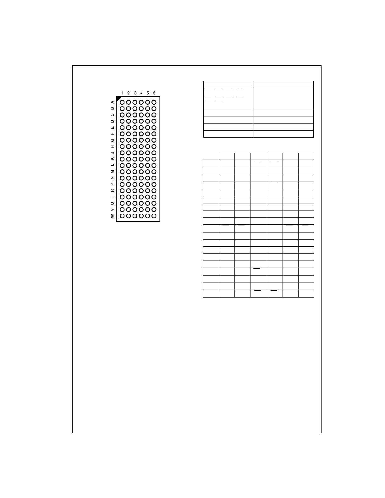
Connection Diagram
Pin Assignment for FBGA
FSTD32450
(Top Thru View)
Pin Descriptions
Pin Name Description
OE
, OE2, OE3, OE4, Bus Switch
1
, OE6, OE7, OE8Enables
OE
5
OE
, OE
9
10
1A, 2A, 3A, 4A Bus A
1B, 2B, 3B, 4B Bus B
, S1, S3, S
S
0
S
, S
2
4
5
Bit Configuration Enables
Level Shifting Diode Enables
FBGA Pin Assignments
123456
A 1A
B 1A61A51A11B11B51B
C 1A81A71A31B31B71B
D 1A101A9GND OE51B91B
E 2A22A1S0V
F 2A42A3S
G 2A62A5VCCGND 2B52B
H 2A82A7GND GND 2B72B
J 2A102A9GND GND 2B92B
K OE4OE8GND GND OE9OE
L 3A103A9GND GND 3B93B
M 3A83A7GND GND 3B73B
N 3A63A5GND V
P 3A43A3S
R 3A23A1V
T 4A104A9OE10GND 4B94B
U 4A84A74A34B34B74B
V 4A64A54A14B14B54B
W 4A44A2OE7OE64B24B
1A2OE1OE21B21B
4
CC
S22B32B
1
CC
S43B33B
5
S33B13B
CC
2B12B
3B53B
4
6
8
10
2
4
6
8
10
3
10
8
6
4
2
10
8
6
4
www.fairchildsemi.com 2
Page 3
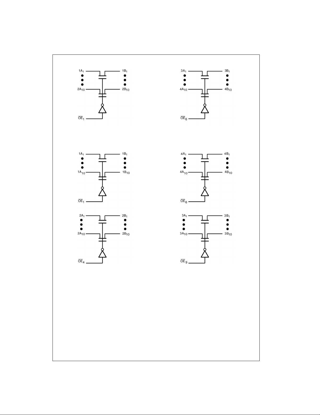
Logic Diagrams
Preliminary
FSTD32450
20-Bit Configuration
10-Bit Configuration
3 www.fairchildsemi.com
Page 4
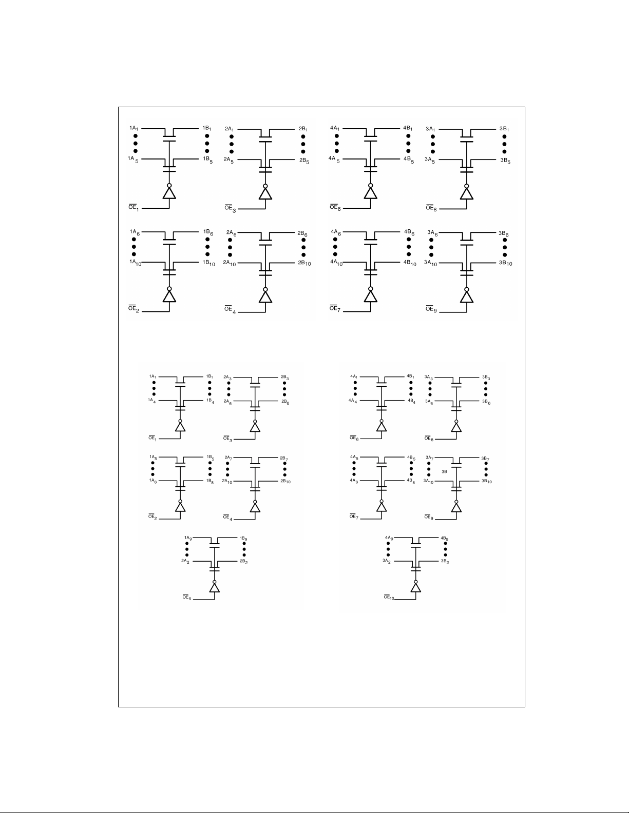
FSTD32450
Preliminary
5-Bit Configuration
4-Bit Configuration
www.fairchildsemi.com 4
Page 5

Preliminary
Functional Description
The device can also be configured as a n 8 and 16-bit device by grounding the unu sed pins in Configurat ions 2 and 1
respectively. The 8-bit configuration may also be achieved by tying two of the 4-bit enables from configuration together and
tying the remaining enable pin (OE
) HIGH.
FSTD32450
Truth Tables (X = V
or GND)
CC
(see Functional Descripti o n)
Select Pin
S
, S
2
5
Mode
L Std. NMOS Switch
H Level Shifting Diode Enabled
20-Bit Configuration (S
OE
1
LXXXX 1A
OE
2
= S1 = L)
0
Inputs
OE
OE
3
OE
4
5
Inputs/Outputs
= 1B
1-10
1-10
, 2A
1-10
HXXXX Z
S
= S4 = L
Inputs
OE
OE
6
7
OE
LXXXX 3A
3
OE
8
OE
9
10
Inputs/Outputs
= 3B
1-10
1-10
, 4A
1-10
HXXXX Z
10-Bit Configuration (S
= L, S1 = H)
0
Inputs Inputs/Outputs
OE
OE
1
2
LXXLX 1A
LXXHX 1A
OE
3
OE
4
OE
1A
5
1-10
= 1B
= 1B
X
= 1B
X
1-10
X
X
2A
HXXLX Z 2A
HXXHX Z Z
= L, S4 = H
S
3
Inputs Inputs/Outputs
OE
LXXLX 4A
LXXHX 4A
OE
6
7
OE
8
OE
OE
9
10
4A
1-10
= 4B
= 4B
X
= 4B
X
1-10
X
X
3A
HXXLX Z 3A
HXXHX Z Z
= 2B
1-10
= 4B
1-10
= 2B
1-10
2AX = 2B
= 2B
X
= 3B
1-10
3AX = 3B
= 3B
X
1-10
X
Z
X
1-10
X
Z
X
5 www.fairchildsemi.com
Page 6

Truth Tables (Continued)
5-Bit Configuration (S
Inputs Inputs/Outputs
OE2OE3OE4OE51A
OE
FSTD32450
1
LLLLX1A
LLLHX1A
LLHLX1A
LLHHX1A
LHLLX1A
LHLHX1A
LHHLX1A
LHHHX1A
HLLLX Z 1A
HLLHX Z 1A
HLHLX Z 1A
HLHHX Z 1A
HHL LX Z Z 2A
HHLHX Z Z 2A
HHHLX Z Z Z 2A
HHHHX Z Z Z Z
Inputs Inputs/Outputs
OE
OE7OE8OE9OE
6
LLLLX4A
LLLHX4A
LLHLX4A
LLHHX4A
LHLLX4A
LHLHX4A
LHHLX4A
LHHHX4A
HLLLX Z 4A
HLLHX Z 4A
HLHLX Z 4A
HLHHX Z 4A
HHL LX Z Z 3A
HHLHX Z Z 3A
HHHLX Z Z Z 3A
HHHHX Z Z Z Z
= H, S1 = L)
0
S
3
= H, S4 = L
Preliminary
, 1B
1-5
= 1B
x
= 1B
x
= 1B
x
= 1B
x
= 1B
x
= 1B
x
= 1B
x
= 1B
x
4A
10
1-5
, 4B
= 4B
x
= 4B
x
= 4B
x
= 4B
x
= 4B
x
= 4B
x
= 4B
x
= 4B
x
1-5
1-5
1A
, 1B
6-10
1Ay = 1B
x
1Ay = 1B
x
1Ay = 1B
x
1Ay = 1B
x
x
x
x
x
x
x
x
x
x
x
x
x
Z2A
Z2A
ZZ2A
ZZZ
= 1B
y
= 1B
y
= 1B
y
= 1B
y
4A
, 4B
6-10
4Ay = 4B
4Ay = 4B
4Ay = 4B
4Ay = 4B
Z3A
Z3A
ZZ3A
ZZZ
= 4B
y
= 4B
y
= 4B
y
= 4B
y
6-10
y
y
y
y
y
y
y
y
6-10
y
y
y
y
y
y
y
y
2A
, 2B
1-5
2Ax = 2B
2Ax = 2B
Z2A
1-5
2A
, 2B
6-10
2Ay = 2B
x
x
Z
= 2B
y
ZZ
= 2B
x
= 2B
x
2Ax = 2B
2Ax = 2B
Z2A
2Ay = 2B
x
x
x
x
Z
= 2B
y
2Ay = 2B
Z
= 2B
y
ZZ
= 2B
x
= 2B
x
3A
, 3B
1-5
3Ax = 3B
3Ax = 3B
Z3A
1-5
2Ay = 2B
x
x
x
x
3A
6-10
3Ay = 3B
Z
= 2B
y
, 3B
Z
= 3B
y
ZZ
= 3B
x
= 3B
x
3Ax = 3B
3Ax = 3B
Z3A
3Ay = 3B
x
x
x
x
Z
= 3B
y
3Ay = 3B
Z
= 3B
y
ZZ
= 3B
x
= 3B
x
3Ay = 3B
x
x
Z
= 3B
y
6-10
y
y
y
y
y
y
y
y
6-10
y
y
y
y
y
y
y
y
www.fairchildsemi.com 6
Page 7

Preliminary
Truth Tables (Continued)
4-Bit Configuration (S
OE2OE3OE4OE51A
OE
1
LLLLL1Ax = 1B
LLLLH1Ax = 1B
LLLHL1A
LLLHH1Ax = 1B
LLHLL1A
LLHLH1Ax = 1B
LLHHL1A
LLHHH1Ax = 1B
LHLLL1A
LHLLH1Ax = 1B
LHLHL1A
LHLHH1Ax = 1B
LHHLL1A
LHHLH1Ax = 1B
LHHHL1A
LHHHH1Ax = 1B
HLLLL Z 1A
HLLLH Z 1Ay = 1B
HLLHL Z 1A
HLLHH Z 1Ay = 1B
HLHLL Z 1A
HLHLH Z 1Ay = 1B
HLHHL Z 1A
HLHHH Z 1Ay = 1B
HHL LL Z Z 2A
HHL LH Z Z 2Ax = 2B
HHLHL Z Z 2A
HHLHH Z Z 2Ax = 2B
HHHL L Z Z Z 2A
HHHLH Z Z Z 2Ay = 2B
HHHHL Z Z Z Z
HHHHH Z Z Z Z Z
= S1 = H)
0
Inputs Inputs/Outputs
1-4
, 1B
= 1B
x
= 1B
x
= 1B
x
= 1B
x
= 1B
x
= 1B
x
= 1B
x
1A
1-4
x
x
x
x
x
x
x
x
x
x
x
x
x
x
x
x
, 1B
5-8
1Ay = 1B
1Ay = 1B
1Ay = 1B
1Ay = 1B
1Ay = 1B
1Ay = 1B
1Ay = 1B
1Ay = 1B
Z2A
Z2A
Z2A
Z2A
ZZ2A
ZZ2A
ZZZ
ZZZZ
= 1B
y
= 1B
y
= 1B
y
= 1B
y
5-8
2A
, 2B
3-6
3-62A7-10
2Ax = 2B
y
y
y
y
y
y
y
y
y
y
y
y
y
y
y
y
x
2Ax = 2B
x
2Ax = 2B
x
2Ax = 2B
x
Z2A
Z2A
ZZ
ZZZ
= 2B
x
x
= 2B
x
x
= 2B
x
x
= 2B
x
x
2Ax = 2B
x
2Ax = 2B
x
2Ax = 2B
x
2Ax = 2B
x
Z2A
Z2A
ZZ
ZZZ
= 2B
x
x
x
= 2B
x
x
x
1A
7-10
y
y
9-10
2A
1Az = 1B
2Az = 2B
1A
2Az = 2B
, 2B
2Ay = 2B
2Ay = 2B
Z
ZZ
= 2B
y
= 2B
y
1Az = 1B
y
2Az = 2B
y
1A
2Az = 2B
2Ay = 2B
2Ay = 2B
Z
1Az = 1B
y
2Az = 2B
y
1A
2Az = 2B
ZZ
= 2B
y
= 2B
y
1Az = 1B
y
2Az = 2B
y
1A
2Az = 2B
2Ay = 2B
2Ay = 2B
Z
1Az = 1B
y
2Az = 2B
y
1A
2Az = 2B
ZZ
= 2B
y
= 2B
y
1Az = 1B
y
2Az = 2B
y
1A
2Az = 2B
2Ay = 2B
2Ay = 2B
Z
1Az = 1B
y
2Az = 2B
y
1A
2Az = 2B
ZZ
= 2B
y
1Az = 1B
y
2Az = 2B
y
1A
2Az = 2B
1-2
, 2B
, 2B
Z
= 1B
z
Z
= 1B
z
Z
= 1B
z
Z
= 1B
z
Z
= 1B
z
Z
= 1B
z
Z
= 1B
z
Z
= 1B
z
9-10
1-2
z
z
z
z
z
z
z
z
z
z
z
z
z
z
z
z
z
z
z
z
z
z
z
z
z
z
z
z
z
z
z
z
FSTD32450
7 www.fairchildsemi.com
Page 8

Truth Tables (Continued)
4-Bit Configuration (continued)
S
= S4 = H
3
FSTD32450
OE
6
LLLLL4Ax = 4B
LLLLH4Ax = 4B
LLLHL4A
LLLHH4Ax = 4B
LLHLL4A
LLHLH4Ax = 4B
LLHHL4A
LLHHH4Ax = 4B
LHLLL4A
LHLLH4Ax = 4B
LHLHL4A
LHLHH4Ax = 4B
LHHLL4A
LHHLH4Ax = 4B
LHHHL4A
LHHHH4Ax = 4B
HLLLL Z 4A
HLLLH Z 4Ay = 4B
HLLHL Z 4A
HLLHH Z 4Ay = 4B
HLHLL Z 4A
HLHLH Z 4Ay = 4B
HLHHL Z 4A
HLHHH Z 4Ay = 4B
HHL LL Z Z 3A
HHL LH Z Z 3Ax = 3B
HHLHL Z Z 3A
HHLHH Z Z 3Ax = 3B
HHHL L Z Z Z 3A
HHHLH Z Z Z 3Ay = 3B
HHHHL Z Z Z Z
HHHHH Z Z Z Z Z
Inputs Inputs/Outputs
OE7OE8OE9OE104A
1-4
, 4B
= 4B
x
= 4B
x
= 4B
x
= 4B
x
= 4B
x
= 4B
x
= 4B
x
1-4
4A
, 4B
5-8
5-8
4Ay = 4B
x
x
x
x
x
x
x
x
x
x
x
x
x
x
x
x
y
4Ay = 4B
y
4Ay = 4B
y
4Ay = 4B
y
4Ay = 4B
y
4Ay = 4B
y
4Ay = 4B
y
4Ay = 4B
y
Z3A
Z3A
Z3A
Z3A
ZZ3A
ZZ3A
ZZZ
ZZZZ
= 4B
y
y
y
= 4B
y
y
y
= 4B
y
y
y
= 4B
y
y
y
3A
, 3B
3-6
3-63A7-10
3Ax = 3B
x
3Ax = 3B
x
3Ax = 3B
x
3Ax = 3B
x
Z3A
Z3A
, 3B
7-10
3Ay = 3B
y
3Ay = 3B
y
Z
ZZ
= 3B
y
y
= 3B
y
y
ZZ
ZZZ
= 3B
x
= 3B
x
= 3B
x
= 3B
x
3Ax = 3B
3Ax = 3B
3Ax = 3B
3Ax = 3B
Z3A
Z3A
3Ay = 3B
x
x
x
x
x
x
x
x
y
3Ay = 3B
y
Z
ZZ
= 3B
y
y
= 3B
y
y
3Ay = 3B
y
3Ay = 3B
y
Z
ZZ
= 3B
y
y
= 3B
y
y
ZZ
ZZZ
= 3B
x
= 3B
x
3Ay = 3B
x
x
x
x
y
3Ay = 3B
y
Z
ZZ
= 3B
y
y
y
Preliminary
3A
, 3B
1-2
1-2
4A
, 3B
9-10
9-10
3Az = 3B
z
4Az = 4B
z
Z
= 3B
3A
z
z
4Az = 4B
z
3Az = 3B
z
4Az = 4B
z
Z
= 3B
3A
z
z
4Az = 4B
z
3Az = 3B
z
4Az = 4B
z
Z
3A
= 3B
z
z
4Az = 4B
z
3Az = 3B
z
4Az = 4B
z
Z
3A
= 3B
z
z
4Az = 4B
z
3Az = 3B
z
4Az = 4B
z
Z
3A
= 3B
z
z
4Az = 4B
z
3Az = 3B
z
4Az = 4B
z
Z
= 3B
3A
z
z
4Az = 4B
z
3Az = 3B
z
4Az = 4B
z
Z
= 3B
3A
z
z
4Az = 4B
z
3Az = 3B
z
4Az = 4B
z
Z
3A
= 3B
z
z
4Az = 4B
z
www.fairchildsemi.com 8
Page 9

Preliminary
Absolute Maximum Ratings(Note 2) Recommended Operating
Supply Voltage (VCC) −0.5V to +7.0V
DC Switch Voltage (V
) (Note 3) −2.0V to +7.0V
S
DC Input Control Pin Voltage
(V
) (Note 4) −0.5V to +7.0V
IN
DC Input Diode Current (l
DC Output (I
DC V
CC
) Current 128 mA
OUT
/GND Current (ICC/I
Storage Temperature Range (T
) V
< 0V −50 mA
IK
IN
) +/− 100 mA
GND
) −65°C to +150 °C
STG
Conditions
Power Supply Operating (V
Input Voltage (V
Output Voltage (V
Free Air Operating Temperature (T
Note 2: The “Absolute Maximum Ratings” are those value s beyond which
the safety of the d evice cannot b e guaranteed . The device sh ould not be
operated at these limit s. The parametric values defi ned in the Electrical
Characteristics tables are not guaranteed at the absolute maximum rating.
The “Recomm ended O peratin g Cond itions ” table will defin e the condition s
for actual device operation.
is the volt age observed/applied at either the A or B Ports a c ross
Note 3: V
S
the switch.
Note 4: The input and output negative voltage ratings may be exceeded if
the input and ou t put diode current ratings ar e observed.
Note 5: Unused control inputs must be held HIGH or LOW. They may not
float.
(Note 5)
CC)
) 0V to 5.5V
IN
) 0V to 5.5V
OUT
)-40 °C to +85 °C
A
4.0V to 5.5V
DC Electrical Characteristics
Symbol Parameter
V
Clamp Diode Voltage 4.5 −1.2 V IIN = −18mA
IK
V
HIGH Level Input Voltage 4.0-5.5 2.0 V IF S2 = HIGH 4.5V ≤ VCC ≤ 5.5V
IH
LOW Level Input Voltage 4.0-5.5 0.8 V IF S2 = HIGH 4.5V ≤ VCC ≤ 5.5V
V
IL
V
HIGH Level Output Voltage 4.5-5.5 See Figure 3 V S2 = S5 = V
OH
I
Input Leakage Current 5.5 ±1.0 µA0 ≤ VIN ≤ 5.5V
I
I
OFF-STATE Leakage Current 5.5 ±1.0 µA0 ≤ A, B ≤ V
OZ
R
Switch On Resistance 4.5 4 7 Ω VIN = 0V, IIN = 64 mA, S2 = S5 = 0V or V
ON
(Note 7) 4.5 4 7 Ω VIN = 0V, IIN = 30 mA, S2 = S5 = 0V or V
I
Quiescent Supply Current
CC
∆ I
Increase in I
CC
Note 6: Typical values are at VCC = 5.0V and TA = +25°C
Note 7: Measured by the voltage drop between A and B pins at the indicated c urrent through the switch. On Resistanc e is determined by the lower of the
voltages on the two (A or B) pins.
CC
per Input
V
TA = −40 °C to +85 °C
CC
(V) Min
010µAV
4.5 8 12 Ω VIN = 2.4V, IIN = 15 mA, S2 = S5 = 0V
4.0 11 20 Ω V
4.5 35 50 Ω V
5.5
5.5
Typ
(Note 6)
Units Conditions
Max
CC
= 5.5V
IN
CC
= 2.4V, IIN = 15 mA, S2 = S5 = 0V
IN
= 2.4V, IIN = 15 mA, S2 = S5 = V
3 µAS2 = S5 = GND, VIN = VCC or GND, I
10 µAS2 = S5 = VCC, OEx = VCC, VIN = VCC or GND, I
1.5 mA S2 = S5 = VCC, OEx = GND, VIN = VCC or GND, I
2.5 mA
4.0 mA
IN
One Input at 3.4V
Other Inputs at VCC or GND, S2 = 0V
One Input at 3.4V
Other Inputs at VCC or GND, S2 = V
CC
CC
OUT
CC
CC
= 0
OUT
OUT
FSTD32450
= 0
= 0
9 www.fairchildsemi.com
Page 10

Preliminary
AC Electrical Characteristics
= −40 °C to +85 °C,
T
A
C
= 50pF, RU = RD = 500Ω
Symbol Parameter
FSTD32450
t
, t
PHL
t
PZH
t
PHZ
t
PZH
t
PHZ
Note 8: This parameter is guaranteed by design but is not tested. The bus switch contributes no propagation delay other than the RC delay of the typical On
Resistance of the s witch and the 50pF load capacitance, wh en driven by an ideal volt age source (zero output impedance).
Propagation Delay Bus-to-Bus
PLH
(Note 8)
, t
Output Enable Time 1.5 6.5 7.0 ns VI = 7V for t
PZL
, t
Output Disable Time 1.5 6.7 7.2 ns VI = 7V for t
PLZ
, t
, t
PZLSel
PLZSel
(S
) to Output Enable Time 1.5 7.0 7.5 ns VI = 7V for t
0, 1
(S
) to Output Disable Time 1.5 7.5 7.7 ns VI = 7V for t
0, 1
L
= 4.5 – 5.5V VCC = 4.0V (S2 = S5 = 0V)
V
CC
Min Max Min Max
0.25 0.25 ns VI = OPEN Figures
Units
Conditions Figure
= OPEN for t
I
= OPEN for t
I
PZL
PZH
PLZ
PHZ
PZL
PZH
PLZ
PHZ
VI = OPEN for t
VI = OPEN for t
V
V
AC Electrical Characteristics: Translating Diode
T
= −40 °C to +85 °C,
A
= 50pF, RU = RD = 500Ω
C
Symbol Parameter
L
VCC = 4.5 – 5.5V (S2 = S5 = VCC)
Units
Min Max
t
, t
Propagation Delay Bus-to-Bus (Note 9) 0.25 ns VI = OPEN Figures
PLH
, t
Output Enable Time 1.5 10.0 ns VI = 7V for t
PZL
t
PHL
PZH
VI = OPEN for t
t
, t
PHZ
Output Disable Time 1.5 9.0 ns VI = 7V for t
PLZ
VI = OPEN for t
t
PZH
, t
PZLSel
(S
) to Output Enable Time 1.5 11.0 ns VI = 7V for t
0, 1
VI = OPEN for t
t
PHZ
, t
PLZSel
(S
) to Output Disable Time 1.5 10.0 ns VI = 7V for t
0, 1
V
Note 9: This parameter is guaranteed by design but is not tested. This bus switch contributes no propagation delay other than the RC delay of the typical On
Resistance of the s witch and the 50pF load capacitance, wh en driven by an ideal volt age source (zero output impedance).
Conditions Figure
PZL
PZH
PLZ
PHZ
PZL
PZH
PLZ
= OPEN for t
I
PHZ
Number
1, 2
Figures
1, 2
Figures
1, 2
Figures
1, 2
Figures
1, 2
Number
1, 2
Figures
1, 2
Figures
1, 2
Figures
1, 2
Figures
1, 2
Capacitance (Note 10)
Symbol Parameter Typ Max Units Conditions
C
IN
C
I/O
Note 10: TA = +25°C, f = 1 MHz, Capac it ance is characterize d but not tested.
www.fairchildsemi.com 10
Control Pin Input Capacitance 4 pF VCC = 5.0V, VIN = 0V
Input/Output Capacitance “OFF State” 8pFV
, OE = 5.0V, VIN = 0V
CC
Page 11

AC Loading and Waveforms
Note: Input driven by 50Ω source terminated in 50 Ω
includes load and stray capacitance
Note: C
L
Note: Input Frequency = 1.0 MHz, t
FIGURE 1. AC Test Circuit
= 500 ns
W
Preliminary
FSTD32450
FIGURE 2. AC Waveforms
11 www.fairchildsemi.com
Page 12

FSTD32450
Preliminary
FIGURE 3.
www.fairchildsemi.com 12
Page 13

Physical Dimensions inches (millimeters) unless otherwise noted
Preliminary
FSTD32450 Configurable 4-Bit to 40-Bit Bus Switch with Selectable Level Shifting (Preliminary)
114-Ball Fine-Pitch Ball Grid Array (FBGA), JEDEC MO-205, 5.5mm Wide
Package Number BGA114A
Preliminary
Technology Description
The Fairchild Switch family derives from and embodies Fairchild’s proven switch t echnology used for several years in it s
74LVX3L384 (FST3384) bus switch product.
Fairchild does not assume any responsibility for use of any circuitry described , no circuit patent licenses are implied and
Fairchild reserves the right at any time without notice to change said circuitry and specifications.
LIFE SUPPORT POLICY
FAIRCHILD’S PRODUCTS ARE NOT AUTHORIZED FOR USE AS CRITICAL COMPONENTS IN LIFE SUPPORT
DEVICES OR SYSTEMS WITHOUT THE EXPRESS WRITTEN APPROVAL OF THE PRESIDENT OF FAIRCHILD
SEMICONDUCTOR CORPORATION. As used herein:
1. Life support devices or systems are dev ic es or syste ms
which, (a) are intended for surgical implant into the
body, or (b) support or sustain life, and (c) whose failure
to perform when properly used in accordance with
instructions for use provide d in the l abe ling, can be reasonably expected to result in a significant injury to the
user.
2. A critical compo nent in any com ponen t of a life s upp ort
device or system whose failure to perform can be reasonably expected to cause the failure of the life support
device or system, or to affect its safety or effectiveness.
www.fairchildsemi.com
13 www.fairchildsemi.com
 Loading...