

Page 1
April 2013
FDZ8040L — Integrated Load Switch
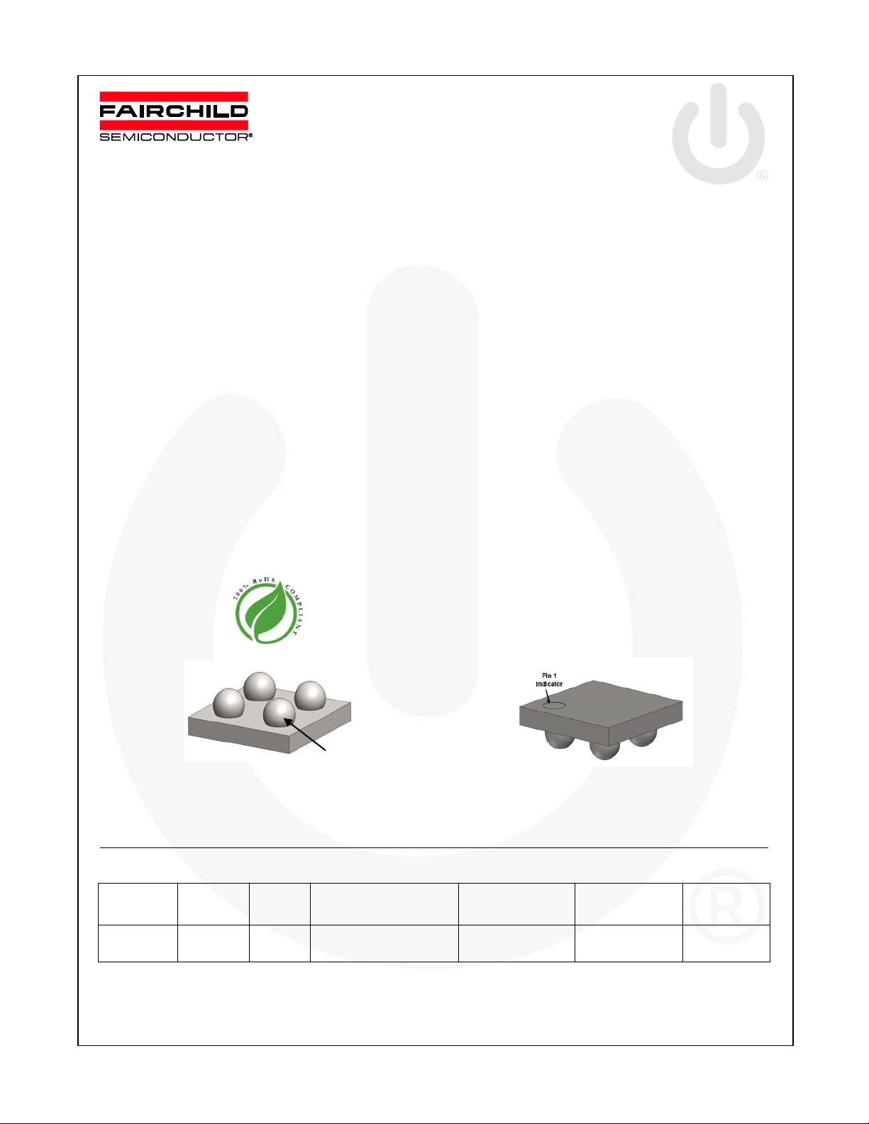
Figure 1. Bottom View
Figure 2. Top View
Part
Number
Device
Mark
Ball
Pitch
Operating
Temperature Range
Switch
Package
Packing
Method
FDZ8040L
ZM
0.4 mm
-40 to 85°C
80 m, P-Channel
MOSFET
0.8 x 0.8 x
0.5 mm3 WLCSP
Tape & Reel
Pin 1
VOUT
GND
ON
VIN
FDZ8040L
Integrated Load Switch
Features
Optimized for Low-Voltage Core ICs in
Portable Systems
Very Small Package Dimension: WLCSP
0.8 X 0.8 X 0.5 mm3
Current = 1.2 A, V
Current = 2 A, V
R
R
R
R
R
= 80 mΩ at VON = VIN = 4 V
DS(on)
= 85 mΩ at VON = VIN = 3.6 V
DS(on)
= 90 mΩ at VON = VIN = 3 V
DS(on)
= 360 mΩ at VON = VIN = 0.9 V
DS(on)
= 1000 mΩ at VON = VIN = 0.8 V
DS(on)
Max. = 4 V
IN
Max. = 4 V (Pulsed)
IN
RoHS Compliant
Description
This device is particularly suited for compact power
management in portable applications needing 0.8 V to
4 V input and 1.2 A output current capability. This load
switch integrated a level-shifting function that drives a Pchannel power MOSFET in a very small 0.8 X 0.8 X
0.5 mm3 WLCSP package.
Applications
Load Switch
Power Management in Portable Applications
Ordering Information
© 2011 Fairchild Semiconductor Corporation www.fairchildsemi.com
FDZ8040L • Rev. C1
Page 2
FDZ8040L — Integrated Load Switch
OFF
ON
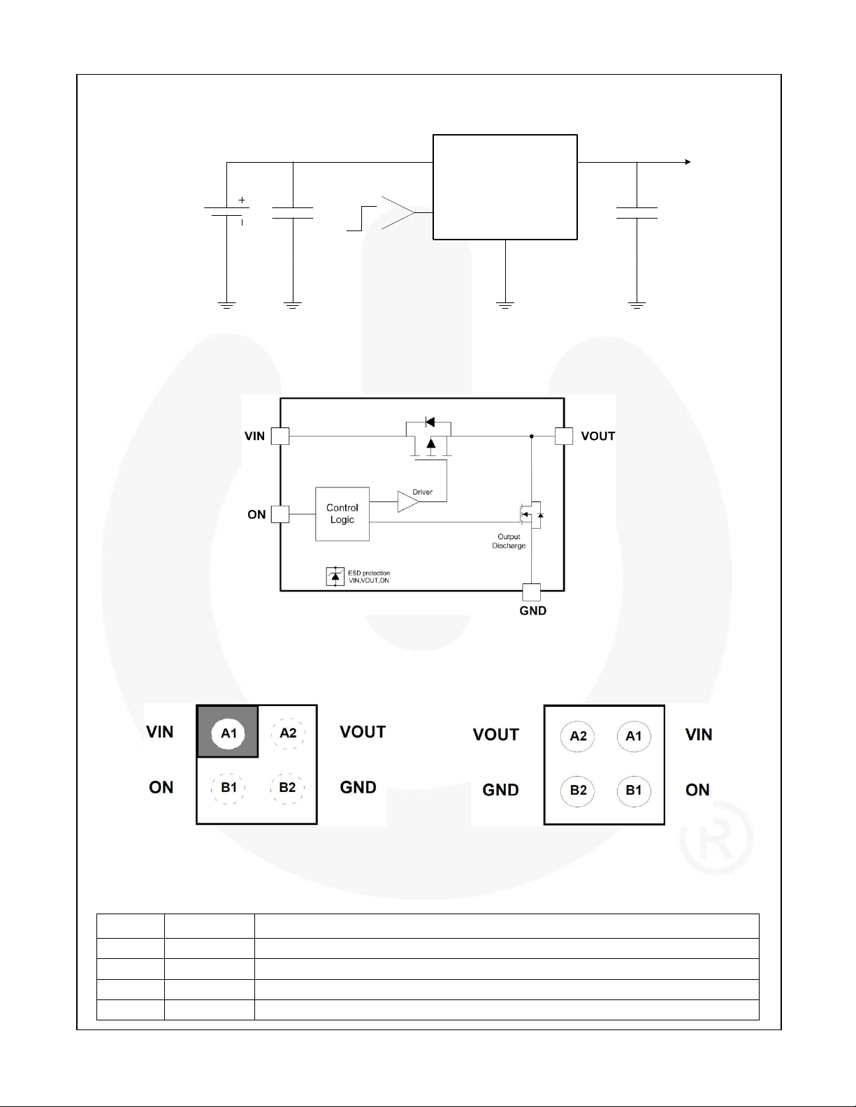
VIN
VOUT
ON
GND
VIN = 0.8 -4 V C
IN
C
OUT
FDZ8040L
Figure 5. Top View (Bumps Down)
Figure 6. Bottom View (Bumps Up)
Pin #
Name
Description
A1
VIN
Supply Input: Input to the load switch
A2
VOUT
Switch Output: Output of the load switch
B1
ON
ON/OFF Control Input
B2
GND
Ground
Typical Application
Figure 3. Typical Application
Block Diagram
Pin Configuration
Pin Descriptions
© 2011 Fairchild Semiconductor Corporation www.fairchildsemi.com
FDZ8040L • Rev. C6 2
Figure 4. Internal Block Diagram
Page 3
FDZ8040L — Integrated Load Switch
Symbol
Parameter
Min.
Max.
Unit
VIN
Voltage on VIN, VOUT, ON to GND
-0.3
4.2
V
I
OUT_C
I
OUT
-Load Current (Continuous)
(1a)
1.2
A
I
OUT_P
I
OUT
-Load Current (Pulsed)
2 A
PD
Power Dissipation at TA = 25°C
(1a)
0.9
W
TA
Operating Temperature Range
-40
85
°C
T
STG
Storage Temperature
-65
150
°C
R
ΘJA
Thermal Resistance, Junction to Ambient
(1a)
135
°C/W
ESD
Electrostatic Discharge Capability
Human Body Model, JESD22-A114
8
kV
Charged Device Model, JESD22-C101
2
a. 135°C/W when mounted on a
1-inch square pad of 2-oz copper.
b. 360°C/W when mounted on a
minimum pad of 2-oz copper.
Symbol
Parameter
Min.
Max.
Unit
VIN
Voltage on VIN Pin
0.8
4.0
V
VON
Voltage on ON Pin
0.7
4.0
V
TA
Operating Temperature
Range
1 V to 4 V
-40
85
°C
0.8 V to 4 V
-10
Absolute Maximum Ratings
Stresses exceeding the absolute maximum ratings may damage the device. The device may not function or be
operable above the recommended operating conditions and stressing the parts to these levels is not recommended.
In addition, extended exposure to stresses above the recommended operating conditions may affect device reliability.
The absolute maximum ratings are stress ratings only.
Notes:
1. RΘJA is the sum of the junction-to-case and case-to-ambient thermal resistance where the case thermal
reference is defined as the solder mounting surface of the drain pins. RΘJC is guaranteed by design, while RΘJA
is determined by the board design.
2. Pulse test: pulse width < 300 µs; duty cycle < 2.0%.
Recommended Operating Conditions
The Recommended Operating Conditions table defines the conditions for actual device operation. Recommended
operating conditions are specified to ensure optimal performance to the datasheet specifications. Fairchild does not
recommend exceeding them or designing to Absolute Maximum Ratings.
© 2011 Fairchild Semiconductor Corporation www.fairchildsemi.com
FDZ8040L • Rev. C6 3
Page 4
FDZ8040L — Integrated Load Switch
Symbol
Parameter
Test Conditions
Min.
Typ.
Max.
Unit
VIN
Operation Voltage
0.8 4.0
V
VIL
ON Input Logic Low Voltage
1.6 V ≤ VIN ≤ 4.0 V
0.35
V
0.8 V ≤ VIN ≤ 1.6 V
0.25
VIH
ON Input Logic High Voltage
1.6 V ≤ VIN ≤ 4.0 V
1.0
V
0.8 V ≤ VIN ≤ 1.6 V
0.7
IQ
Quiescent Current
I
OUT
= 0 mA, VIN = VON = 1.8 V
2.1
μA
I
Q(off)
Off Supply Current
I
OUT
= 0 mA, VIN = 1.8 V, VON = GND
1
μA
I
SD(off)
Off Switch Current
VON = GND, V
OUT
= 0 V, VIN = 1.8 V
100
nA
ION
ON Input Leakage
VON = VIN or GND
1
μA
RPD
Output Discharge Pull-Down
Resistance
200 Ω
R
DS(ON)
Static Drain-Source
On-Resistance
VON = VIN = 4 V, I
OUT
= 300 mA
50
80
mΩ
VON = VIN = 3.6 V, I
OUT
= 300 mA
51
85
VON = VIN = 3 V, I
OUT
= 300 mA
54
90
V
ON
= 0.7 V, V
IN
= 1.6 V, I
OUT
= 300 mA
73
110
V
ON
= 0.7 V, V
IN
= 1 V, I
OUT
= 300 mA
140
309
V
ON
= V
IN
= 0.9 V, I
OUT
= 10 mA
186
360
V
ON
= V
IN
= 0.8 V, I
OUT
= 10 mA
348
1000
V
ON
= V
IN
= 0.9 V, I
OUT
= 10 mA,
T
J
= 10 ~ 85°C
194
370
V
ON
= V
IN
= 0.8 V, I
OUT
= 10 mA,
T
J
= 10 ~ 85°C
268
750
V
IN
= 3.6 V, I
OUT
= 300 mA, T
J
= 85°C
59
102
Electrical Characteristics
TJ = 25°C and VIN=1.8 V, unless otherwise noted.
© 2011 Fairchild Semiconductor Corporation www.fairchildsemi.com
FDZ8040L • Rev. C6 4
Page 5

FDZ8040L — Integrated Load Switch
Symbol
Parameter
Test Conditions
Typical
Unit
t
d(on)
Turn-On Delay Time
V
IN
= 1.6 V, V
ON
= 0.7 V, C
L
= 1 μF, R
L
= 500 Ω
22
μs
tr
Turn-On Rise Time
23
μs
t
d(off)
Turn-Off Delay Time
109
μs
tf
Turn-Off Fall Time
285
μs
t
d(on)
Turn-On Delay Time
V
IN
= 1 V, V
ON
= 1.8 V, C
L
= 1 μF, R
L
= 500 Ω
37
μs
tr
Turn-On Rise Time
35
μs
t
d(off)
Turn-Off Delay Time
112
μs
tf
Turn-Off Fall Time
332
μs
t
d(on)
Turn-On Delay Time
V
IN
= 1.8 V, V
ON
= 1.8 V, C
L
= 1 μF, R
L
= 500 Ω
20
μs
tr
Turn-On Rise Time
22
μs
t
d(off)
Turn-Off Delay Time
122
μs
tf
Turn-Off Fall Time
296
μs
t
d(on)
Turn-On Delay Time
V
IN
= 2.5 V, V
ON
= 1.8 V, C
L
= 1 μF, R
L
= 500 Ω
15
μs
tr
Turn-On Rise Time
19
μs
t
d(off)
Turn-Off Delay Time
160
μs
tf
Turn-Off Fall Time
295
μs
t
d(on)
Turn-On Delay Time
V
IN
= 3.3 V, V
ON
= 1.8 V, C
L
= 1 μF, R
L
= 500 Ω
13
μs
tr
Turn-On Rise Time
18
μs
t
d(off)
Turn-Off Delay Time
193
μs
tf
Turn-Off Fall Time
305
μs
t
d(on)
Turn-On Delay Time
V
IN
= 0.8 V, V
ON
= 0.8 V, C
L
= 1 μF, R
L
= 500 Ω
53
μs
tr
Turn-On Rise Time
56
μs
t
d(off)
Turn-Off Delay Time
143
μs
tf
Turn-Off Fall Time
532
μs
t
d(on)
Turn-On Delay Time
V
IN
= 0.9 V, V
ON
= 0.9 V, C
L
= 1 μF, R
L
= 500 Ω
51
μs
tr
Turn-On Rise Time
54
μs
t
d(off)
Turn-Off Delay Time
148
μs
tf
Turn-Off Fall Time
525
μs
Switching Characteristics
© 2011 Fairchild Semiconductor Corporation www.fairchildsemi.com
FDZ8040L • Rev. C6 5
Page 6

FDZ8040L — Integrated Load Switch
Typical Performance Characteristics
Figure 7. Shutdown Current vs. Temperature
Figure 8. Shutdown Current vs. Supply Voltage
Figure 9. Off Supply Current vs. Temperature
Figure 10. Off Supply Current vs. Supply Voltage
Figure 11. Quiescent Current vs. Temperature
Figure 12. Quiescent Current vs. Supply Voltage
© 2011 Fairchild Semiconductor Corporation www.fairchildsemi.com
FDZ8040L • Rev. C6 6
Page 7

FDZ8040L — Integrated Load Switch
Typical Performance Characteristics
Figure 13. RON vs. Temperature
Figure 14. RON vs. Supply Voltage
Figure 15. ON-Pin Threshold vs. VIN
Figure 16. V
OUT
Rise and Fall Time vs.
Temperature at RL=500
Figure 17. V
OUT
Turn-On and Turn-Off Delay vs.
Temperature at RL=500
Figure 18. Forward Bias Safe Operation Area
© 2011 Fairchild Semiconductor Corporation www.fairchildsemi.com
FDZ8040L • Rev. C6 7
Page 8

FDZ8040L — Integrated Load Switch
Typical Performance Characteristics
Figure 19. Turn-On Response (VIN = 3.3 V, C
OUT
=1 µF, RL=500 Ω)
Figure 20. Turn-Off Response (VIN = 3.3 V, C
OUT
=1 µF, RL=500 Ω)
© 2011 Fairchild Semiconductor Corporation www.fairchildsemi.com
FDZ8040L • Rev. C6 8
Page 9

FDZ8040L — Integrated Load Switch
OFF
ON
VIN
VOUT
ON
GND
VIN = 0.8 -4 V C
IN
C
OUT
FDZ8040L
R
L
Functional Description
The FDZ8040L is a low-R
packaged in space-saving 0.8 x 0.8 WLCSP.
The core of the device is an 80 mΩ P-channel MOSFET
capable of functioning over a wide input operating range
P-channel load switch
DS(ON)
of 0.8-4 V. The ON pin, an active HIGH TTL-compatible
input that supports input as low as 0.7 V, controls the
state of the switch.
Applications Information
Figure 21. Typical Application
Input Capacitor
To reduce device inrush current effect, a 0.1 µF ceramic
capacitor, CIN, is recommended close to the VIN pin. A
higher value of CIN can be used to further reduce the
voltage drop experienced as the switch is turned on into
a large capacitive load.
Output Capacitor
FDZ8040L works without an output capacitor. However,
if parasitic board inductance forces V
when switching off, a 0.1 µF capacitor, C
placed between the VOUT and GND pins.
below GND
OUT
, should be
OUT
© 2011 Fairchild Semiconductor Corporation www.fairchildsemi.com
FDZ8040L • Rev. C6 9
Page 10

FDZ8040L — Integrated Load Switch
Product
D E X
Y
FDZ8040L
0.8 ±0.03 mm
0.8 ±0.03 mm
0.21 mm
0.21 mm
BOTTOM VIEW
SIDE VIEWS
TOP VIEW
RECOMMENDED LAND PATTERN
BALL A1
INDEX AREA
A1
0.005 C A B
F
(NSMD PAD TYPE)
B
A
0.292±0.018
0.208±0.021
NOTES:
A. NO JEDEC REGISTRATION APPLIES.
B. DIMENSIONS ARE IN MILLIMETERS.
C. DIMENSIONS AND TOLERANCE
PER ASME Y14.5M, 1994.
D. DATUM C IS DEFINED BY THE SPHERICAL
CROWNS OF THE BALLS.
E. PACKAGE NOMINAL HEIGHT IS 500 MICRONS
±39 MICRONS (461-539 MICRONS).
F. FOR DIMENSIONS D, E, X, AND Y SEE
PRODUCT DATASHEET.
G. DRAWING FILNAME: MKT-UC004AFrev1.
0.03
C
2X
0.03
C
2X
1
2
A
B
0.40
0.40
(X)±0.018
SEATING PLANE
C
0.06
C
0.05
C
E
D
D
E
0.40
0.40
Ø0.20
Cu Pad
Ø0.30
Solder Mask
(Y)±0.018
Ø0.260±0.020
4X
0.539
0.461
F
Physical Dimensions
Figure 22. 4-Ball, WLCSP, 2 X 2 Array, 0.4 mm Pitch, 250 µm Ball
Product-Specific Dimensions
Package drawings are provided as a service to customers considering Fairchild components. Drawings may change in any manner
without notice. Please note the revision and/or date on the drawing and contact a Fairchild Semiconductor representative to verify or
obtain the most recent revision. Package specifications do not expand the terms of Fairchild’s worldwide terms and conditions, specifically the
warranty therein, which covers Fairchild products.
Always visit Fairchild Semiconductor’s online packaging area for the most recent package drawings:
http://www.fairchildsemi.com/packaging/.
© 2011 Fairchild Semiconductor Corporation www.fairchildsemi.com
FDZ8040L • Rev. C6 10
Page 11

FDZ8040L — Integrated Load Switch
© 2011 Fairchild Semiconductor Corporation www.fairchildsemi.com
FDZ8040L • Rev. C6 11
Page 12

 Loading...