

Page 1

User Guide for
FEB-L032 Evaluation Board
2.7W LED Ballast Using FLS0116
Featured Fairchild Product:
FLS0116
Direct questions or comments
about this evaluation board to:
“Worldwide Direct Support”
Fairchild Semiconductor.com
© 2012 Fairchild Semiconductor Corporation 1 FEB-L032_FLS0116 • Rev. 1.0.1
Page 2

Table of Contents
1. Introduction ............................................................................................................................... 3
1.1. General Description ......................................................................................................... 3
1.2. Key Features .................................................................................................................... 3
1.3. Internal Block Diagram .................................................................................................... 4
2. General Specifications for Evaluation Board ........................................................................... 5
2.1. Photographs of Evaluation Board .................................................................................... 6
2.2. Printed Circuit Board ....................................................................................................... 7
2.3. Schematic ......................................................................................................................... 8
2.4. Bill Of Materials .............................................................................................................. 8
3. Performance of Evaluation Board ............................................................................................. 9
3.1. Typical Waveforms: Startup .......................................................................................... 10
3.2. Operating Frequency & Minimum Duty ........................................................................ 11
3.3. Typical Waveforms: Steady State .................................................................................. 12
3.4. Typical Operating Waveforms: Output Characteristics ................................................. 13
3.5. Typical Waveforms: Abnormal Mode (LED Open) ...................................................... 15
3.6. Typical Waveforms: Abnormal Mode (Inductor Short) ................................................ 16
3.7. System Efficiency .......................................................................................................... 17
3.8. Power Factor at Rated Load Condition .......................................................................... 18
3.9. Total Harmonic Distortion ............................................................................................. 19
3.10. Thermal Performance ..................................................................................................... 20
3.11. EMI Test Results............................................................................................................ 22
4. Revision History ..................................................................................................................... 24
© 2012 Fairchild Semiconductor Corporation 2 FEB-L032_FLS0116 • Rev. 1.0.1
Page 3

This user guide supports the evaluation kit for the FLS0116. It should be used in
conjunction with the FLS0116 datasheet as well as Fairchild’s application notes and
technical support team. Please visit Fairchild’s website at www.fairchildsemi.com
1. Introduction
This document describes the proposed solution for an universal input, 2.7W LED ballast
using the FLS0116. The input voltage range is 90V
output with a constant current of 97mA at 28V
description of FLS0116, the power supply specification, schematic, bill of materials and
the typical operating characteristics.
1.1. General Description
The FLS0116 LED lamp driver is a simple IC with PFC function and integrated
switching MOSFET. The special “adopted digital” technique automatically detects input
voltage condition and sends an internal reference signal, resulting in high power factor
(PF). When AC input voltage is applied to the IC, PFC function is automatically enabled.
When DC input voltage is applied to the IC, PFC function is automatically disabled. The
FLS0116 does not require a bulk capacitor (electrolytic capacitor) for supply rail
stability, which can significantly improve LED reliability.
– 265V
RMS
. This document contains general
MAX
and there is one DC
RMS
.
1.2. Key Features
Built-in MOSFET (1A/550V)
Digitally Implemented Active PFC Function
(No Additional Circuit Necessary for High PF)
Built-in HV Supplying Circuit: Self Biasing
AOCP Function with Auto-Restart Mode
Built-in Over-Temperature Protection (OTP)
Cycle-by-Cycle Current Limit
Low Operating Current: 0.85mA (Typical)
Under-Voltage Lockout with 5V Hysteresis
Programmable Oscillation Frequency
Programmable LED Current
Analog Dimming Function
Soft-Start Function
Precise Internal Reference: ±3%
© 2012 Fairchild Semiconductor Corporation 3 FEB-L032_FLS0116 • Rev. 1.0.1
Page 4
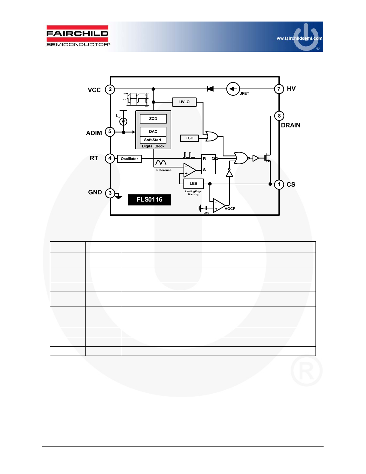
1.3. Internal Block Diagram
Figure 1. Internal Block Diagram
Pin No. Symbol Description
1 CS
2 VCC
3 GND
4 RT
5 ADIM
6 NC No Connection.
7 HV
8 DRAIN
Current Sense. Limits output current, depending on the sensing resistor
voltage. The CS pin is also used to set the LED current regulation.
VCC. Supply pin for stable IC operation ZCD signal detection used for accurate
PFC function.
GROUND. Ground for the IC.
RT. Programmable operating frequency using an external resistor. The IC has a
fixed frequency when this pin is open or floating.
Analog Dimming. Connects to the internal current source and can change the
output current using an external resistor. If ADIM is not used, connect a 0.1µF
bypass capacitor between ADIM and GND.
High Voltage. Connects to the high-voltage line and supplies current to the IC.
High Voltage. Internal switching FET drain pin.
© 2012 Fairchild Semiconductor Corporation 4 FEB-L032_FLS0116 • Rev. 1.0.1
Page 5
2. General Specifications for Evaluation Board
All data for this table was measured at an ambient temperature of 25°C.
Table 1. Summary of Features and Performance
Description Symbol Value Comments
V
90V Minimum Input Voltage
IN.MIN
Input Voltage Range
AC Input Frequency
Output Voltage
Output Current
Output Power
(1)
(2)
Output Power 2.7W
Efficiency >78% At Full Load
Temperature
PCB Size
Initial Application LED Bulb
Notes:
1. The output current has I
in parallel with the LED. Ensure the capacitor voltage rating is high enough to withstand an
open-LED condition or use a Zener diode for protection.
2. The output power is not equal to the apparent power due to the slight phase shift between the
output voltage and current.
V
IN.NORMAL
V
Freq
Freq
V
OUT,MAX
V
OUT,NORMAL
V
I
OUT.NORMAL
CC Deviation < ±1.3%
T
T
T
FRD,UF4007
T
CS resistor
T
110V / 220V Normal Input Voltage
265V Maximum Input Voltage
IN.MAX
47Hz Minimum Input Frequency
IN.MIN
64Hz Maximum Input Frequency
IN.MAX
30V Maximum Output Voltage
28V Normal Output Voltage
26V Minimum Output Voltage
OUT,MIN
97mA Normal Output Current
Line Input Voltage Change:
90~265VAC
< 73°C
FLS0116
< 44°C
DM filter
< 47°C
At Full Load (all at open-frame, room
temperature / still air)
< 59°C
< 66°C
inductor
20mm (width) x 30mm (length )x
18mm (height)
ripple. To reduce ripple current, use a large electrolytic capacitor
LEDPK
© 2012 Fairchild Semiconductor Corporation 5 FEB-L032_FLS0116 • Rev. 1.0.1
Page 6
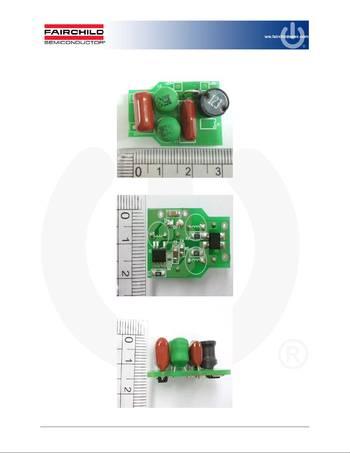
2.1. Photographs of Evaluation Board
Figure 2. Top View (20mm x 30mm)
Figure 3. Bottom View (20mm x 30mm)
Figure 4. Side View (18mm)
© 2012 Fairchild Semiconductor Corporation 6 FEB-L032_FLS0116 • Rev. 1.0.1
Page 7
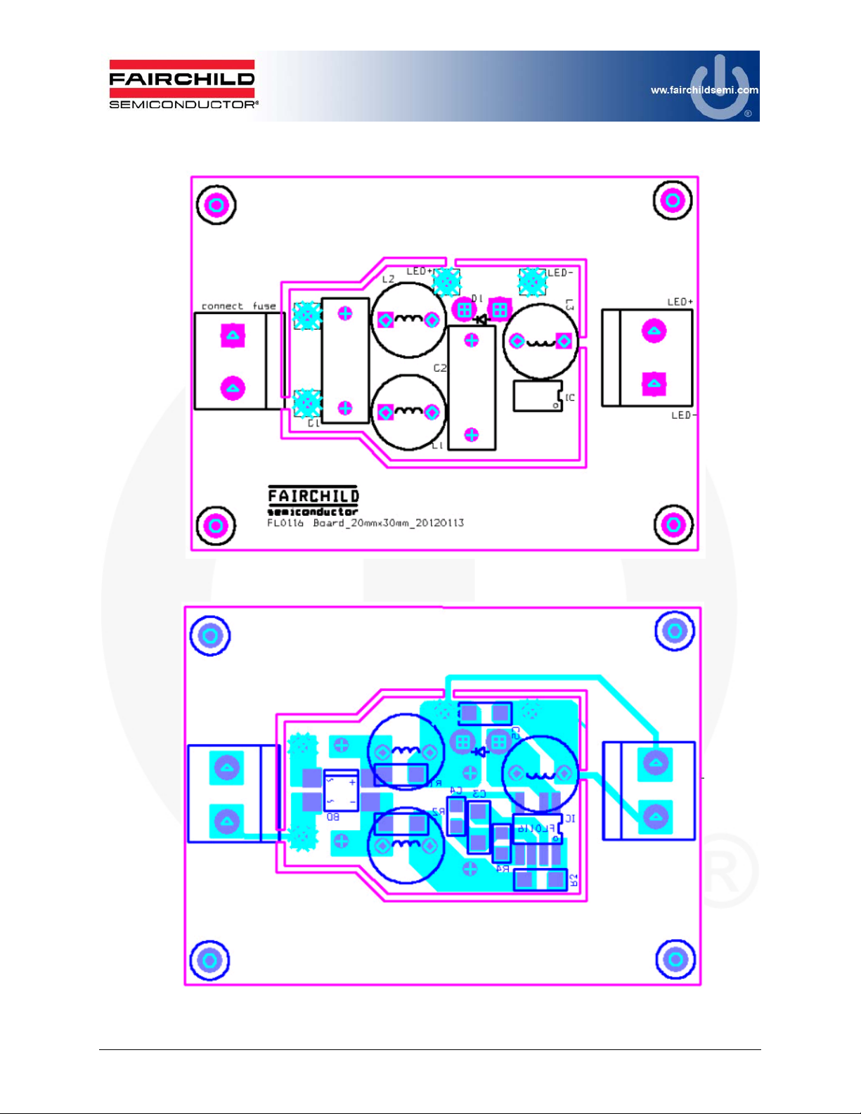
2.2. Printed Circuit Board
Figure 5. Top Side
Figure 6. Bottom Side
© 2012 Fairchild Semiconductor Corporation 7 FEB-L032_FLS0116 • Rev. 1.0.1
Page 8
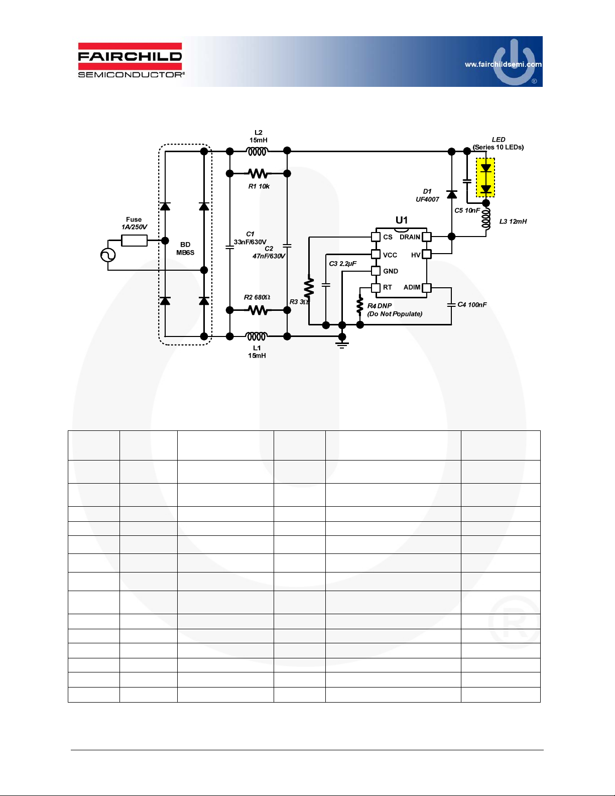
2.3. Schematic
Figure 7. Evaluation Board Schematic
2.4. Bill Of Materials
Item No.
1 U1 FLS0116M 1 Controller
2 BD MB6S 1 0.5A/600V, Bridge Diode
3 C1 MPE 630V333K 1 333/630VAC, Film Capacitor Sungho
4 C2 MPE 630V473K 1 473/630VAC, Film Capacitor Sungho
5 C3 C1206C225K3PACTU 1
6 C4
7 C5 C1206C103KDRACTU 1
8 D1 UF4007 1 1A/1000V, Ultra-Fast Recovery
9 L1,L2 R06153KT00 2 15mH, Filter Inductor Bosung
10 L3 RFB0810-123L 1 12mH, Inductor Coil Craft
11 R1 RC1206JR-07103RL 1 10kΩ, SMD Resistor 3216 Yageo
12 R2 RC1206JR-07680RL 1 680Ω, SMD Resistor 3216 Yageo
13 R3 RC1206JR-073RL 1 3Ω, SMD Resistor 3216 Yageo
- R4 - 0 Open
Part
Reference
Part Number Qty. Description Manufacturer
Fairchild
Semiconductor
Fairchild
Semiconductor
Kemet
Kemet
Kemet
Fairchild
Semiconductor
C0805C104K3RACTU
225/25V SMD Capacitor 3216
1
104/25V SMD Capacitor 2012
103/630V SMD Capacitor 3216
© 2012 Fairchild Semiconductor Corporation 8 FEB-L032_FLS0116 • Rev. 1.0.1
Page 9

3. Performance of Evaluation Board
Table 2. Test Condition & Equipments
Test Temperature
Test Equipment
AC Source : PCR500L by Kikusui
Power Meter : PZ4000 by Yokogawa
Oscilloscope : Waverunner 64Xi by LeCroy
EMI Test Receiver: ESCS30 by ROHDE & SCHWARZ
Two-Line V-Network: ENV216 by ROHDE & SCHWARZ
Thermometer : CAM SC640 by FLIR SYSTEMS
LED: EHP-AX08EL/GT01H-P03 (3W) by Everlight
TA = 25°C
© 2012 Fairchild Semiconductor Corporation 9 FEB-L032_FLS0116 • Rev. 1.0.1
Page 10
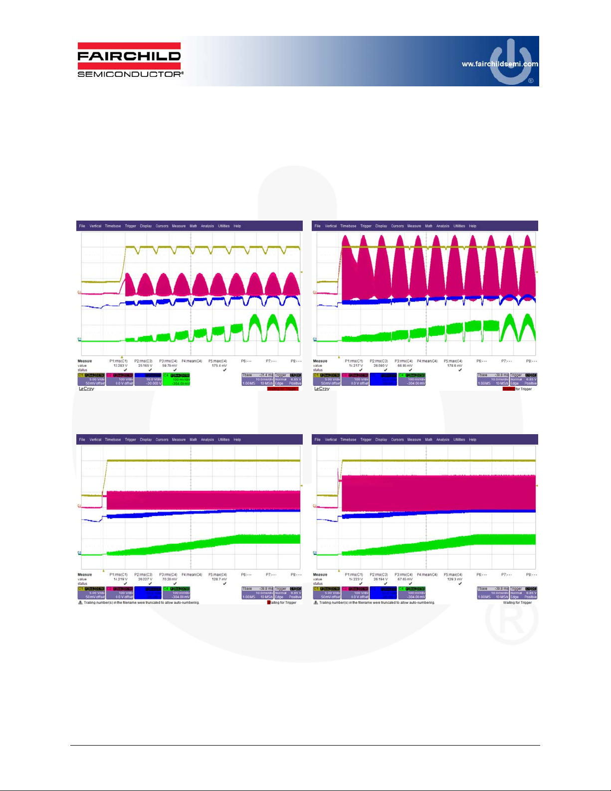
3.1. Typical Waveforms: Startup
V
V
V
V
Figure 8 through Figure 11 show the typical startup performance at different input
voltage conditions. When AC input voltage is applied to the system, the FLS0116
automatically operates in AC Mode after finishing an internally fixed, seven-cycle, softstart period. Figure 10 and Figure 11 show the soft-start characteristics when a DC input
voltage is applied.
CH1: VCC, CH2:
DRAIN
, CH3: V
LED
, CH4: I
Figure 8. Soft-Start, AC Mode, 90V
CH1: VCC, CH2:
DRAIN
, CH3: V
LED
, CH4: I
Figure 10. Soft-Start, DC Mode, 100V
AC
DC
LED
LED
CH1: V
, CH2:
CC
DRAIN
, CH3: V
LED
, CH4: I
LED
Figure 9. Soft-Start, AC Mode, 265VAC
CH1: V
, CH2:
CC
DRAIN
, CH3: V
LED
, CH4: I
LED
Figure 11. Soft-Start, DC Mode, 200VDC
© 2012 Fairchild Semiconductor Corporation 10 FEB-L032_FLS0116 • Rev. 1.0.1
Page 11
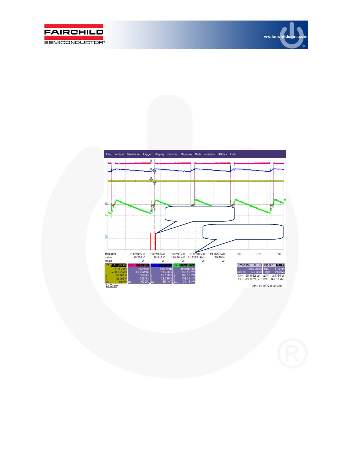
3.2. Operating Frequency & Minimum Duty
The programmable switching frequency is between 20kHz ~ 250kHz, determined by
selecting the RT resistor value. If no RT resistor is used (RT pin OPEN), the FLS0116
default switching frequency is set to 45kHz. The maximum duty ratio is fixed below 50%
and has a fixed minimum typical on-time of 400ns. There are two crucial points to design
properly. The first is consideration of the minimum duty ratio at minimum input voltage
because the FLS0116 is limited to 50% duty ratio. The second consideration is minimum
on-time at maximum input voltage condition. The FLS0116 cannot control output power
when the operating conditions are such that the required on-time is less than the 400ns
minimum on-time.
Minimum On Time: 2.13µs
Switching Frequency: 44.52kHz
CH1: V
Figure 12. Operating Frequency & Minimum Duty Ratio
, CH2: V
CC
DRAIN
, CH3: V
LED
, CH4: I
LED
© 2012 Fairchild Semiconductor Corporation 11 FEB-L032_FLS0116 • Rev. 1.0.1
Page 12
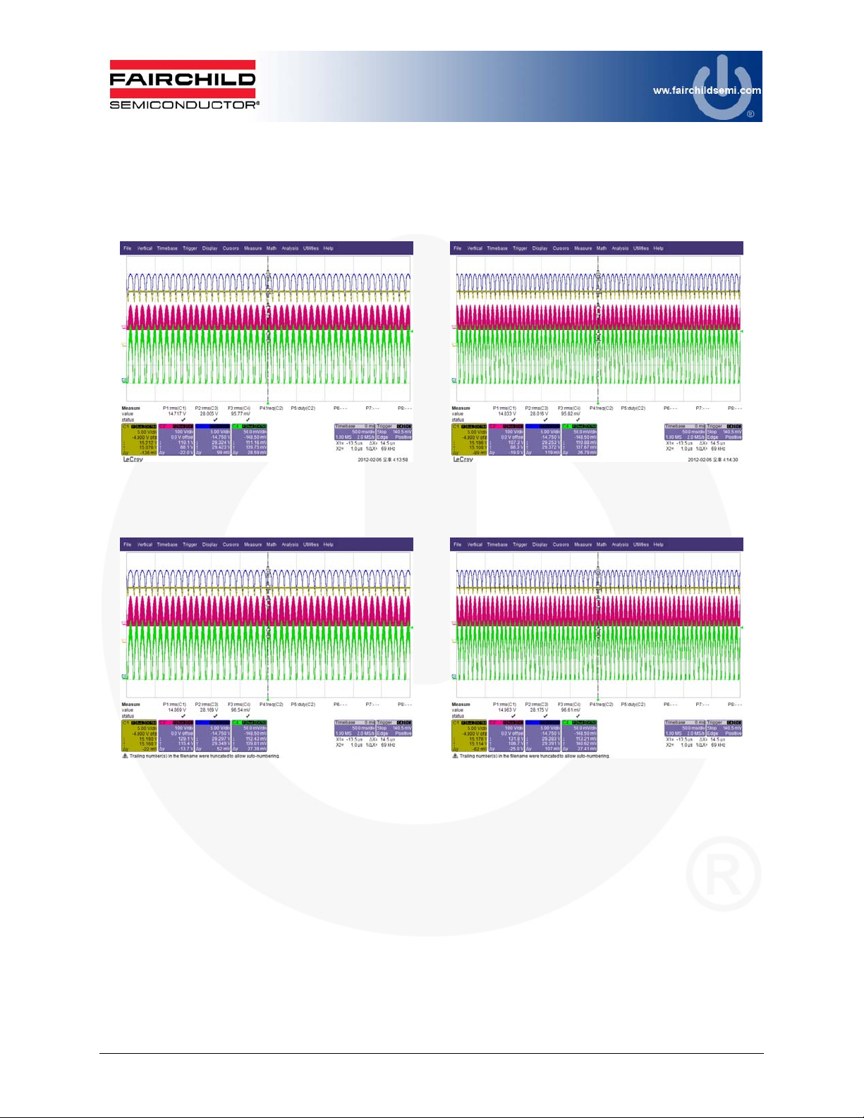
3.3. Typical Waveforms: Steady State
V
Figure 13 through Figure 22 show the normal operation waveform by input voltage and
input frequency. The output voltage and current maintains a certain output level with
120Hz ripple, as shown in the test results in Table 2.
CH1: VCC, CH2: V
Figure 13. Input Voltage: 90V
DRAIN
, CH3: V
, CH4: I
LED
, Input Frequency: 47Hz
AC
LED
CH1: VCC, CH2:
Figure 14. Input Voltage: 90VAC, Input Frequency:
DRAIN
, CH3: V
64Hz
LED
, CH4: I
LED
H1: VCC, CH2: V
Figure 15. Input Voltage: 110V
DRAIN
47Hz
, CH3: V
AC
LED
, CH4: I
LED
, Input Frequency:
H1: V
, CH2: V
CC
DRAIN
, CH3: V
Figure 16. Input Voltage: 110V
64Hz
, CH4: I
LED
, Input Frequency:
AC
LED
© 2012 Fairchild Semiconductor Corporation 12 FEB-L032_FLS0116 • Rev. 1.0.1
Page 13
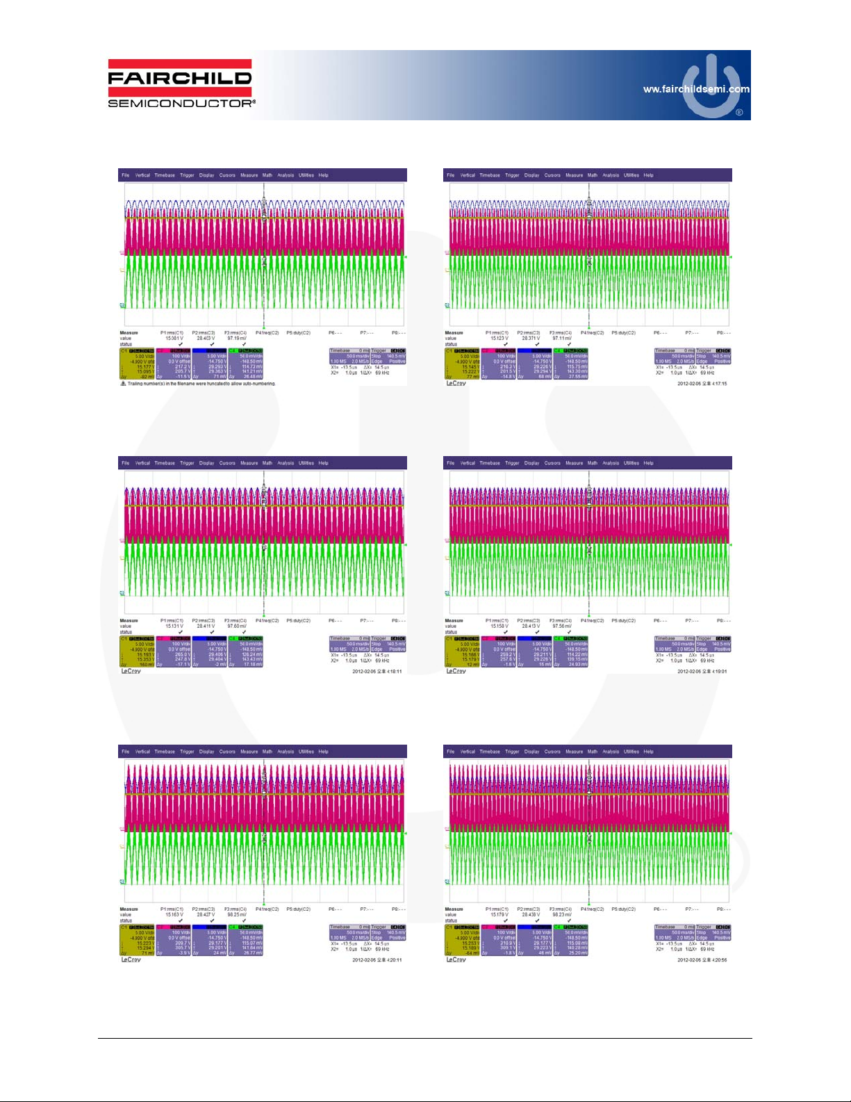
3.4. Typical Operating Waveforms: Output Characteristics
V
V
V
V
V
CH1: VCC, CH2:
Figure 17. Input Voltage: 180V
DRAIN
47Hz
, CH3:
LED
, Input Frequency:
AC
, CH4: I
LED
CH1: V
, CH2:
CC
DRAIN
, CH3: V
Figure 18. Input Voltage: 180V
64Hz
, CH4: I
LED
, Input Frequency:
AC
LED
CH1: VCC, CH2:
Figure 19. Input Voltage: 220VAC, Input Frequency:
H1: VCC, CH2: V
Figure 21. Input Voltage: 265V
© 2012 Fairchild Semiconductor Corporation 13 FEB-L032_FLS0116 • Rev. 1.0.1
DRAIN
47Hz
DRAIN
47Hz
, CH3: V
, CH3: V
AC
, CH4: I
LED
LED
, CH4: I
LED
LED
, Input Frequency:
CH1: V
, CH2:
CC
DRAIN
, CH3: V
LED
, CH4: I
LED
Figure 20. Input Voltage: 220VAC, Input Frequency:
64Hz
H1: V
, CH2: V
CC
Figure 22. Input Voltage: 265V
DRAIN
, CH3: V
AC
LED
, CH4: I
LED
, Input Frequency:
64Hz
Page 14

Table 3. Output Characteristics by Input Voltage and Frequency
90VAC
110VAC
180VAC
220VAC
265VAC
47Hz 64Hz
V
LED(RMS)
28.01V 95.77mA 28.02V 95.82mA
28.17V 96.54mA 28.17V 96.61mA
28.40V 97.19mA 28.37V 97.11mA
28.41V 97.60mA 28.41V 97.56mA
28.43V 98.25mA 28.43V 98.23mA
I
LED(RMS)
V
LED(RMS)
I
LED(RMS)
© 2012 Fairchild Semiconductor Corporation 14 FEB-L032_FLS0116 • Rev. 1.0.1
Page 15
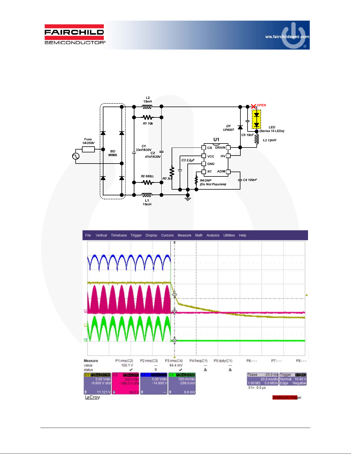
3.5. Typical Waveforms: Abnormal Mode (LED Open)
Figure 23 and Figure 24 show the open-load condition test method and result. When the
LED disconnects from the system, the IC cannot operate because the HV pin is
disconnected.
Figure 23. Open-Load Condition Test
CH1: VCC, CH2: V
Figure 24. Test Results of Open-Load Condition
© 2012 Fairchild Semiconductor Corporation 15 FEB-L032_FLS0116 • Rev. 1.0.1
DRAIN
, CH3: V
, CH4: I
LED
LED
Page 16
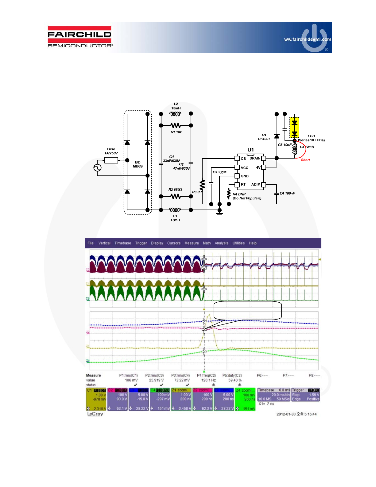
3.6. Typical Waveforms: Abnormal Mode (Inductor Short)
Figure 25 and Figure 26 show the test method and result of an inductor short. The
FLS0116 uses an abnormal over-current protection (AOCP) function, limiting the current
on RCS in the event of an inductor short.
Figure 25. Inductor-Short Condition
When CS pin voltage reaches
2.5V, AOCP is enabled after
70ns internal delay time
CH1: VCS, CH2: V
Figure 26. Test Results of Inductor Short Condition
© 2012 Fairchild Semiconductor Corporation 16 FEB-L032_FLS0116 • Rev. 1.0.1
DRAIN
, CH3: V
, CH4: I
LED
LED
Page 17
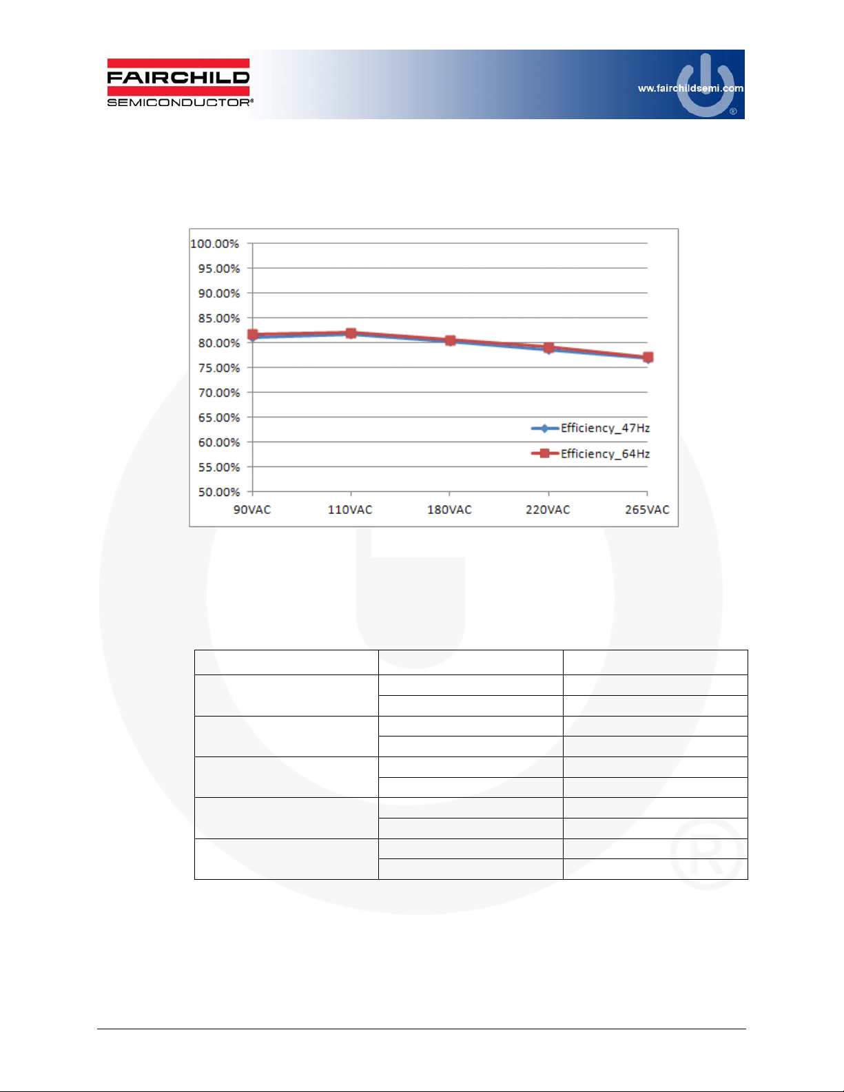
3.7. System Efficiency
Figure 27 shows system efficiency results for different AC input voltage frequency
conditions. As shown, the input frequency has negligible effect on system efficiency.
Efficiency
Input Voltage
Figure 27. System Efficiency
Table 4. Efficiency Test Results
Input Voltage (V
90VAC
110VAC
180VAC
220VAC
265VAC
) Frequency (Hz) Efficiency (%)
AC
47Hz 81.12
64Hz 81.73
47Hz 81.72
64Hz 82.08
47Hz 80.26
64Hz 82.57
47Hz 78.64
64Hz 79.12
47Hz 76.84
64Hz 77.14
© 2012 Fairchild Semiconductor Corporation 17 FEB-L032_FLS0116 • Rev. 1.0.1
Page 18
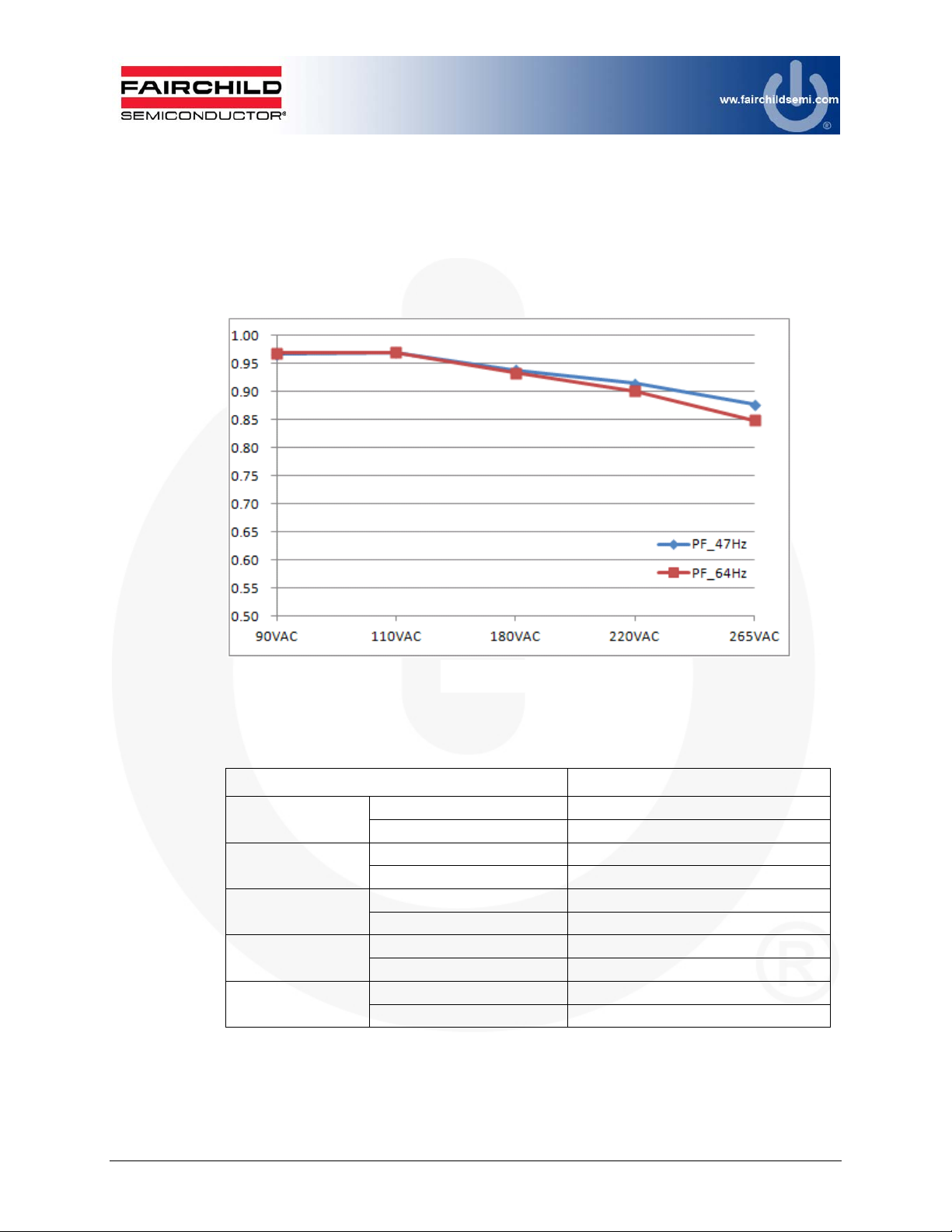
3.8. Power Factor at Rated Load Condition
Figure 28 shows the system Power Factor (PF) performance for the entire input voltage
range (90V
changes slightly according to the input frequency, but can achieve over 0.85 at 265V
condition.
PF
to 265VAC) at different input frequency conditions (47Hz, 64Hz). The PF
AC
AC
Figure 28. Power Factor
Input Voltage
Table 5. PF Test Results
Input Voltage Power Factor
90VAC
110VAC
180VAC
220VAC
265VAC
47Hz 0.97
64Hz 0.97
47Hz 0.97
64Hz 0.97
47Hz 0.94
64Hz 0.94
47Hz 0.91
64Hz 0.90
47Hz 0.88
64Hz 0.85
© 2012 Fairchild Semiconductor Corporation 18 FEB-L032_FLS0116 • Rev. 1.0.1
Page 19
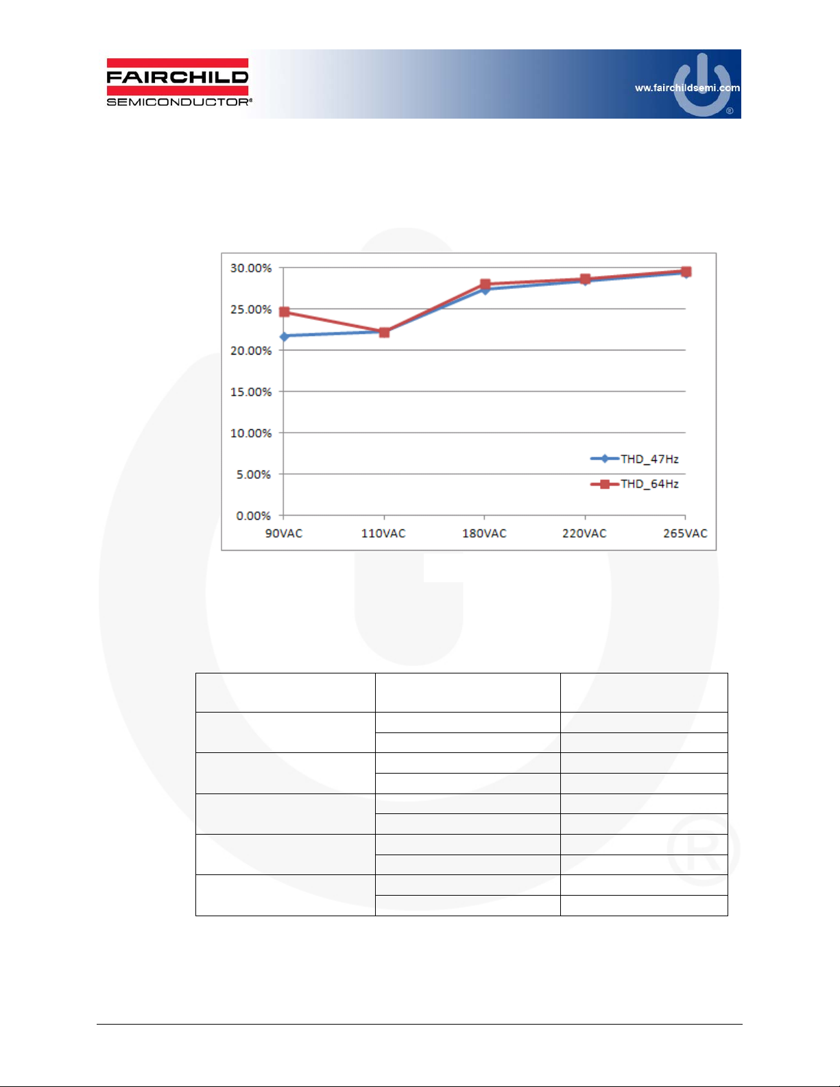
3.9. Total Harmonic Distortion
Figure 29 shows the Total Harmonic Distortion (THD) performance at different input
frequencies. Test results are quite similar, except the 90V
international regulations (under 30%).
THD
condition, but meet
AC
Input Voltage
Figure 29. THD Performance
Table 6. THD Test Results
Input Voltage (V
90VAC
110VAC
180VAC
220VAC
265VAC
) Frequency (Hz) THD (%)
AC
47Hz 21.74
64Hz 24.70
47Hz 22.24
64Hz 22.23
47Hz 27.38
64Hz 28.09
47Hz 28.46
64Hz 28.72
47Hz 29.37
64Hz 29.64
© 2012 Fairchild Semiconductor Corporation 19 FEB-L032_FLS0116 • Rev. 1.0.1
Page 20
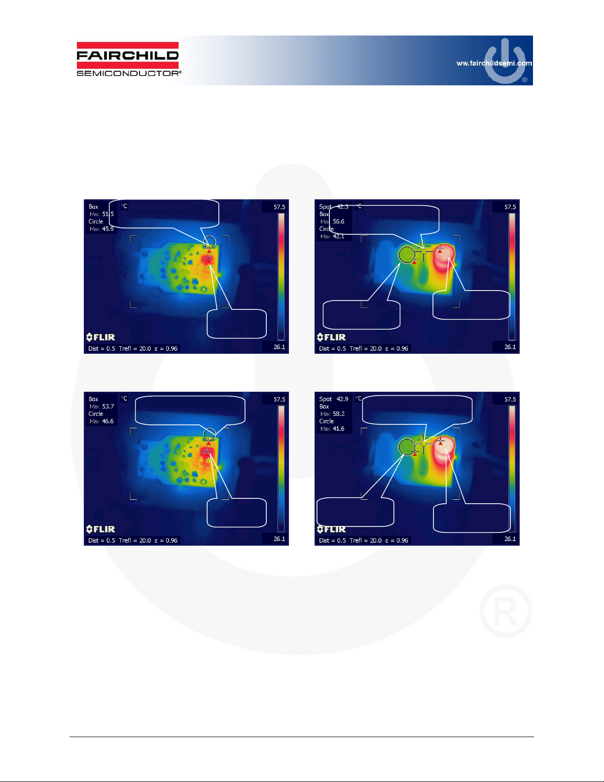
3.10. Thermal Performance
V
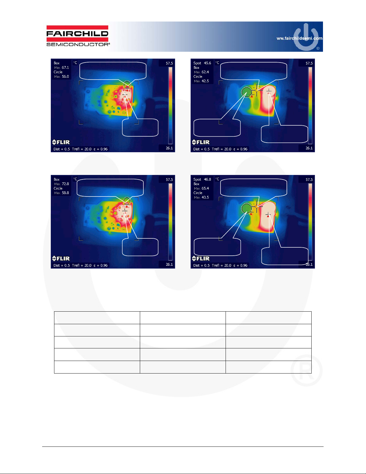
Figure 30 through Figure 37 show the steady-state thermal test results with different input
voltage conditions. Inductor L3 has the highest temperature on the top side of the PCB
due to copper resistance. The FLS0116 has the highest temperature on the bottom side of
the PCB due to power loss associated with the high-voltage device. The IC temperature is
67.1°C for the 220V
input condition.
AC
CS Resistor (R3) TEMP
: 45.9℃
IC TEMP
: 51.5℃
Figure 30. Bottom-Side Temperature at 90V
Condition (IC)
CS Resistor (R3) TEMP
: 46.6℃
Diode (D1) TEMP
: 42.3℃
Inductor TEMP
Filter L2 TEMP
: 42.1℃
: 56.6℃
AC
Figure 31. Top-Side Temperature at 90V
(Inductor)
Diode (D1) TEMP
: 42.9℃
AC
Condition
IC TEMP
: 53.7℃
Filter L2 TEMP
: 41.6℃
Inductor TEMP
: 58.2℃
Figure 32. Bottom-Side Temperature at 110
AC
Condition (IC)
© 2012 Fairchild Semiconductor Corporation 20 FEB-L032_FLS0116 • Rev. 1.0.1
Figure 33. Top-Side Temperature at 110V
(Inductor)
Condition
AC
Page 21
V
V
V
CS Resistor(R3) TEMP
: 56.0℃
IC TEMP
: 67.1℃
Figure 34. Bottom-Side Temperature at 220
Condition (IC)
CS Resistor(R3) TEMP
: 58.8℃
Diode (D1) TEMP
: 45.6℃
Filter L2 TEMP
: 42.5℃
Inductor TEMP
: 62.4℃
AC
Figure 35. Top-Side Temperature at 220V
(Inductor)
Diode (D1) TEMP
: 46.8℃
AC
Condition
IC TEMP
: 72.8℃
Figure 36. Bottom-Side Temperature at 264
Condition (IC)
Table 7. Temperature Performance by Input Voltage
Input Voltage (V
90VAC 51.5°C 56.6°C
110VAC 53.7°C 58.2°C
220VAC 67.1°C 62.4°C
265VAC 72.8°C 65.4°C
) TIC T
AC
Filter L2 TEMP
: 43.5℃
Inductor TEMP
: 65.4℃
AC
Figure 37. Top-Side Temperature at 264
(Inductor)
INDUCTOR
AC
Condition
© 2012 Fairchild Semiconductor Corporation 21 FEB-L032_FLS0116 • Rev. 1.0.1
Page 22
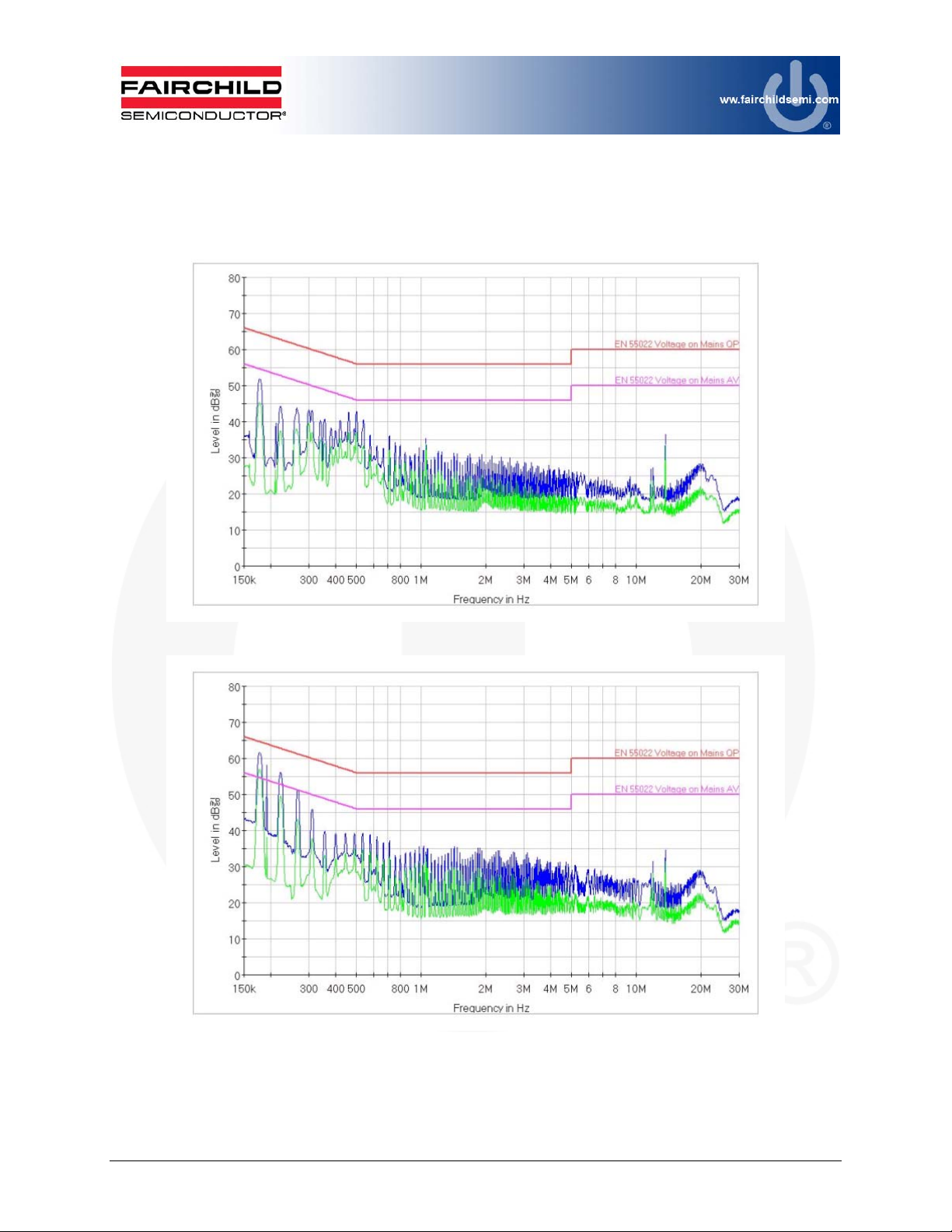
3.11. EMI Test Results
EMI test measurements were conducted in observance of CISPR22 criteria, which has
stricter limits than CISPR15 for lighting applications.
Figure 38. Conducted Emission-Line at 110VAC Input Condition, Full Load (10-LED Series)
Figure 39. Conducted Emission-Line at 220VAC Input Condition, Full Load (10-LED Series)
© 2012 Fairchild Semiconductor Corporation 22 FEB-L032_FLS0116 • Rev. 1.0.1
Page 23
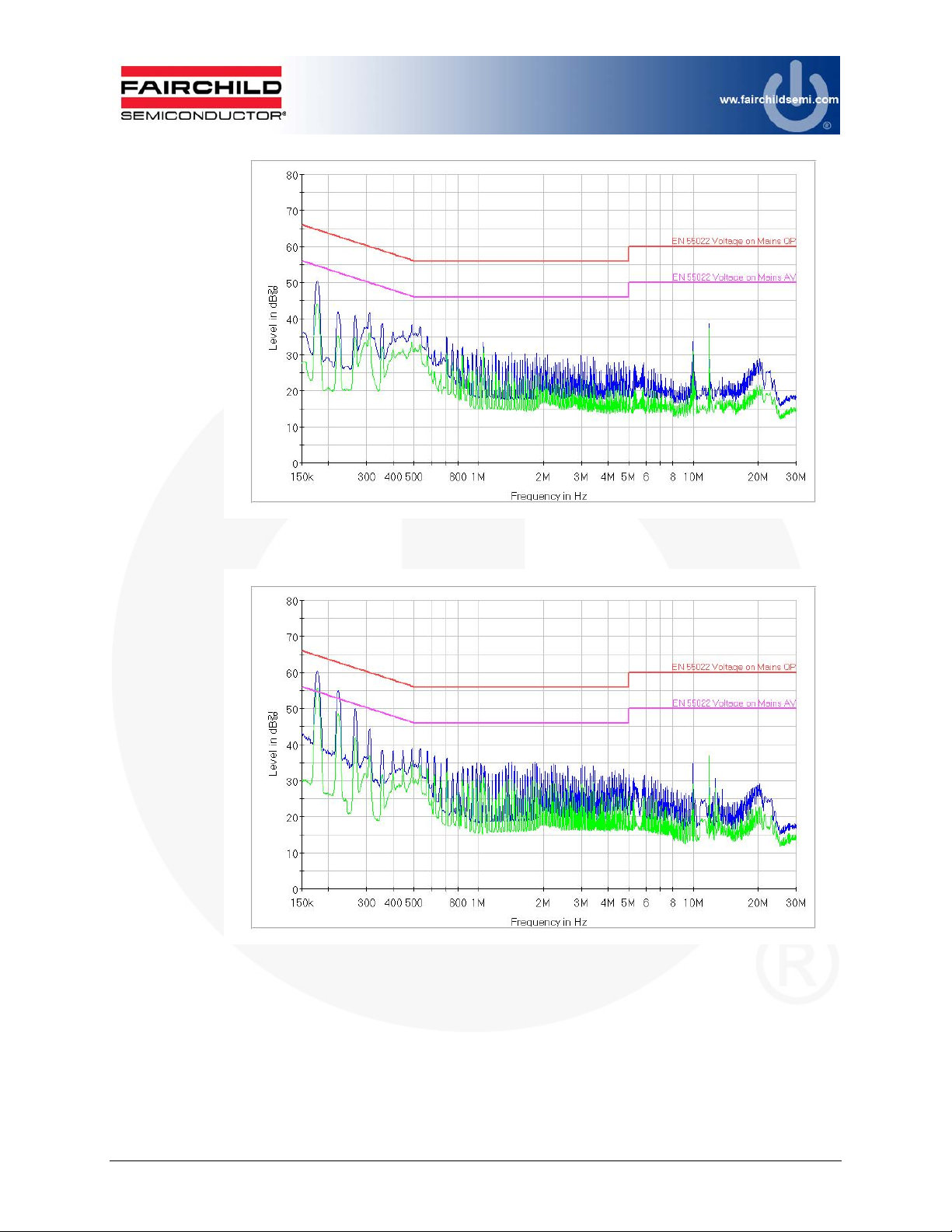
Figure 40. Conducted Emission-Line at 110VAC Input Condition, Full Load
(10-LED Series)
Figure 41. Conducted Emission-Neutral at 220VAC Input Condition, Full Load
(10-LED Series)
© 2012 Fairchild Semiconductor Corporation 23 FEB-L032_FLS0116 • Rev. 1.0.1
Page 24

4. Revision History
Rev. Date Description
1.0.0 May 2012
1.0.1 June 2012
WARNING AND DISCLAIMER
Replace components on the Evaluation Board only with those parts shown on the parts list (or Bill of Materials) in the Users’ Guide. Contact an
authorized Fairchild representative with any questions.
This board is intended to be used by certified professionals, in a lab environment, following proper safety procedures. Use at your own risk. The
Evaluation board (or kit) is for demonstration purposes only and neither the Board nor this User’s Guide constitute a sales contract or create any kind
of warranty, whether express or implied, as to the applications or products involved. Fairchild warrantees that its products meet Fairchild’s published
specifications, but does not guarantee that its products work in any specific application. Fairchild reserves the right to make changes without notice to
any products described herein to improve reliability, function, or design. Either the applicable sales contract signed by Fairchild and Buyer or, if no
contract exists, Fairchild’s standard Terms and Conditions on the back of Fairchild invoices, govern the terms of sale of the products described herein.
DISCLAIMER
FAIRCHILD SEMICONDUCTOR RESERVES THE RIGHT TO MAKE CHANGES WITHOUT FURTHER NOTICE TO ANY PRODUCTS HEREIN TO
IMPROVE RELIABILITY, FUNCTION, OR DESIGN. FAIRCHILD DOES NOT ASSUME ANY LIABILITY ARISING OUT OF THE APPLICATION OR
USE OF ANY PRODUCT OR CIRCUIT DESCRIBED HEREIN; NEITHER DOES IT CONVEY ANY LICENSE UNDER ITS PATENT RIGHTS, NOR
THE RIGHTS OF OTHERS.
LIFE SUPPORT POLICY
FAIRCHILD’S PRODUCTS ARE NOT AUTHORIZED FOR USE AS CRITICAL COMPONENTS IN LIFE SUPPORT DEVICES OR SYSTEMS
WITHOUT THE EXPRESS WRITTEN APPROVAL OF THE PRESIDENT OF FAIRCHILD SEMICONDUCTOR CORPORATION.
As used herein:
1. Life support devices or systems are devices or systems which, (a)
are intended for surgical implant into the body, or (b) support or
sustain life, or (c) whose failure to perform when properly used in
accordance with instructions for use provided in the labeling, can be
reasonably expected to result in significant injury to the user.
ANTI-COUNTERFEITING POLICY
Fairchild Semiconductor Corporation's Anti-Counterfeiting Policy. Fairchild's Anti-Counterfeiting Policy is also stated on our external website,
www.fairchildsemi.com, under Sales Support.
Counterfeiting of semiconductor parts is a growing problem in the industry. All manufacturers of semiconductor products are experiencing
counterfeiting of their parts. Customers who inadvertently purchase counterfeit parts experience many problems such as loss of brand reputation,
substandard performance, failed applications, and increased cost of production and manufacturing delays. Fairchild is taking strong measures to
protect ourselves and our customers from the proliferation of counterfeit parts. Fairchild strongly encourages customers to purchase Fairchild parts
either directly from Fairchild or from Authorized Fairchild Distributors who are listed by country on our web page cited above. Products customers buy
either from Fairchild directly or from Authorized Fairchild Distributors are genuine parts, have full traceability, meet Fairchild's quality standards for
handling and storage and provide access to Fairchild's full range of up-to-date technical and product information. Fairchild and our Authorized
Distributors will stand behind all warranties and will appropriately address any warranty issues that may arise. Fairchild will not provide any warranty
coverage or other assistance for parts bought from Unauthorized Sources. Fairchild is committed to combat this global problem and encourage our
customers to do their part in stopping this practice by buying direct or from authorized distributors.
EXPORT COMPLIANCE STATEMENT
These commodities, technology, or software were exported from the United States in accordance with the Export Administration Regulations for the
ultimate destination listed on the commercial invoice. Diversion contrary to U.S. law is prohibited.
U.S. origin products and products made with U.S. origin technology are subject to U.S Re-export laws. In the event of re-export, the user will be
responsible to ensure the appropriate U.S. export regulations are followed.
First Release
Changing Power Rating
Changing Form
2. A critical component is any component of a life support device or
system whose failure to perform can be reasonably expected to
cause the failure of the life support device or system, or to affect its
safety or effectiveness.
© 2012 Fairchild Semiconductor Corporation 24 FEB-L032_FLS0116 • Rev. 1.0.1
 Loading...