

Page 1
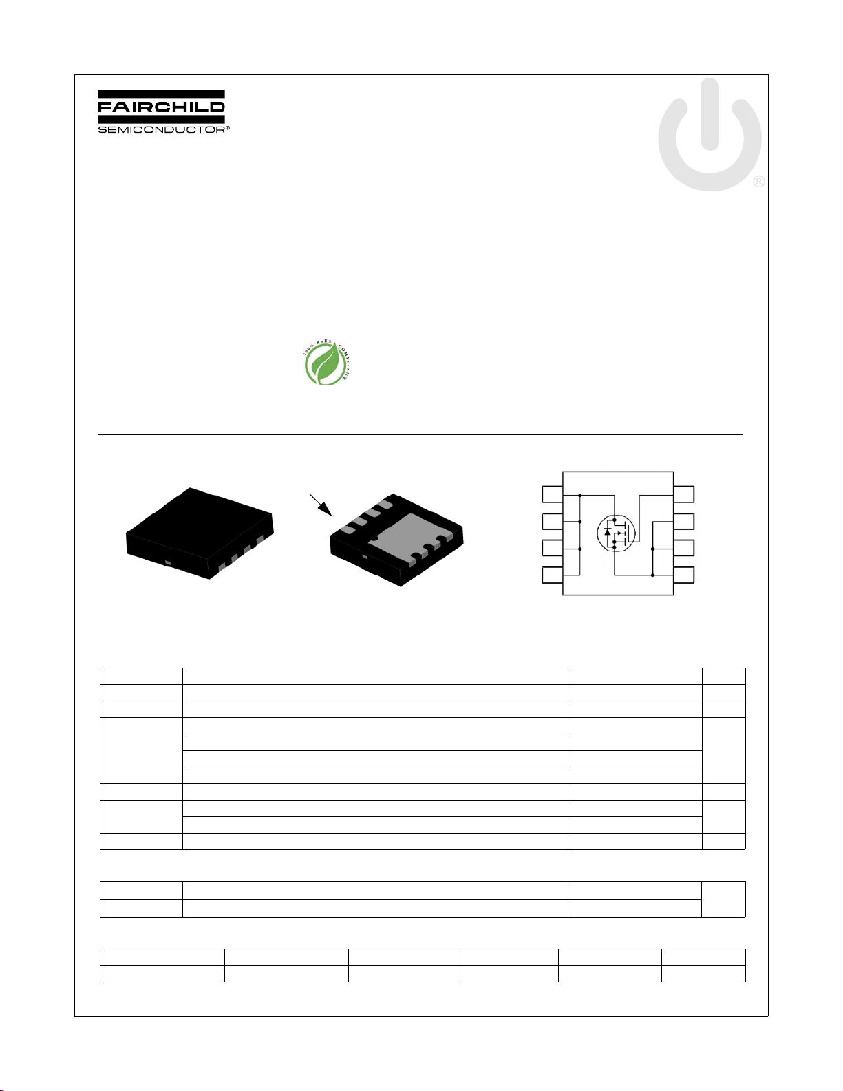
FDMC86102L
G
S
S
S
D
D
D
D
5
6
7
8
3
2
1
4
Bottom
D
D
D
D
S
S
S
G
Top
Pin 1
MLP 3.3x3.3
N-Channel Power Trench® MOSFET
100 V, 18 A, 23 mΩ
Features
Max r
Max r
Low Profile - 1 mm max in Power 33
RoHS Compliant
= 23 mΩ at VGS = 10 V, ID = 7 A
DS(on)
= 34 mΩ at VGS = 4.5 V, ID = 5.5 A
DS(on)
General Description
This N-Channel MOSFET is produced using Fairchild
Semiconductor‘s advanced Power Trench
been especially tailored to minimize the on-state resistance and
yet maintain superior switching performance.
Application
DC - DC Conversion
December 2010
®
process that has
FDMC86102L N-Channel PowerTrench
®
MOSFET
MOSFET Maximum Ratings T
Symbol Parameter Ratings Units
V
DS
V
GS
I
D
E
AS
P
D
, T
T
J
STG
Thermal Characteristics
R
θJC
R
θJA
Package Marking and Ordering Information
Device Marking Device Package Reel Size Tape Width Quantity
FDMC86102L FDMC86102L Power 33 13 ’’ 12 mm 3000 units
©2010 Fairchild Semiconductor Corporation
FDMC86102L Rev.C
Drain to Source Voltage 100 V
Gate to Source Voltage ±20 V
Drain Current -Continuous (Package limited) TC = 25 °C 18
-Continuous (Silicon limited) T
-Continuous T
-Pulsed 30
Single Pulse Avalanche Energy (Note 3) 63 mJ
Power Dissipation TC = 25 °C 41
Power Dissipation T
Operating and Storage Junction Temperature Range -55 to +150 °C
Thermal Resistance, Junction to Case 3
Thermal Resistance, Junction to Ambient (Note 1a) 53
= 25 °C unless otherwise noted
A
= 25 °C 30
C
= 25 °C (Note 1a) 7
A
= 25 °C (Note 1a) 2.3
A
1
A
W
°C/W
www.fairchildsemi.com
Page 2
FDMC86102L N-Channel PowerTrench
Electrical Characteristics T
= 25 °C unless otherwise noted
J
Symbol Parameter Test Conditions Min Typ Max Units
Off Characteristics
BV
ΔBV
ΔT
I
DSS
I
GSS
DSS
DSS
J
Drain to Source Breakdown Voltage ID = 250 μA, VGS = 0 V 100 V
Breakdown Voltage Temperature
Coefficient
Zero Gate Voltage Drain Current VDS = 80 V, V
Gate to Source Leakage Current VGS = ±20 V, V
I
= 250 μA, referenced to 25 °C 71 mV/°C
D
= 0 V 1 μA
GS
= 0 V ±100 nA
DS
On Characteristics
V
GS(th)
ΔV
ΔT
r
DS(on)
g
FS
GS(th)
J
Gate to Source Threshold Voltage VGS = VDS, ID = 250 μA11.83V
Gate to Source Threshold Voltage
Temperature Coefficient
Static Drain to Source On Resistance
I
= 250 μA, referenced to 25 °C -6 mV/°C
D
V
= 10 V, ID = 7 A 18.9 23
GS
= 4.5 V, ID = 5.5 A 24.9 34
GS
= 10 V, ID = 7 A, TJ = 125 °C 31.9 39
V
GS
Forward Transconductance VDS = 5 V, ID = 7 A 26 S
Dynamic Characteristics
C
iss
C
oss
C
rss
R
g
Input Capacitance
Output Capacitance 178 240 pF
Reverse Transfer Capacitance 7.6 15 pF
Gate Resistance 0.5 Ω
Switching Characteristics
t
d(on)
t
r
t
d(off)
t
f
Q
g(TOT)
Q
g(TOT)
Q
gs
Q
gd
Turn-On Delay Time
Rise Time 2.2 10 ns
Turn-Off Delay Time 19 34 ns
Fall Time 2.4 10 ns
Total Gate Charge V
Total Gate Charge V
Total Gate Charge 2.7 nC
Gate to Drain “Miller” Charge 2.3 nC
= 50 V, VGS = 0 V,
V
DS
f = 1 MHz
= 50 V, ID = 7 A,
V
DD
V
= 10 V, R
GS
= 0 V to 10 V
GS
= 0 V to 4.5 V 7.3 11 nC
GS
GEN
= 6 Ω
V
DD
I
D
= 50 V,
= 7 A
999 1330 pF
7.7 16 ns
15 22 nC
mΩV
®
MOSFET
Drain-Source Diode Characteristics
V
SD
t
rr
Q
rr
NOTES:
is determined with the devi ce m ount ed on a 1 in2 pad 2 oz copper pad on a 1.5 x 1.5 in. board of FR-4 material. R
1. R
θJA
the user's board design.
2. Pulse Test: Pulse Width < 300 μs, Duty cycle < 2.0%.
3. Starting TJ = 25 °C; N-ch: L = 1 mH, IAS = 11.3 A, VDD = 90 V, VGS = 10 V.
©2010 Fairchild Semiconductor Corporation
FDMC86102L Rev.C
Source to Drain Diode Forward Voltage
Reverse Recovery Time
Reverse Recovery Charge 45 72 nC
a) 53 °C/W when mounted on
a 1 in
V
GS
V
GS
= 7 A, di/dt = 100 A/μs
I
F
2
pa d of 2 oz co pper
= 0 V, IS = 7 A (Note 2) 0.81 1.3
= 0 V, IS = 2 A (Note 2) 0.74 1.2
45 72 ns
is guaranteed by design while R
θJC
b) 125 °C/W when mounted on a
minimum pad of 2 oz copper
2
θCA
www.fairchildsemi.com
V
is determined by
Page 3
FDMC86102L N-Channel PowerTrench
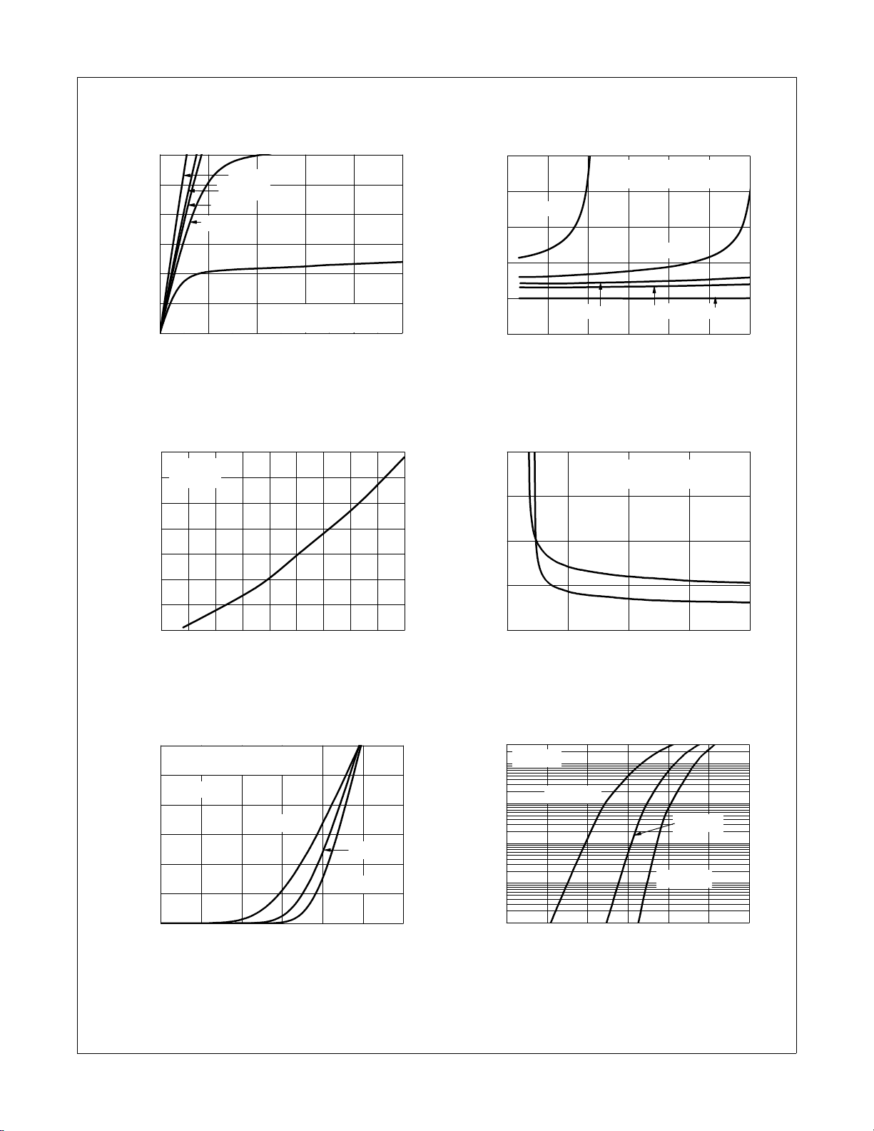
012345
0
5
10
15
20
25
30
PULSE DURA TION = 80 μs
DUTY CYCLE = 0.5% MAX
VGS = 3.5 V
VGS = 4.5 V
VGS = 10 V
VGS = 4 V
VGS = 3 V
I
D
, DRAIN CURRENT (A)
V
DS
, DRAIN TO SOURCE VOLTAGE (V)
0 5 10 15 20 25 30
0
1
2
3
4
5
VGS = 3.5 V
PULSE DURATION = 80 μs
DUTY CYCLE = 0.5% MAX
NORMALIZED
DRAIN TO SOURCE ON-RESISTANCE
I
D
, DRAIN CURRENT (A)
V
GS
= 4 V
VGS = 4.5 V
VGS = 3 V
V
GS
= 10 V
-75 -50 -25 0 25 50 75 100 125 150
0.6
0.8
1.0
1.2
1.4
1.6
1.8
2.0
ID = 7 A
V
GS
= 10 V
NORMALIZED
DRAIN TO SOURCE ON-RESISTANC E
T
J
, JUNCTION TEMPERATURE (
o
C)
246810
0
30
60
90
120
TJ = 125 oC
ID = 7 A
TJ = 25 oC
V
GS
, GATE TO SOURCE VOLTAGE (V)
r
DS(on)
,
DRAIN TO
SOURCE ON-RESISTANCE
(mΩ)
PULSE DURATION = 80 μs
DUTY CYCLE = 0.5% MAX
1.0 1.5 2.0 2.5 3.0 3.5 4.0
0
5
10
15
20
25
30
TJ = 150 oC
V
DS
= 5 V
PULSE DURA TION = 80 μs
DUTY CYCLE = 0.5% MAX
TJ = -55 oC
TJ = 25 oC
I
D
, DRAIN CURRENT (A)
VGS, GATE TO SOURCE VOLTAGE (V)
0.0 0.2 0.4 0.6 0.8 1.0 1.2
0.001
0.01
0.1
1
10
30
TJ = -55 oC
TJ = 25 oC
TJ = 150 oC
V
GS
= 0 V
I
S
, REVERSE DRAIN CURRENT (A)
VSD, BODY DIODE FORWARD VOLTAGE (V)
Typical Characteristics T
Figure 1.
On Region Characteristics Figure 2.
= 25 °C unless otherwise noted
J
Norma l i z e d O n - Resistance
vs Drain Current and Gate Voltage
®
MOSFET
Fig ure 3. Norm a lized On Re s ista n ce
vs Junction Temperature
©2010 Fairchild Semiconductor Corporation
FDMC86102L Rev.C
Figure 5. Transfer Characteristics
Figure 4.
On-Resis tance vs Gate to
Source Voltage
Figure 6.
Source to Drain Diode
Forward Voltage vs Source Current
3
www.fairchildsemi.com
Page 4

FDMC86102L N-Channel PowerTrench
0481216
0
2
4
6
8
10
ID = 7 A
V
DD
= 75 V
V
DD
= 25 V
V
GS
, GATE TO SOURCE VOLTAGE (V)
Qg, GATE CHARGE (nC)
VDD = 50 V
0.1 1 10 100
1
10
100
1000
2000
f = 1 MHz
V
GS
= 0 V
CAPACITANCE (pF)
VDS, DRAIN TO SOURCE VOLTAGE (V)
C
rss
C
oss
C
iss
0.01 0.1 1 10 30
1
10
30
TJ = 100 oC
TJ = 25 oC
TJ = 125 oC
tAV, TIME IN AVALANCHE (ms)
I
AS
, AVALANCHE CURRENT (A)
25 50 75 100 125 150
0
5
10
15
20
25
30
Limited by p ackag e
V
GS
= 4.5 V
R
θJC
= 3 oC/W
V
GS
= 10 V
I
D
, DRAIN CURRENT (A)
T
C
, CASE TEMPERATURE (
o
C)
0.01 0.1 1 10 100 500
0.01
0.1
1
10
40
100 us
DC
100 ms
10 ms
1 ms
1s
I
D
, DRAIN CURRENT (A)
VDS, DRAIN to SOURCE VOLTAGE (V)
THIS AREA IS
LIMITED BY r
DS(on)
SINGLE PULSE
T
J
= MAX RATED
R
θJA
= 125
o
C/W
T
A
= 25
o
C
10s
10-410-310-210
-1
110
100 1000
0.5
1
10
100
1000
SINGLE PULSE
R
θJA
= 125
o
C/W
T
A
= 25
o
C
P(
PK
), PEAK TRANSIENT POWER (W)
t, PULSE WIDTH (sec)
Typical Characteristics T
Figure 7.
Gate Charge Characteristics
= 25 °C unless otherwise noted
J
Figure 8.
Capacitance vs Drain
to Source Voltage
®
MOSFET
Figure 9.
Unc l a m p e d I ndu c t i v e
Switching Capability
©2010 Fairchild Semiconductor Corporation
FDMC86102L Rev.C
Figure 11. Forward Bias Safe
Oper
ating Area
Figure 10.
M a x i m u m C o n t i n u o u s D r a i n
Current vs Case Temperature
Figure 12.
Single Pulse Max imum
Power Dissipation
4
www.fairchildsemi.com
Page 5

FDMC86102L N-Channel PowerTrench
10
-4
10
-3
10
-2
10
-1
110
100 1000
0.001
0.01
0.1
1
SINGLE PULSE
R
θJA
= 125 oC/W
DUTY CYCLE-DESCENDING ORDER
NORMALIZED THERMAL
IMPEDANCE,
Z
θJA
t, RECTANGULAR PU L SE D U R ATION (sec)
D = 0.5
0.2
0.1
0.05
0.02
0.01
2
P
DM
t
1
t
2
NOTES:
DUTY FACTOR: D = t1/t
2
PEAK TJ = PDM x Z
θJA
x R
θJA
+ T
A
Typical Characteristics T
Figure 13.
= 25 °C unless otherwise noted
J
Junction-to-Ambient Transient Thermal Response Curve
®
MOSFET
©2010 Fairchild Semiconductor Corporation
FDMC86102L Rev.C
5
www.fairchildsemi.com
Page 6

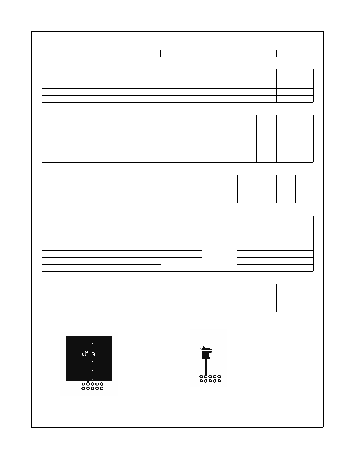
Dimensional Outline and Pad Layout
FDMC86102L N-Channel PowerTrench
®
MOSFET
©2010 Fairchild Semiconductor Corporation
FDMC86102L Rev.C
6
www.fairchildsemi.com
Page 7

TRADEMARKS
tm
®
tm
tm
The following includes registered and unregistered trademarks and service marks, owned by Fairchild Semiconductor an d/or its globa l subsidiaries, and is not
intended to be an exhaustive list of all such trademarks.
AccuPower™
Auto-SPM™
Build it Now™
CorePLUS™
CorePOWER™
CROSSVOLT™
CTL™
Current Transfer Logic™
DEUXPEED
Dual Cool™
EcoSPARK
EfficentMax™
®
®
ESBC™
®
Fairchild
Fairchild Semiconductor
FACT Quiet Series™
®
FACT
®
FAST
FastvCore™
FETBench™
FlashWriter
®
*
FPS™
®
F-PFS™
®
FRFET
Global Power Resource
Green FPS™
Green FPS™ e-Series™
Gmax™
GTO™
IntelliMAX™
ISOPLANAR™
MegaBuck™
MICROCOUPLER™
MicroFET™
MicroPak™
MicroPak2™
MillerDrive™
MotionMax™
Motion-SPM™
OptiHiT™
OPTOLOGIC
OPTOPLANAR
PDP SPM™
Power-SPM™
®
®
®
PowerTrench
PowerXS™
SM
Programmable Active Droop™
QFET
QS™
Quiet Series™
RapidConfigure™
Saving our world, 1mW/W/kW at a time™
SignalWise™
SmartMax™
SMART START™
SPM
STEALTH™
SuperFET
SuperSOT™-3
SuperSOT™-6
SuperSOT™-8
SupreMOS
SyncFET™
Sync-Lock™
®*
®
®
™
®
®
®
The Power Franchise
The Right Technology for Your Success™
TinyBoost™
TinyBuck™
TinyCalc™
TinyLogic
TINYOPTO™
TinyPower™
TinyPWM™
TinyWire™
TriFault Detect™
TRUECURRENT™*
μSerDes™
UHC
Ultra FRFET™
UniFET™
VCX™
VisualMax™
XS™
®
®
®
®
*Trademarks of System General Corporation, used under license by Fairchild Semiconductor.
DISCLAIMER
FAIRCHILD SEMICONDUCTOR RESERVES THE RIGHT TO MAKE CHANGES WITHOUT FURTHER NOTICE TO ANY PRODUCTS HEREIN TO IMPROVE
RELIABILITY, FUNCTION, OR DESIGN. FAIRCHILD DOES NOT ASSUME ANY LIABILITY ARISING OUT OF THE APPLICATION OR USE OF ANY
PRODUCT OR CIRCUIT DESCRIBED HEREIN; NEITHER DOES IT CONVEY ANY LICENSE UNDER ITS PATENT RIGHTS, NOR THE RIGHTS OF OTHERS.
THESE SPECIFICATIONS DO NOT EXPAND THE TERMS OF FAIRCHILD’S WORLDWIDE TERMS AND CONDITIONS, SPECIFICALLY THE WARRANTY
THEREIN, WHICH COVERS THESE PRODUCTS.
FDMC86102L N-Channel PowerTrench
®
MOSFET
LIFE SUPPORT POLICY
FAIRCHILD’S PRODUCTS ARE NOT AUTHORIZED FOR USE AS CRITICAL COMPONENTS IN LIFE SUPPORT DEVICES OR SYSTEMS WITHOUT THE
EXPRESS WRITTEN APPROVAL OF FAIRCHILD SEMICONDUCTOR CORPORATION.
As used here in:
1. Life support devices or systems are devices or systems which, (a) are
intended for surgical implant into the body or (b) support or sustain life,
and (c) whose failure to perform when properly used in accordance with
instructions for use provided in the labeling, can be reasonably
expected to result in a significant injury of the user.
ANTI-COUNTERFEITING POLICY
Fairchild Semiconductor Corporation’s Anti-Counterfeiting Policy. Fairchild’s Anti-Counterfeiting Policy is also stated on our external website,
www.Fairchildsemi.com, under Sales Support
Counterfeiting of semiconductor parts is a growing problem in the in dustry. All manufactures of semiconductor products are experi encing counterfeiting of their
parts. Customers who inadvertently purchase counterfeit part s experi ence ma ny pr oblems such as lo ss of brand r eput ation, sub stan dard perfor mance, failed
application, and increased cost of production and manufacturing delays. Fairchild is taking strong measures to protect ourselves and our customers from the
proliferation of counterfeit parts. Fairchild strongly encourages customers to purchase Fairchild part s either di rectly from Fairchild or from Authorized Fairchild
Distributors who are listed by country on our web page cited above. Products customers buy either from Fairchild directly or from Authorized Fairchild
Distributors are genuine parts, have full traceability, meet Fai r child’s quality standards for handing and storage and provide access to Fairchild’s full range of
up-to-date technical and product information. Fairchild and our Authorized Distributors will stand behind all warranties and will appropriately address and
warranty issues that may arise. Fairchild will not provide any warranty coverage or other assistance for parts bought from Unauthorized Sources. Fairchild is
.
2. A critical component in any component of a life support, device, or
system whose failure to perform can be reasonably expected to cause
the failure of the life support device or system, or to affect its safety or
effectiveness.
committed to combat this global problem and encourage our customers to do their part in stopping this practice by buying direct o r from authorized distr ibutors.
PRODUCT STATUS DEFINITIONS
Definition of Terms
Datasheet Identification Product Status Definition
Advance Information Formative / In Design
Preliminary First Production
No Identification Needed Full Production
Obsolete Not In Production
Datasheet contains the design specifications for product development. Specifications
may change in any manner without notice.
Datasheet contains preliminary data; supplementary data will be published at a later
date. Fairchild Semiconductor reserves the right to make changes at any ti me without
notice to improve design.
Datasheet contains final specifications. Fairchild Semiconductor reserves the right to
make changes at any time without notice to improve the design.
Datasheet contains specifications on a product that is discontinued by Fairchild
Semiconductor. The datasheet is for reference information only.
Rev. I51
©2010 Fairchild Semiconductor Corporation 7 www.fairchildsemi.com
FDMC86102L Rev.C
 Loading...