

Page 1
FDMF6730
PWM
CONTROLLER
LDO O UT
LDO E NABLE
LDO 5V OUT
PW M OUT
VIN
VOUT
DR IVE LS
DR IVE HS
LDO ADJ
LDO OUT
LDO EN
LDO 5V
VC C VIN
BOO T
VS WH
PG ND
LDR V
G_ PASS
D_P ASS
S_P ASSCS_ PROG
CS_ OUT
CG ND
FDMF6730
PWM
CONTROLLER
LDO O UT
LDO E NABLE
LDO 5V OUT
PW M OUT
VIN
VOUT
DR IVE LS
DR IVE HS
LDO ADJ
LDO OUT
LDO EN
LDO 5V
VC C VIN
BOO T
VS WH
PG ND
LDR V
G_ PASS
D_P ASS
S_P ASSCS_ PROG
CS_ OUT
CG ND
FDMF6730
Driver plus FET Multi-chip Module
FDMF6730 Driver plus FET Multi-chip Module
August 2008
Features
Over 95% efficiency
Internal 5V regulator for gate drive
6V-16V input range
1MHz max operating frequency
SMOD operation capability for light load efficiency
5A current capability (10A with PASS FET)
Current limit set by R
sensing to minimize power losses
DSON
Integrated bootstrap diode
Applications
Ultra Mobile PC
Notebook Computers
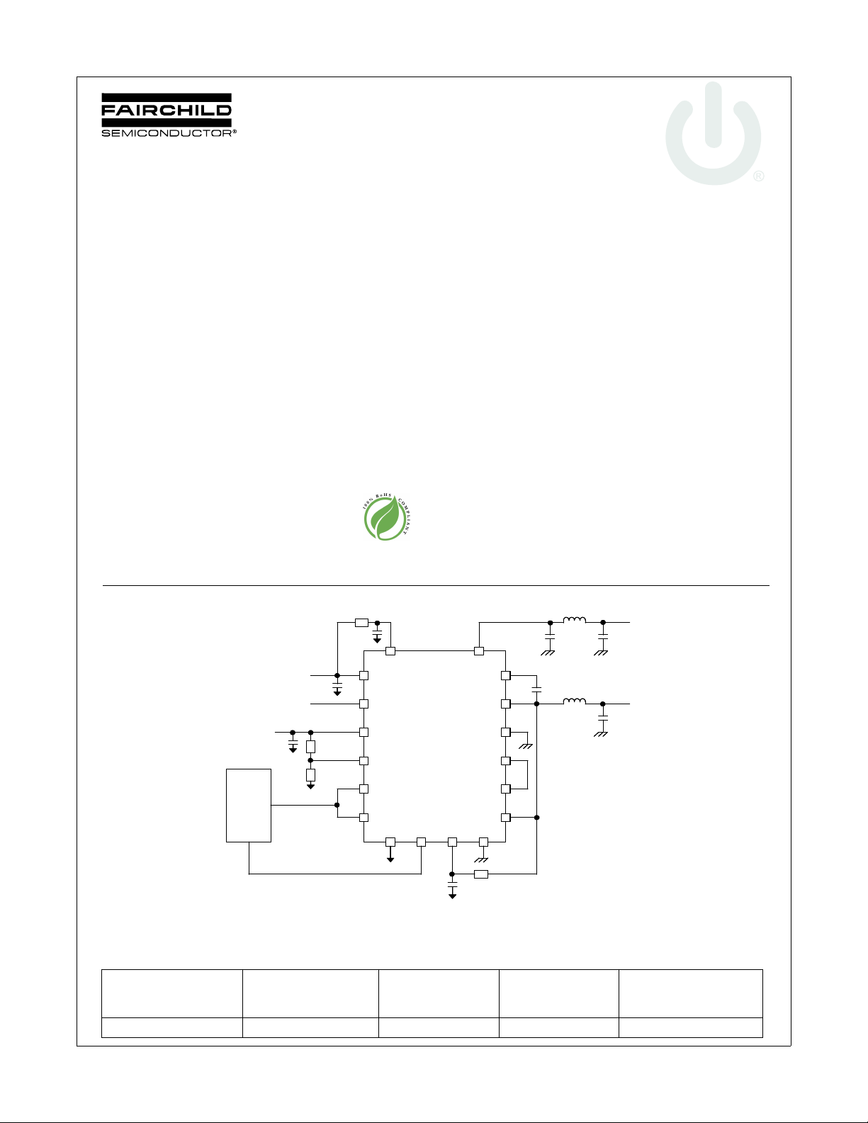
Typical Application
General Description
The FDMF6730 is a high efficiency Driver plus MOSFET power
stage solution optimized for Ultra Mobile PC (UMPC) system
power voltage supplies. It is fully compliant with the Intel UltraMobile Driver MOS (uDrMOS) Specification. The MOSFETs and
driver have been optimized to perform with high efficiency at
light and medium loads, ideal for compact PC devices.
The internal driver IC integrates two highly efficient LDOs for
internal gate-drive and external circuitry. The bootstrap diode is
also integrated within the IC. When operating with a single low
side MOSFET the uDrMOS module is capable of delivering up
to 5A of continuous current. The PASS transistor may be easily
routed in parallel with the low side MOSFET to provide up to
10A. The module also incorporates an over current protection
flag from an R
The device comes in a 6X6 Power QFN package for improved
thermal performance.
current sense architecture.
DSON
Ordering Information
©2008 Fairchild Semiconductor Corporation
Part
FDMF6730 10 6-16 1000 FDMF6730
FDMF6730 Rev. D2
Current Rating
Max
[A]
Figure 1. Power Train Application Circuit
Input Voltage
Typical
[V]
Frequency
Max
[KHz]
1
Device
Marking
www.fairchildsemi.com
Page 2
Functional Block Diagram
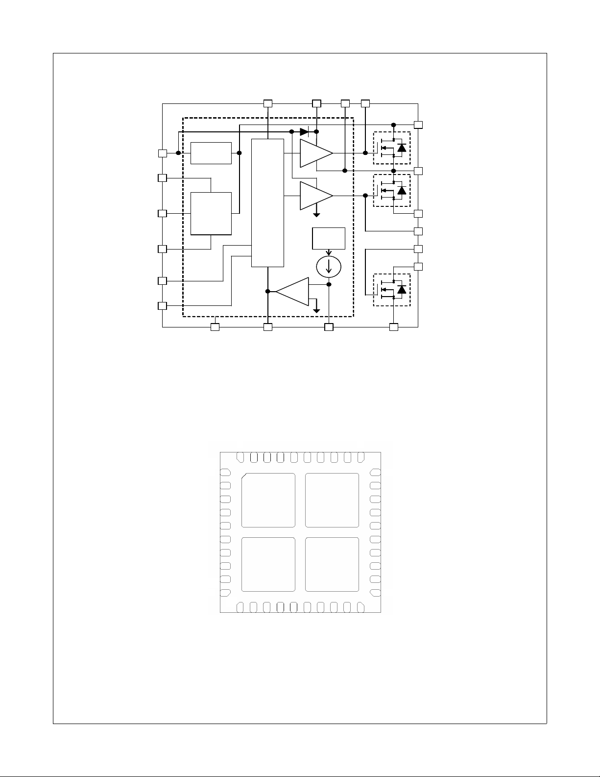
Figure 2. Functional Block Diagram
5V Reg
LD O
Ad just
OC P
Current
Tr im min g
VCC BOOT PHASE
VIN
VSW H
PGND
LD RV
G_PASS
D_PA S S
HD RV
S_PASSCS_P R O GCS _OUTCGND
DRIV E _ LS
DRIV E _ H S
LD O _ADJ
LD O_OUT
LD O _EN
LD O _5V
5V Reg
LD O
Ad just
OC P
Current
Tr im min g
VCC BOOT PHASE
VIN
VSW H
PGND
LD RV
G_PASS
D_PA S S
HD RV
S_PASSCS_P R O GCS _OUTCGND
DRIV E _ LS
DRIV E _ H S
LD O _ADJ
LD O_OUT
LD O _EN
LD O _5V
Figure 3. 6mm X 6mm, 40L MLP Bottom View
PGND
VSWH
VSWH
VSWH
VSWH
VIN
VIN
VIN
VIN
VIN
10
PGND
PGND
PGND
LDRV
VSWH
D_PASS
G_PASS
S_PASS
S_PASS
S_PASS
31
40
1
A
(VSWH)
S_PASS
NC
D_PASS
CS_PROG
CS_OUT
VCC
CGND
DRIVE_HS
DRIVE_LS
LDO_EN
2130
VIN
VIN
HDRV
CGND
PHASE
BOOT
LDO_5V
LDO_OUT
LDO_ADJ
20
11
VIN
B
(VIN)
D
(D_PASS)
C
(CGND)
PGND
VSWH
VSWH
VSWH
VSWH
VIN
VIN
VIN
VIN
VIN
10
PGND
PGND
PGND
LDRV
VSWH
D_PASS
G_PASS
S_PASS
S_PASS
S_PASS
31
40
1
A
(VSWH)
S_PASS
NC
D_PASS
CS_PROG
CS_OUT
VCC
CGND
DRIVE_HS
DRIVE_LS
LDO_EN
2130
VIN
VIN
HDRV
CGND
PHASE
BOOT
LDO_5V
LDO_OUT
LDO_ADJ
20
11
VIN
B
(VIN)
D
(D_PASS)
C
(CGND)
FDMF6730 Driver plus FET Multi- chip Module
Pin Configuration
FDMF6730 Rev. D2
2
www.fairchildsemi.com
Page 3
Pin Description
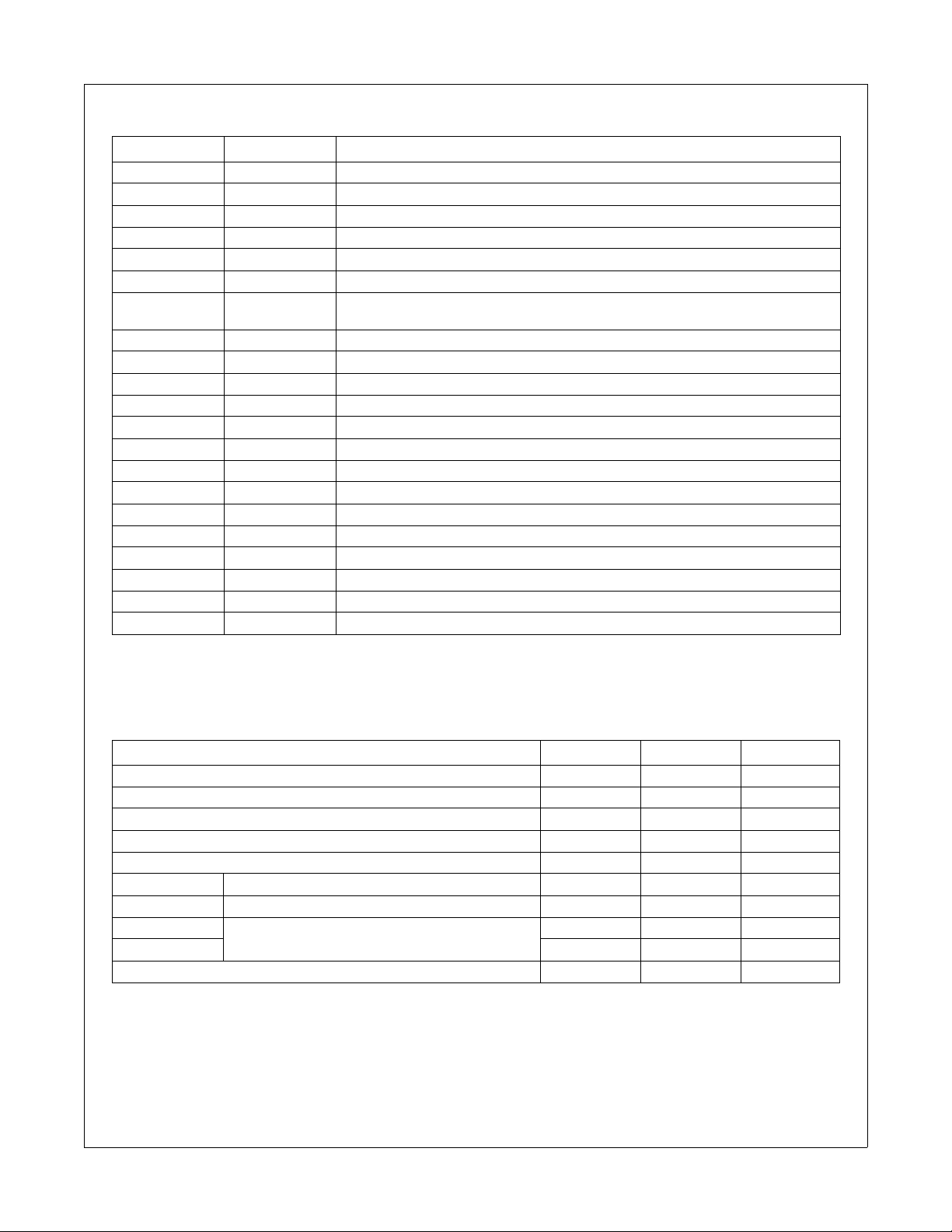
Pin Name Function
1, 38 - 40 PGND Low Side FET Source Pin. Connect to GND
2 - 5, 36, A VSWH Switch Node Pin. Low Side FET Drain pin. Electrically shorted to PHASE pin
6 - 12,14,B VIN Input Voltage Pin. Input voltage for buck converter
13 HDRV HDRV pin. High Side driver output. Connected to High Side FET gate pin.
15, 24, C CGND IC Ground. Ground return for driver IC.
16 PHASE Switch Node Pin for easy bootstrap capacitor routing. Electrically shorted to VSWH pin.
17 BOOT Bootstrap Supply Input Pin. Provides voltage supply to high-side MOSFET driver. Connect
bootstrap capacitor.
18 LDO_5V 5V Internal LDO Output.
19 LDO_OUT Adjustable LDO Output.
20 LDO_ADJ LDO Adjust Input. Connect to external voltage divider to adjust LDO output.
21 LDO_EN Adjustable LDO Enable Pin. 1 = Enable, 0 = Disable
22 DRIVE_LS Low Side PWM Input. Connect to PWM controller.
23 DRIVE_HS High Side PWM Input. Connect to PWM controller.
25 VCC Driver VCC. Connect to 5V.
26 CS_OUT Current Sense Output. 1 = Over-current Fault, 0 = No Fault.
27 CS_PROG Current Sense Program.
28, 35, D D_PASS Pass FET Drain Pin. Connect to VSWH pad for higher output current.
29 NC No Connect. This pin must be floated. Must not be connected to any pin.
30-33 S_PASS Pass FET Source Pin. Connect to PGND pad for higher output current.
34 G_PASS Pass FET Gate Pin. Connect to LDRV pin for higher output current.
37 LDRV LDRV pin. Low Side driver output. Connect to G_PASS pin for higher output current.
FDMF6730 Driver plus FET Multi- chip Module
Absolute Maximum Rating
Stresses exceeding the absolute maximum rating may damage the device. The device may not function or be operable above the
recommended operating conditions and stressing these parts to these levels is not recommended. In addition, extended exposure to
stresses above the recommended operating conditions may affect the device reliability. The absolute maximum rating are stress ratings only.
Parameter Min. Max. Units
VCC, Drive_LS, Drive_HS, LDO_EN, CS_Prog, CS_Out to GND -0.3 6 V
VIN to PGND -0.3 20 V
BOOT to VSWH -0.3 6 V
VSWH to PGND -1.0 27 V
BOOT to PGND -0.3 27 V
I
O(AV)
I
O(PK)
R
θJPCB
P
T
Operating and Storage Junction Temperature Range -55 150 °C
Note 1: Package power dissipation based on 4 layer, 2 square inch, 2 oz. copper pad. R
thermal resistance with PCB temperature referenced at VSWH pin.
VIN = 8.4V, VO = 3.3V, fSW = 1MHz, T
VIN = 8.4V, t
Junction to PCB Thermal Resistance note 1.
T
=130°C
PCB
= 10s 35 A
PULSE
= 130°C 10 A
PCB
5.5 °C/W
3.3 W
is the steady state junction to PCB
θJPCB
FDMF6730 Rev. D2
3
www.fairchildsemi.com
Page 4
Recommended Operating Range
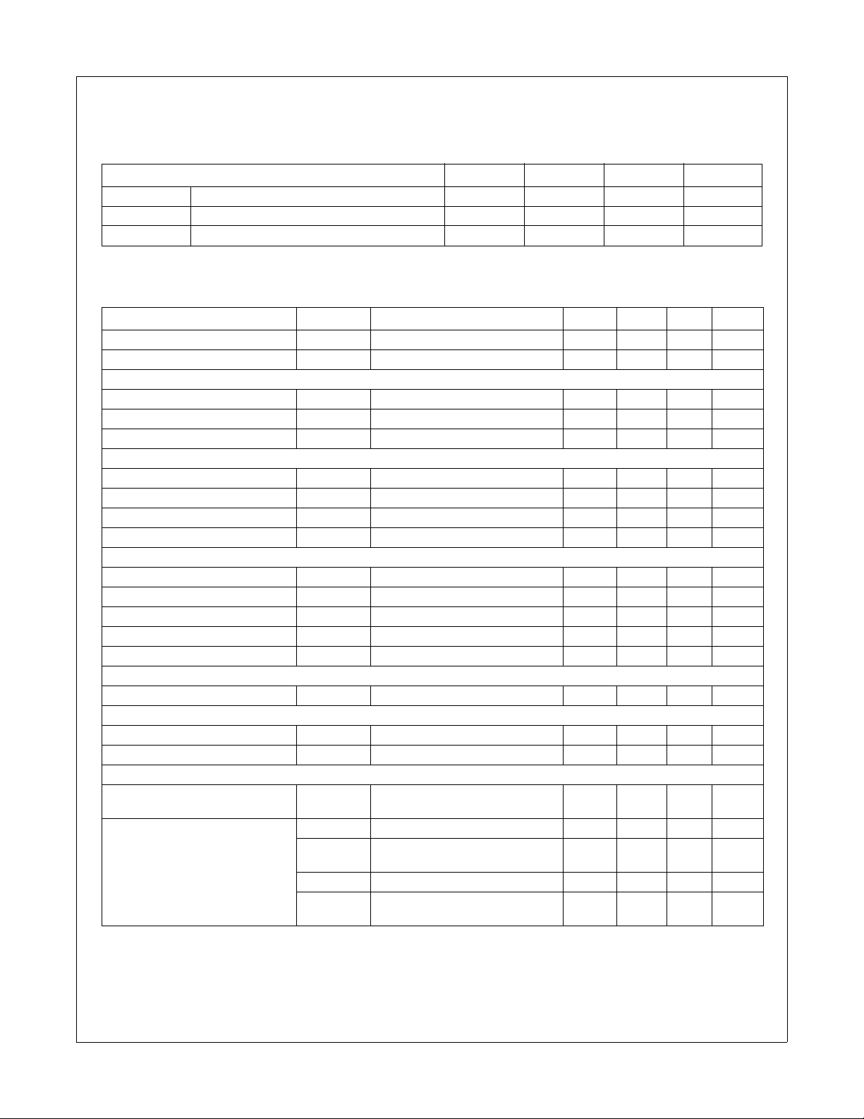
The recommended operating conditions table defines the conditions for actual device operation. These conditions are specified to
ensure optimal performance to the datasheet specification. Fairchild does not recommend exceeding them or designing to absolute
maximum ratings.
Parameter Min. Typ. Max. Units
V
V
V
CC
IN
OUT
Control Circuit Supply Voltage 4.5 5 5.5 V
Output Stage Supply Voltage 6 8.4 16 V
Output Voltage 1.5 3.3 5 V
Electrical Characteristics
VIN = 8.4V, VCC = 5V, TA = 25°C unless otherwise noted
Parameter Symbol Conditions Min. Typ. Max. Units
Input Voltage Range V
Operating Quiescent Current 2 mA
Drive_HS, Drive_LS, LDO_EN Logic Inputs
High Level Input V
Low Level Input V
Input Current -2 2 A
5V LDO
Output Voltage 4.7 5 5.3 V
Line Regulation 6V < VIN < 16V 5 mV
Load Regulation 5mA < I
Short Circuit Current Limit 100 180 mA
Adjustable LDO
Adjust Voltage V
Line Regulation 6V < VIN < 16V 3 mV
Load Regulation 5mA < I
Short Circuit Current Limit 100 180 mA
Adjust Input Bias Current 0.2 A
Over Current Protection
CS_Prog Current 30 40 50 A
Thermal Shutdown
Threshold 150
Hysteresis 19
Propagation Delay
250ns Timeout
IN
IH
IL
ADJ
t
TIMEOUT
t
DTHH
t
PDHL
t
DTLH
t
PDLL
.
6 16 V
2.4 V
0.4 V
< 100mA 75 mV
LOAD
0.58 0.6 0.62 V
< 100mA 11 mV
LOAD
o
o
VSWH = 2V, HDRV from HI to LO
and LDRV from LO to HI
LDRV going LO to VSWH going HI 30 ns
Drive_LS going HI to HDRV going
LO
VSWH going LO to LDRV going HI 20 ns
Drive_LS going LO to LDRV going
LO
250 ns
10 ns
10 ns
C
C
FDMF6730 Driver plus FET Multi- chip Module
FDMF6730 Rev. D2
4
www.fairchildsemi.com
Page 5
FDMF6730 Driver plus FET Multi-chip Module
Description of Operation
2-Bit PWM Input
The PWM input is composed of a high side drive and a low side
drive input which control the high side and low side FETs
respectively. They can also be setup to provide asynchronous
rectification (low FET off) and phase shutoff (both FETs off).
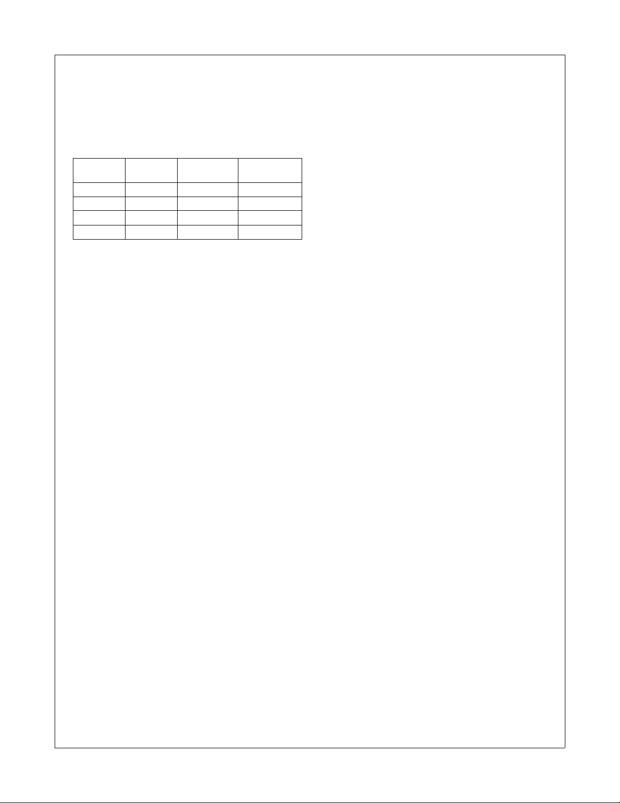
Truth Table
DRIVE_LS DRIVE_HS Low Side
0 0 OFF OFF
0 1 OFF ON
1 0 ON OFF
1 1 OFF OFF
PASS FET
One of the most unique features of the uDrMOS is the
integrated Pass FET. The pass FET can be easily routed in
parallel with the low side FET in order to provide up to 10A of
current. When not used as part of the DC-DC controller, it can
be used in other applications such as load switching, etc.
MOSFET
5V LDO
The uDrMOS conveniently incorporates a 5V LDO regulator to
drive the internal logic of the IC and gates of the internal
MOSFETs.
Adjustable LDO
Another feature of the part is the adjustable 100mA LDO. The
LDO output voltage is easily configured with a resistor divider.
Current Limit
The part also has current limit flag which is set by an internal
OCP topology.
High Side
MOSFET
Applications Section
Input Capacitor
A High frequency 4.7ceramic X5R must be connected directly
from V
Bootstrap Circuit
The bootstrap circuit uses a charge storage capacitor and an
external diode. A minimum of 0.1F high frequency capacitor
must be connected between the BOOT and PHASE pin. The
PHASE pin is already internally connected to the switch-node.
5V LDO
A minimum of 4.7F ceramic X5R type must be connected from
LDO_5V pin to GND to ensure stable operation and to provide
high frequency bypassing for low side driver. This LDO can
provide power to the internal logic circuitry and gate drivers via
a 10Ohm resistor. A high frequency 1F ceramic capacitor
must be placed from VCC to GND.
Adjustable LDO
A minimum of 10F ceramic X5R type must be connected close
from this pin to GND to insure stable operation for a range of
2.5V to 5V outputs. For output voltages of 0.6V to 2.5V the
minimum capacitance must be 22F ceramic type. A minimum
of 1mA load current must be connected from this pin to GND.
LDO_ADJ voltage 0.6V typical.
LDO_EN: Adjustable LDO enable pin (1= Enable, 0= Disable)
Over Current Protection
A resistor connected from the VSWH pin and this pin programs
the over current threshold point. CS_OUT is the output of an
internal current sense comparator which switches high when
the current in low side MOSFET exceeds a pre program level
set by the CS_PROG pin. This pin is low during normal
operation.
to GND
IN
FDMF6730 Rev. D2
5
www.fairchildsemi.com
Page 6
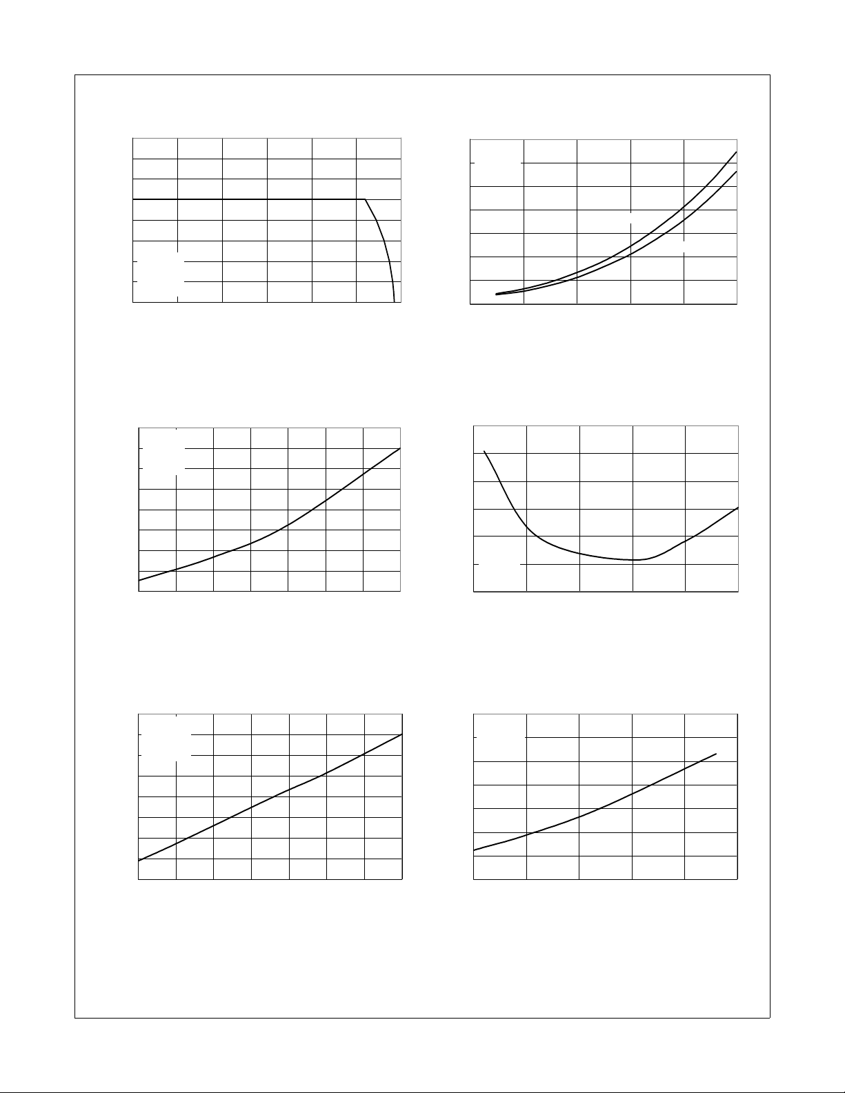
Typical Characteristics
0.0
0.5
1.0
1.5
2.0
2.5
3.0
3.5
0 2 4 6 8 10
I
LOAD
, A
P
LOSS
, W
VIN = 8.4V
V
OUT
= 3.3V
L = 2.2uH
FSW = 1MHz
FSW = 300KHz
0.86
0.88
0.90
0.92
0.94
0.96
0.98
1.00
1.02
300 400 500 600 700 800 900 1000
Switching Frequency, KHz
P
LOSS
(NORMALIZED)
VIN = 8.4V
V
OUT
= 3.3V
I
LOAD
= 10A
L = 2.2uH
0.96
0.98
1.00
1.02
1.04
1.06
1.08
6 8 10 12 14 16
Input Voltage, V
P
LOSS
(NORMALIZED)
V
OUT
= 3.3V
I
LOAD
= 10A
L = 2.2uH
FSW = 1MHz
0.80
0.85
0.90
0.95
1.00
1.05
1.10
1.15
1.20
1.5 2 2.5 3 3.5 4 4.5 5
Output Voltage, V
P
LOSS
(NORMALIZED)
VIN = 8.4V
I
LOAD
= 10A
L = 2.2uH
FSW = 1MHz
0
2
4
6
8
10
12
14
16
0 25 50 75 100 125 150
PCB Temperature, oC
I
LOAD
, A
VIN = 8.4V
V
OUT
= 3.3V
L = 2.2uH
FSW = 1MHz
0.85
0.90
0.95
1.00
1.05
1.10
1.15
1.20
1 1.5 2 2.5 3 3.5
Output Inductance, uH
P
LOSS
(NORMALIZED)
VIN = 8.4V
V
OUT
= 3.3V
I
LOAD
= 10A
FSW = 1MHz
Figure 4. Safe Operating Area Figure 5. Power Loss vs. Output Current
FDMF6730 Driver plus FET Multi-chip Module
Figure 6. Power Loss vs. Switching Frequency
FDMF6730 Rev. D2
Figure 8. Power Loss vs. Output Voltage Figure 9. Power Loss vs. Output Inductance
Figure 7. Power Loss vs. Input Voltage
Figure 7. Power Loss vs. Input Voltage
6
www.fairchildsemi.com
Page 7
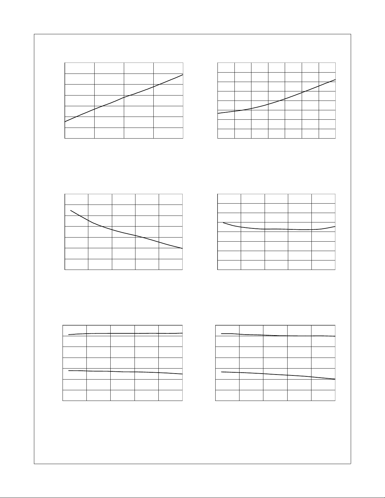
Typical Characteristics
0.52
0.54
0.56
0.58
0.60
0.62
0.64
0.66
4 4.5 5 5.5 6
Driver Supply Voltage, V
Supply Current, mA
0.52
0.54
0.56
0.58
0.60
0.62
0.64
0.66
-50 -10 30 70 110 150
Temperature, oC
Supply Current, mA
1.00
1.25
1.50
1.75
2.00
2.25
2.50
2.75
3.00
300 400 500 600 700 800 900 1000
Frequency, kHz
Supply Current, mA
1.2
1.3
1.4
1.5
1.6
1.7
1.8
1.9
-50 -10 30 70 110 150
Temperature, oC
Drive_LS Threshold Voltage, V
1.2
1.3
1.4
1.5
1.6
1.7
1.8
1.9
-50 -10 30 70 110 150
Temperature, oC
Drive_HS Threshold Voltage, V
1.20
1.23
1.25
1.28
1.30
1.33
1.35
1.38
1.40
-50 -10 30 70 110 150
Temperature, oC
LDO_EN Threshold Voltage, V
Figure 10. Supply Current vs. Driver Supply Figure 11. Supply Current vs. Frequency
FDMF6730 Driver plus FET Multi-chip Module
Figure 12. Supply Current vs. Temperature Figure 13. LDO_EN Threshold Voltage vs. Temperature
Figure 14. Driver_LS Threshold Voltage vs. Temperature Figure 15. Driver_HS Threshold Voltage vs. Temperature
FDMF6730 Rev. D2
7
www.fairchildsemi.com
Page 8
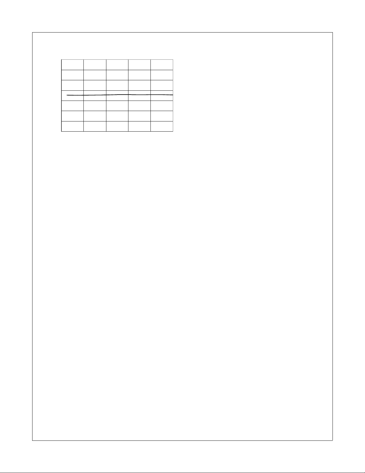
Typical Characteristics
37.5
38.0
38.5
39.0
39.5
40.0
40.5
41.0
-50 -10 30 70 110 150
Temperature, oC
CS_Prog Current, uA
Figure 16. CS_Prog Current vs. Temperature
FDMF6730 Driver plus FET Multi-chip Module
FDMF6730 Rev. D2
8
www.fairchildsemi.com
Page 9
11
21
31
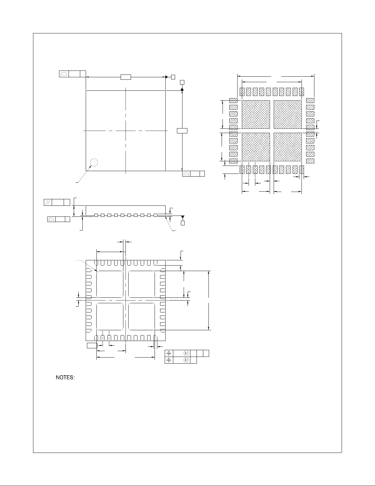
D. DRAWING FILE NAME: MLP40XREV1
(0.20)
(0.20)
(0.20)
0.80 MAX
0.10
C
0.08
C
C
(0.20)
SEATING PLANE
BOTTOM VIEW
SIDE VIEW
1
31
11
2.00? .10 (2X)
2.00? .10 (2X)
4.40? .10
4.40? .10
0.50
0.30
0.20~0.30
0.10 C A B
0.05 C
40X
40X
0.50
PIN #1 IDENT
1
RECOMMENDED LAND PATTERN
0.60
0.35
2.10
2.10
5.80
2.10
2.10
4.50
0.30
0.30
B. DIMENSIONS ARE IN MILLIMETERS.
C. DIMENSIONS AND TOLERANCES PER
A. DOES NOT FULLY CONFORM TO JEDEC REGISTRATION,
MO-220. DATED MAY/2005.
ASME Y14.5M, 1994
PIN #1 IDENT
6.00
6.00
0.10 C
B
2X
0.10 C
2X
TOP VIEW
0.05
0.00
0.50 TYP
(2.20)
A
Dimensional Outline and Pad layout
FDMF6730 Driver plus FET Multi-chip Module
FDMF6730 Rev. D2
9
www.fairchildsemi.com
Page 10
TRADEMARKS
tm
®
tm
tm
The following includes registered and unregistered trademarks and service marks, owned by Fairchild Semiconductor and/or its global subsidianries, and is
not intended to be an exhaustive list of all such trademarks.
Build it Now™
CorePLUS™
CorePOWER™
CROSSVOLT™
CTL™
Current Transfer Logic™
EcoSPARK
EfficentMax™
EZSWITCH™ *
™
Fairchild
®
®
Fairchild Semiconductor
FACT Quiet Series™
®
FACT
®
FAST
FastvCore™
FlashWriter® *
FPS™
F-PFS™
®
FRFET
Global Power Resource
Green FPS™
Green FPS™ e-Series™
SM
GTO™
IntelliMAX™
ISOPLANAR™
MegaBuck™
MICROCOUPLER™
MicroFET™
MicroPak™
®
MillerDrive™
MotionMax™
Motion-SPM™
OPTOLOGIC
OPTOPLANAR
®
®
®
PDP SPM™
Power-SPM™
PowerTrench
Programmable Active Droop™
QFET
QS™
®
®
Quiet Series™
RapidConfigure™
Saving our world, 1mW at a time™
SmartMax™
SMART START™
®
SPM
STEALTH™
SuperFET™
SuperSOT™-3
SuperSOT™-6
SuperSOT™-8
SupreMOS™
SyncFET™
The Power Franchise
TinyBoost™
TinyBuck™
®
TinyLogic
TINYOPTO™
TinyPower™
TinyPWM™
TinyWire™
®
UHC
Ultra FRFET™
UniFET™
VCX™
VisualMax™
®
®
* EZSWITCH™ and FlashWriter® are trademarks of System General Corporation, used under license by Fairchild Semiconductor.
DISCLAIMER
FAIRCHILD SEMICONDUCTOR RESERVES THE RIGHT TO MAKE CHANGES WITHOUT FURTHER NOTICE TO ANY PRODUCTS HEREIN TO IMPROVE
RELIABILITY, FUNCTION, OR DESIGN. FAIRCHILD DOES NOT ASSUME ANY LIABILITY ARISING OUT OF THE APPLICATION OR USE OF ANY
PRODUCT OR CIRCUIT DESCRIBED HEREIN; NEITHER DOES IT CONVEY ANY LICENSE UNDER ITS PATENT RIGHTS, NOR THE RIGHTS OF OTHERS.
THESE SPECIFICATIONS DO NOT EXPAND THE TERMS OF FAIRCHILD’S WORLDWIDE TERMS AND CONDITIONS, SPECIFICALLY THE WARRANTY
THEREIN, WHICH COVERS THESE PRODUCTS.
FDMF6730 Driver plus FET Multi-chip Module
LIFE SUPPORT POLICY
FAIRCHILD’S PRODUCTS ARE NOT AUTHORIZED FOR USE AS CRITICAL COMPONENTS IN LIFE SUPPORT DEVICES OR SYSTEMS WITHOUT THE
EXPRESS WRITTEN APPROVAL OF FAIRCHILD SEMICONDUCTOR CORPORATION.
As used herein:
1. Life support devices or systems are devices or systems which, (a) are
intended for surgical implant into the body or (b) support or sustain life,
and (c) whose failure to perform when properly used in accordance with
instructions for use provided in the labeling, can be reasonably
expected to result in a significant injury of the user.
ANTI-COUNTERFEITING POLICY
Fairchild Semiconductor Corporation’s Anti-Counterfeiting Policy. Farichild’s Anti-Counterfeiting Policy is also stated on our external website,
www.fairchildsemi.com, under Sales Support
.
2. A critical component in any component of a life support, device, or
system whose failure to perform can be reasonably expected to cause
the failure of the life support device or system, or to affect its safety or
effectiveness.
Counterfeiting of semiconductor parts is a growing problem in the industry. All manufactures of semiconductor products are experiencing counterfeiting of their
parts. Customers who inadvertently purchase counterfeit parts experience many problems such as loss of brand reputation, substandard performance, failed
application, and increased cost of production and manufacturing delays. Fairchild is taking strong measures to protect ourselves and our customers from the
proliferation of counterfeit parts. Farichild strongly encourages customers to purchase Farichild parts either directly from Fairchild or from Authorized Fairchild
Distributors who are listed by country on our web page cited above. Products customers buy either from fairchild directly or from Authorized Fairchild
Distributors are genuine parts, have full traceability, meet Fairchild’s quality standards for handing and storage and provide access to Farichild’s full range of
up-to-date technical and product information. Fairchild and our Authorized Distributors will stand behind all warranties and will appropriately address and
warranty issues that may arise. Fairchild will not provide any warranty coverage or other assistance for parts bought from Unauthorized Sources. Farichild is
committed to committed to combat this global problem and encourage our customers to do their part in stopping this practice by buying direct or from authorized
distributors.
PRODUCT STATUS DEFINITIONS
Definition of Terms
Datasheet Identification Product Status Definition
Advance Information Formative / In Design
Preliminary First Production
No Identification Needed Full Production
Obsolete Not In Production
Datasheet contains the design specifications for product development. Specifications
may change in any manner without notice.
Datasheet contains preliminary data; supplementary data will be published at a later
date. Fairchild Semiconductor reserves the right to make changes at any time without
notice to improve design.
Datasheet contains final specifications. Fairchild Semiconductor reserves the right to
make changes at any time without notice to improve the design.
Datasheet contains specifications on a product that is discontinued by Fairchild
Semiconductor. The datasheet is for reference information only.
Rev. I35
10
www.fairchildsemi.com
FDMF6730 Rev. D2
 Loading...