

Page 1
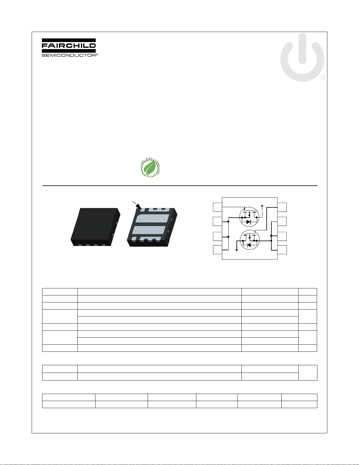
FDMC8030
D1
D2
S1
G1
S2
G2
Power 33
Pin 1
S1S1
S2S2
G2
S2
G1
S1
S2
S2
S1
S1
4
3
2
18
7
6
5
Bottom Drain1 Contact
Bottom D r a in2 Conta ct
Q2
Q1
Dual N-Channel Power Trench® MOSFET
40 V, 12 A, 10 mΩ
Features
Max r
Max r
Max r
Termination is Lead-free and RoHS Compliant
= 10 mΩ at VGS = 10 V, ID = 12 A
DS(on)
= 14 mΩ at VGS = 4.5 V, ID = 10 A
DS(on)
= 28 mΩ at VGS = 3.2 V, ID = 4 A
DS(on)
General Description
This device includes two 40V N-Channel MOSFETs in a dual
Power 33 (3 mm X 3 mm MLP) package. The package is
enhanced for exceptional thermal performance.
Applications
Battery Protection
Load Switching
Point of Load
FDMC8030 Dual N-Channel Power Trench
August 2011
®
MOSFET
MOSFET Maximum Ratings T
Symbol Parameter Ratings Units
V
DS
V
GS
I
D
E
AS
P
D
, T
T
J
STG
Thermal Characteristics
R
θJA
R
θJA
Package Marking and Ordering Information
Device Marking Device Package Reel Size Tape Width Quantity
FDMC8030 FDMC8030 Power 33 13 ’’ 12 mm 3000 units
©2011 Fairchild Semiconductor Corporation
FDMC8030 Rev.C
Drain to Source Voltage 40 V
Gate to Source Voltage (Note 4) ±12 V
Drain Current -Continuous TA = 25 °C (Note 1a) 12
-Pulsed 50
Single Pulse Avalanche Energy (Note 3) 21 mJ
Power Dissipation TA = 25 °C (Note 1a) 1.9
Power Dissipation T
Operating and Storage Junction Temperature Range -55 to +150 °C
Thermal Resistance, Junction to Ambient (Note 1a) 65
Thermal Resistance, Junction to Ambient (Note 1b) 155
= 25 °C unless otherwise noted
A
= 25 °C (Note 1b) 0.8
A
1
A
W
°C/W
www.fairchildsemi.com
Page 2
Electrical Characteristics T
= 25 °C unless otherwise noted
J
Symbol Parameter Test Conditions Min Typ Max Units
Off Characteristics
BV
ΔBV
ΔT
I
DSS
I
GSS
DSS
DSS
J
Drain to Source Breakdown Voltage ID = 250 μA, VGS = 0 V 40 V
Breakdown Voltage Temperature
Coefficient
Zero Gate Voltage Drain Current VDS = 32 V, V
Gate to Source Leakage Current, Forward VGS = 12 V, V
I
= 250 μA, referenced to 25 °C 19 mV/°C
D
= 0 V 1 μA
GS
= 0 V 100 nA
DS
On Characteristics
V
GS(th)
ΔV
ΔT
r
DS(on)
g
FS
GS(th)
J
Gate to Source Threshold Voltage VGS = VDS, ID = 250 μA 1.0 1.5 2.8 V
Gate to Source Threshold Voltage
Temperature Coefficient
Static Drain to Source On Resistance
I
= 250 μA, referenced to 25 °C -5 mV/°C
D
= 10 V, ID = 12 A 8 10
V
GS
V
= 4.5 V, ID = 10 A 10 14
GS
= 3.2 V, ID = 4 A 19 28
V
GS
= 10 V, ID = 12 A
V
GS
T
= 125 °C
J
13 16
Forward Transconductance VDD = 5 V, ID = 12 A 57 S
Dynamic Characteristics
C
iss
C
oss
C
rss
R
g
Input Capacitance
Output Capacitance 321 430 pF
Reverse Transfer Capacitance 20 30 pF
= 20 V, VGS = 0 V
V
DS
f = 1MHz
Gate Resistance 0.9 2.5 Ω
1462 1975 pF
FDMC8030 Dual N-Channel Power Trench
mΩ
®
MOSFET
Switching Characteristics
t
d(on)
t
r
t
d(off)
t
f
Q
Q
Q
g(TOT)
gs
gd
Turn-On Delay Time
Rise Time 310ns
Turn-Off Delay Time 19 33 ns
Fall Time 310ns
Total Gate Charge VGS = 0 V to 10 V
Total Gate Charge V
Gate to Source Charge 2.8 nC
Gate to Drain “Miller” Charge 2.5 nC
= 20 V, ID = 12 A
V
DD
V
= 10 V, R
GS
= 0 V to 5 V 12 17 nC
GS
GEN
Drain-Source Diode Characteristics
V
SD
t
rr
Q
rr
NOTES:
is determined with the device mounted on a 1 in2 pad 2 oz copper pad on a 1.5 x 1.5 in. board of FR-4 material. R
1. R
θJA
the user's board design.
Source to Drain Diode Forward Voltage V
Reverse Recovery Time
Reverse Recovery Charge 9 18 nC
a. 65 °C/W when mounted on
2
pad of 2 oz copper
a 1 in
= 0 V, IS = 12 A (Note 2) 0.83 1.2 V
GS
= 12 A, di/dt = 100 A/μs
I
F
= 6 Ω
V
DD
I
= 12 A
D
= 20 V
713ns
21 30 nC
25 40 ns
is guaranteed by design while R
θJC
b.155 °C/W when mounted on
a minimum pad of 2 oz copper
is determined by
θCA
2. Pulse Test: Pulse Width < 300 μs, Duty cycle < 2.0 %.
3. E
of 21 mJ is based on starting TJ = 25 oC, L = 0.3 mH, IAS = 12 A, VDD = 36 V, VGS = 10 V. 100% tested at L = 3 mH, IAS = 5 A.
AS
4. As an N-ch device, the negative V
©2011 Fairchild Semiconductor Corporation
FDMC8030 Rev.C
rating is for low duty cycle pulse occurence only. No continuous rating is implied.
gs
2
www.fairchildsemi.com
Page 3
FDMC8030 Dual N-Channel Power Trench
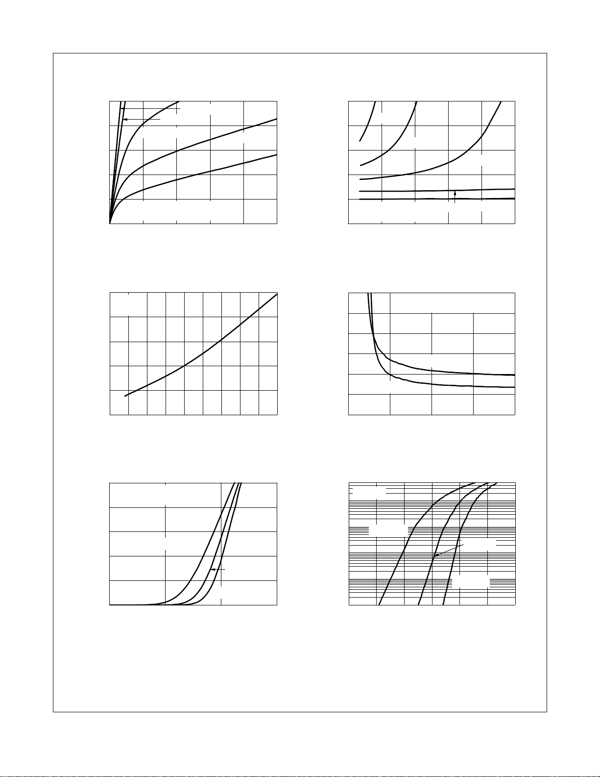
012345
0
10
20
30
40
50
VGS = 3 V
VGS = 10 V
VGS = 3.5 V
PULSE DURATION = 80μs
DUTY CYCLE = 0.5%MAX
VGS = 4.5 V
VGS = 3.2 V
I
D
, DRAIN CURRENT (A)
V
DS
, DRAIN TO SOURCE VOLTA GE (V)
0 1020304050
0
1
2
3
4
5
V
GS
= 10 V
PULSE DURATION = 80μs
DUTY CYCLE = 0.5%MAX
NORMALIZED
DRAIN TO SOURCE ON-RESISTA NCE
I
D
, DRAIN CURRENT(A)
V
GS
= 3.5 V
VGS =3.2 V
VGS = 3 V
V
GS
= 4.5 V
-75 -50 -25 0 25 50 75 100 125 150
0.6
0.8
1.0
1.2
1.4
1.6
ID = 12 A
V
GS
= 10 V
NORMALIZED
DRAIN TO SOURCE ON-RESIST ANCE
T
J
, JUNCTION TEMPERATURE (
o
C)
246810
0
5
10
15
20
25
30
ID = 12 A
TJ = 25 oC
TJ = 125 oC
V
GS
, GATE TO SOURCE V OLTAGE (V )
r
DS(on)
,
DRAIN TO
SOURCE ON-RESISTANCE
(mΩ)
PULSE DURATION = 80μs
DUTY CYCLE = 0.5%MAX
1234
0
10
20
30
40
50
TJ = 25 oC
TJ = -55 oC
V
DS
= 5 V
PULSE DURATION = 80μs
DUTY CYCLE = 0.5%MAX
TJ = 150 oC
I
D
, DRAIN CURRENT (A)
VGS, GATE TO SOURCE VOLTAGE (V)
0.0 0.2 0.4 0.6 0.8 1.0 1.2
0.001
0.01
0.1
1
10
50
TJ = -55 oC
TJ = 25 oC
TJ = 150 oC
V
GS
= 0 V
I
S
, REVERSE DRAIN CURRENT (A)
VSD, BODY DIODE FORWARD VOLTAGE (V)
Typical Characteristics T
Figure 1.
On-Region Characteristics Figure 2.
= 25°C unless otherwise noted
J
Nor mal ize d On -Re sis tan ce
vs Drain Current and Gate Voltage
®
MOSFET
Figur e 3. Norma liz ed On- Res is tan ce
vs Junction Temperature
©2011 Fairchild Semiconductor Corporation
FDMC8030 Rev.C
Figure 5. Transfer Characteristics
Figure 4.
On-Resist ance vs Gate to
Source Voltage
Figure 6.
Source to Drain Dio de
Forward Voltage vs Source Current
3
www.fairchildsemi.com
Page 4

FDMC8030 Dual N-Channel Power Trench
0 5 10 15 20
0
2
4
6
8
10
ID = 12 A
VDD = 15 V
V
DD
= 20 V
V
GS
, GATE TO SOURCE VOLTAGE(V)
Qg, GATE CHARGE(nC)
VDD = 25 V
0.1 1 10 40
1
10
100
1000
2000
f = 1 MHz
V
GS
= 0 V
CAPACITANCE (pF)
VDS, DRAIN TO SOURCE VOLTAGE (V)
C
rss
C
oss
C
iss
0.001 0.01 0.1 1 1 0 20
1
10
30
TJ = 100 oC
TJ = 25 oC
TJ = 125 oC
tAV, TIME IN AVALANCHE(ms)
I
AS
, AVALANCHE CURRENT(A)
0.01 0.1 1 10 100200
0.01
0.1
1
10
60
100 μs
10 ms
10 s
100 ms
DC
1 s
1 ms
I
D
, DRAIN CURRENT (A)
VDS, DRAIN to SOURCE VOLTAGE (V)
THIS AREA IS
LIMITED BY r
DS(on)
SINGLE PULSE
T
J
= MAX RATED
R
θJA
= 155
o
C/W
T
A
= 25
o
C
10
-4
10
-3
10
-2
10
-1
110
100 1000
0.1
1
10
100
1000
P
(PK)
, PEAK TRANSIENT POWER (W)
SINGLE PULSE
R
θJA
= 155 oC/W
T
A
= 25 oC
t, PULSE WIDTH (sec)
Typical Characteristics T
Figure 7.
Gate Charge Characteristics
= 25°C unless otherwise noted
J
Figure 8.
Cap acit anc e vs D rain
to Source Voltage
®
MOSFET
Figure 9.
Unc l ampe d Ind u cti v e
Switching Capability
©2011 Fairchild Semiconductor Corporation
FDMC8030 Rev.C
Figure 10.
Operating Area
Figure 11. Single Pulse Maximum Power Dissipation
4
Forward Bias Safe
www.fairchildsemi.com
Page 5

FDMC8030 Dual N-Channel Power Trench
10
-4
10
-3
10
-2
10
-1
110
100 1000
0.001
0.01
0.1
1
SINGLE PULSE
R
θJA
= 155 oC/W
DUTY CYCLE-DESCENDING O RD ER
NORMALIZED THERMAL
IMPEDANCE,
Z
θJA
t, RECTANGULAR PU L SE D U R ATION (sec)
D = 0.5
0.2
0.1
0.05
0.02
0.01
2
P
DM
t
1
t
2
NOTES:
DUTY FACTOR: D = t
1/t2
PEAK TJ = PDM x Z
θJA
x R
θJA
+ T
A
Typical Characteristics T
Figure 12. Junction-to-Ambient Transient Thermal Response Curve
= 25°C unless otherwise noted
J
®
MOSFET
©2011 Fairchild Semiconductor Corporation
FDMC8030 Rev.C
5
www.fairchildsemi.com
Page 6

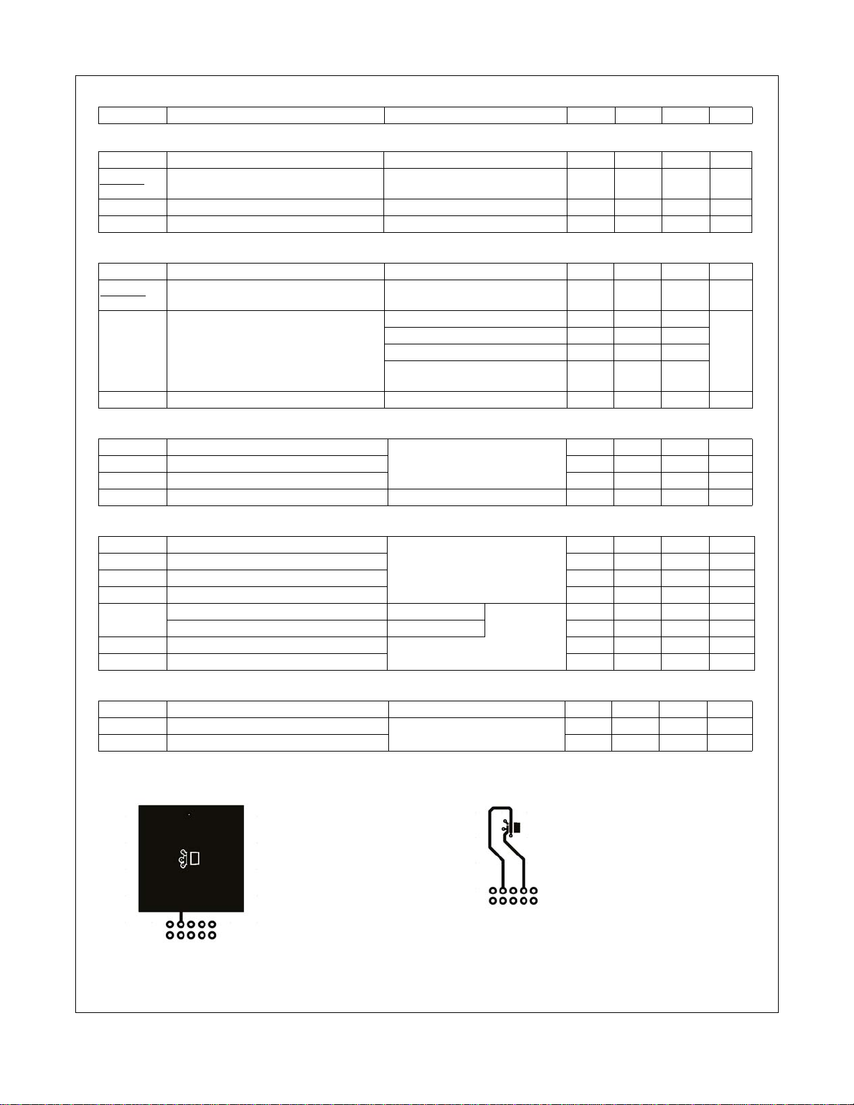
Dimensional Outline and Pad Layout
FDMC8030 Dual N-Channel Power Trench
®
MOSFET
©2011 Fairchild Semiconductor Corporation
FDMC8030 Rev.C
6
www.fairchildsemi.com
Page 7

TRADEMARKS
tm
®
tm
™
tm
The following includes registered and unregistered trademarks and service marks, owned by Fairchild Semi conductor and/or its glob al subsidiaries, and is not
intended to be an exhaustive list of all such trademarks.
2Cool™
AccuPower™
Auto-SPM™
AX-CAP™*
®
BitSiC
Build it Now™
CorePLUS™
CorePOWER™
CROSSVOLT™
CTL™
Current Transfer Logic™
DEUXPEED
Dual Cool™
EcoSPARK
EfficentMax™
ESBC™
Fairchild
Fairchild Semiconductor
FACT Quiet Series™
FACT
FAST
FastvCore™
FETBench™
®
®
®
®
®
®
FlashWriter
FPS™
F-PFS™
FRFET
Global Power Resource
Green FPS™
Green FPS™ e-Series™
Gmax™
GTO™
IntelliMAX™
ISOPLANAR™
MegaBuck™
MICROCOUPLER™
MicroFET™
MicroPak™
MicroPak2™
MillerDrive™
MotionMax™
Motion-SPM™
mWSaver™
OptiHiT™
OPTOLOGIC
OPTOPLANAR
®
*
®
®
®
®
PDP SPM™
Power-SPM™
PowerTrench
PowerXS™
SM
Programmable Active Droop™
QFET
QS™
Quiet Series™
RapidConfigure™
Saving our world, 1mW/W/kW at a time™
SignalWise™
SmartMax™
SMART START™
SPM
STEALTH™
SuperFET
SuperSOT™-3
SuperSOT™-6
SuperSOT™-8
SupreMOS
SyncFET™
Sync-Lock™
®
®
®
®
®
®*
The Power Franchise
The Right Technology for Your Success™
TinyBoost™
TinyBuck™
TinyCalc™
®
TinyLogic
TINYOPTO™
TinyPower™
TinyPWM™
TinyWire™
®
TranSiC
TriFault Detect™
TRUECURRENT
μSerDes™
®
UHC
Ultra FRFET™
UniFET™
VCX™
VisualMax™
XS™
®
®
®
*
FDMC8030 Dual N-Channel Power Trench
®
MOSFET
*Trademarks of System General Corporation, used under license by Fairchild Semiconductor.
DISCLAIMER
FAIRCHILD SEMICONDUCTOR RESERVES THE RIGHT TO MAKE CHANGES WITHOUT FURTHER NOTICE TO ANY PRODUCTS HEREIN TO IMPROVE
RELIABILITY, FUNCTION, OR DESIGN. FAIRCHILD DOES NOT ASSUME ANY LIABILITY ARISING OUT OF THE APPLICATION OR USE OF ANY
PRODUCT OR CIRCUIT DESCRIBED HEREIN; NEITHER DOES IT CONVEY ANY LICENSE UNDER ITS PATENT RIGHTS, NOR THE RIGHTS OF OTHERS.
THESE SPECIFICATIONS DO NOT EXPAND THE TERMS OF FAIRCHILD’S WORLDWIDE TERMS AND CONDITIONS, SPECIFICALLY THE WARRANTY
THEREIN, WHICH COVERS THESE PRODUCTS.
LIFE SUPPORT POLICY
FAIRCHILD’S PRODUCTS ARE NOT AUTHORIZED FOR USE AS CRITICAL COMPONENTS IN LIFE SUPPORT DEVICES OR SYSTEMS WITHOUT THE
EXPRESS WRITTEN APPROVAL OF FAIRCHILD SEMICONDUCTOR CORPORATION.
As used here in:
1. Life support devices or systems are devices or systems which, (a) are
intended for surgical implant into the body or (b) support or sustain life,
and (c) whose failure to perform when properly used in accordance with
instructions for use provided in the labeling, can be reasonably
expected to result in a significant injury of the user.
ANTI-COUNTERFEITING POLICY
Fairchild Semiconductor Corporation’s Anti-Counterfeiting Policy. Fairchild’s Anti-Counterfeiting Policy is also stated on our external website,
www.Fairchildsemi.com, under Sales Support
Counterfeiting of semiconductor parts is a growing problem in the industry. All ma nufactures of semiconductor products are exper iencing counterfeiting of their
parts. Customers who inadvertently purchase counterfeit parts experience many proble ms su ch as loss of brand repu tation , substa ndard pe rfo rmance, f aile d
application, and increased cost of production and manufacturing delays. Fairchild is takin g stron g measures to protect ourselves and our customers from th e
proliferation of counterfeit parts. Fairchild str ongly encourages customers t o purchase Fairchild par ts either d irectly from Fairchild o r from Authorized Fairchild
Distributors who are listed by country on our web page cited above. Products customers buy either from Fairchild directly or from Authorized Fairchild
Distributors are genuine parts, have full traceability, meet Fairchild’s quality standards for handing and storage and provide access to Fairchild’s full range of
up-to-date technical and product information. Fairchild and our Authorized Distributors will stand behind all warranties and will appropriately address and
warranty issues that may arise. Fairchild will not provide any warranty coverage or other assistance for parts bought from Unauthorized Sources. Fairchild is
committed to combat this global problem and encourage our customers to do their part in stopping t his practice by buying direct or from authorized distributor s.
PRODUCT STATUS DEFINITIONS
Definition of Terms
.
2. A critical component in any component of a life support, device, or
system whose failure to perform can be reasonably expected to ca use
the failure of the life support device or system, or to affect its safety or
effectiveness.
Datasheet Identification Product Status Definition
Advance Information Formative / In Design
Preliminary First Production
No Identification Needed Full Production
Obsolete Not In Production
©2011 Fairchild Semiconductor Corporation
FDMC8030 Rev.C
Datasheet contains the design specifications fo r product development. Specifications
may change in any manner without notice.
Datasheet contains preliminary data; supplementary data will be published at a later
date. Fairchild Semiconductor reserves the right to make changes at any time without
notice to improve design.
Datasheet contains final specifications. Fairchild Semiconductor reserves the right to
make changes at any time without notice to improve the design.
Datasheet contains specifications on a product that is discontinued by Fairchild
Semiconductor. The datasheet is for reference information only.
7
www.fairchildsemi.com
Rev. I55
 Loading...