

Page 1
tm
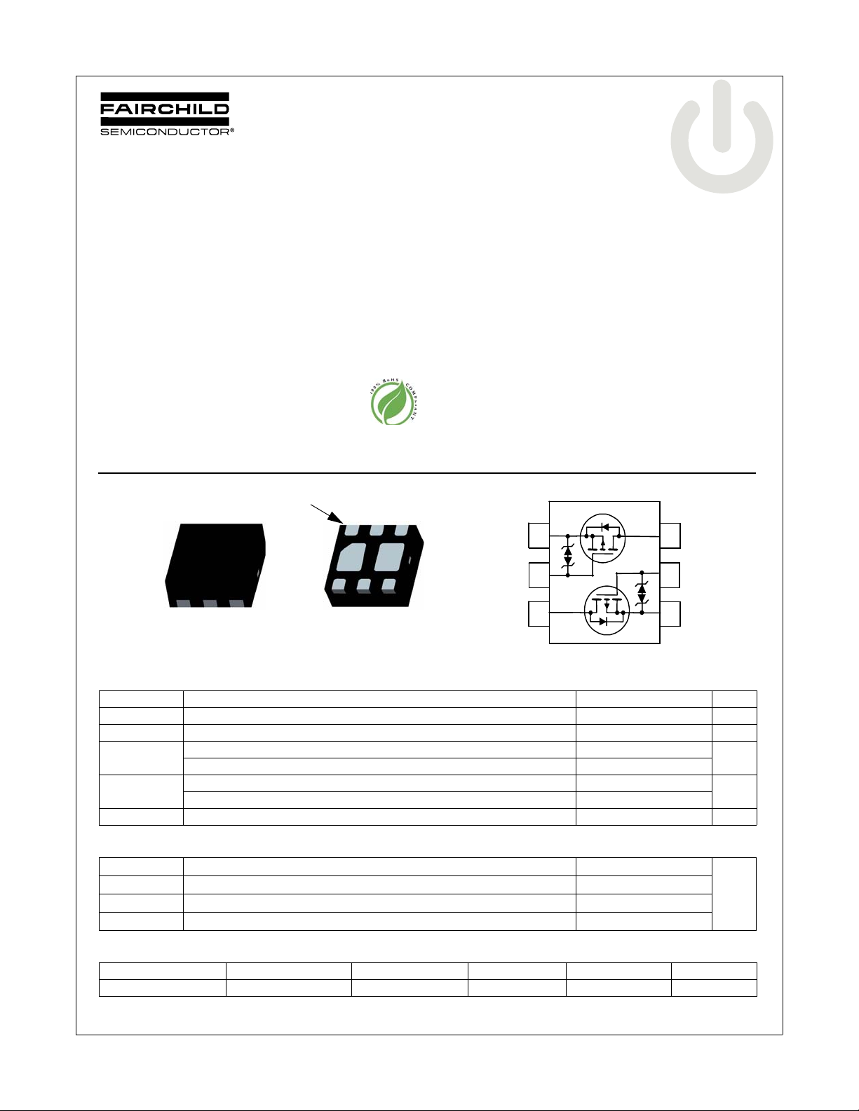
FDMA3023PZ
Dual P-Channel PowerTrench® MOSFET
-30 V, -2.9 A, 90 mΩ
Features
Max r
Max r
Max r
Max r
Low profile - 0.8 mm maximum - in the new package MicroFET
2x2 mm
HBM ESD protection level > 2 kV (Note 3)
RoHS Compliant
Free from halogenated compounds and antimony
oxides
= 90 mΩ at VGS = -4.5 V, ID = -2.9 A
DS(on)
= 130 mΩ at VGS = -2.5 V, ID = -2.6 A
DS(on)
= 170 mΩ at VGS = -1.8 V, ID = -1.7 A
DS(on)
= 240 mΩ at VGS = -1.5 V, ID = -1.0 A
DS(on)
General Description
This device is designed specifically as a single package solution
for the battery charge switch in cellular handset and other
ultra-portable applications. It features two independent
P-Channel MOSFETs with low on-state resistance for minimum
conduction losses. When connected in the typical common
source configuration, bi-directional current flow is possible.
The MicroFET 2X2 package offers exceptional thermal
performance for its physical size and is well suited to linear mode
applications.
FDMA3023PZ Dual P-Channel PowerTrench
December 2008
®
MOSFET
PIN 1
S1 G1 D2
1
S1
1
1
1
1
1
1
D1 D2
2
G1
2
2
2
2
2
2
D2
3
3
3
3
3
3
D1 G2
MicroFET 2x2
MOSFET Maximum Ratings T
Symbol Parameter Ratings Units
V
DS
V
GS
I
D
P
D
, T
T
J
STG
Drain to Source Voltage -30 V
Gate to Source Voltage ±8 V
Drain Current -Continuous (Note 1a) -2.9
-Pulsed -6
Power Dissipation (Note 1a) 1.4
Power Dissipation (Note 1b) 0.7
Operating and Storage Junction Temperature Range -55 to +150 °C
A
S2
= 25 °C unless otherwise noted
3
6
D1
6
6
6
6
6
6
G2
5
5
5
5
5
5
5
S2
4
4
4
4
4
4
4
Thermal Characteristics
R
θJA
R
θJA
R
θJA
R
θJA
Thermal Resistance for Single Operation, Junction to Ambient (Note 1a) 86
Thermal Resistance for Single Operation, Junction to Ambient (Note 1b) 173
Thermal Resistance for Dual Operation, Junction to Ambient (Note 1c) 69
Thermal Resistance for Dual Operation, Junction to Ambient (Note 1d) 151
Package Marking and Ordering Information
A
W
°C/W
Device Marking Device Package Reel Size Tape Width Quantity
323 FDMA3023PZ MicroFET 2X2 7 ’’ 8 mm 3000 units
©2008 Fairchild Semiconductor Corporation
FDMA3023PZ Rev.B1
1
www.fairchildsemi.com
Page 2
FDMA3023PZ Dual P-Channel PowerTrench
Electrical Characteristics T
= 25 °C unless otherwise noted
J
Symbol Parameter Test Conditions Min Typ Max Units
Off Characteristics
BV
∆BV
∆T
I
DSS
I
GSS
DSS
DSS
J
Drain to Source Breakdown Voltage ID = -250 µA, VGS = 0 V -30 V
Breakdown Voltage Temperature
Coefficient
Zero Gate Voltage Drain Current VDS = -24 V, V
Gate to Source Leakage Current VGS = ±8 V, V
I
= -250 µA, referenced to 25 °C -24 mV/°C
D
= 0 V -1 µA
GS
= 0 V ±100 nA
DS
On Characteristics
V
GS(th)
∆V
∆T
r
DS(on)
g
FS
GS(th)
J
Gate to Source Threshold Voltage VGS = VDS, ID = -250 µA -0.4 -0.6 -1.0 V
Gate to Source Threshold Voltage
Temperature Coefficient
Static Drain to Source On Resistance
I
= -250 µA, referenced to 25 °C 3 mV/°C
D
= -4.5 V, ID = -2.9 A 71 90
V
GS
V
= -2.5 V, ID = -2.6 A 97 130
GS
= -1.8 V, ID = -1.7 A 122 170
V
GS
= -1.5 V, ID = -1.0 A 151 240
V
GS
= -4.5 V, ID = -2.9 A, TJ = 125 °C 110 140
V
GS
Forward Transconductance VDS = -5 V, ID = -2.9 A 10 S
Dynamic Characteristics
C
iss
C
oss
C
rss
Input Capacitance
Output Capacitance 55 70 pF
Reverse Transfer Capacitance 45 65 pF
= -15 V, VGS = 0 V,
V
DS
f = 1 MHz
400 530 pF
mΩ
®
MOSFET
Switching Characteristics
t
d(on)
t
r
t
d(off)
t
f
Q
g(TOT)
Q
gs
Q
gd
Turn-On Delay Time
Rise Time 410ns
Turn-Off Delay Time 62 100 ns
Fall Time 18 33 ns
Total Gate Charge
Gate to Source Charge 0.9 nC
Gate to Drain “Miller” Charge 1.9 nC
Drain-Source Diode Characteristics
I
S
V
SD
t
rr
Q
rr
Maximum Continuous Drain-Source Diode Forward Current -1.1 A
Source to Drain Diode Forward Voltage V
Reverse Recovery Time
Reverse Recovery Charge 6.6 13 nC
510ns
= -15 V, ID = -1.0 A,
V
DD
V
= -4.5 V, R
GS
= -15 V, ID = -2.9 A
V
DD
V
= -4.5 V
GS
= 0 V, IS = -1.1 A (Note 2) -0.8 -1.2 V
GS
= -2.9 A, di/dt = 100 A/µs
I
F
GEN
= 6 Ω
7.9 11 nC
18 33 ns
©2008 Fairchild Semiconductor Corporation
FDMA3023PZ Rev.B1
2
www.fairchildsemi.com
Page 3
Notes:
1. R
is determined with the dev ice mounted on a 1 in2 oz. copper pad on a 1.5 x 1.5 in. board of FR-4 material. R
θJA
user's board design.
(a) R
(b) R
(c) R
(d) R
2. Pulse Test : Pulse Width < 300 us, Duty Cycle < 2.0%
3. The diode connected between the gate and source serves only as protection against ESD. No gate overvoltage rating is implied.
= 86 °C/W when mounted on a 1 in2 pad of 2 oz copper, 1.5 " x 1.5 " x 0.062 " thick PCB. For single operation.
θJA
= 173 °C/W when mounted on a minimum pad of 2 oz copper. For single operation.
θJA
= 69 oC/W when mounted on a 1 in2 pad of 2 oz copper, 1.5 ” x 1.5 ” x 0.062 ” thick PCB. For dual operation.
θJA
= 151 oC/W when mounted on a minimum pad of 2 oz copper. For dual operation.
θJA
o
b)173
a)86 oC/W when
mounted on a 1
2
pad of 2 oz
in
copper.
C/W when
mounted on a
minimum pad of 2
oz copper.
is guaranteed by design while R
θJC
c)69 oC/W when
mounted on a 1 in
pad of 2 oz copper.
FDMA3023PZ Dual P-Channel PowerTrench
is determined by the
θJA
o
d)151
C/W when
2
mounted on a
minimum pad of 2 oz
copper.
®
MOSFET
©2008 Fairchild Semiconductor Corporation
FDMA3023PZ Rev.B1
3
www.fairchildsemi.com
Page 4

FDMA3023PZ Dual P-Channel PowerTrench
Typical Characteristics T
6
5
4
3
2
DRAIN CURRENT (A)
,
D
-I
1
0
0 0.5 1.0 1.5 2.0
-V
,
DS
Figure 1.
On Region Characteristics Figure 2.
1.6
ID = -2.9 A
V
= -4.5 V
1.4
GS
1.2
1.0
NORMALIZED
0.8
DRAIN TO SOURCE ON-RESISTANCE
0.6
-75 -50 -25 0 25 50 75 100 125 150
T
,
JUNCTION TEMPERATURE
J
VGS = -3.5 V
VGS = -2.5 V
VGS = -1.8 V
PULSE DURATION = 80 µs
DUTY CYCLE = 0.5% MAX
DRAIN TO SOURCE VOLTAGE (V)
= 25 °C unless otherwise noted
J
VGS = -4.5 V
VGS = -1.5 V
o
(
C
)
NORMALIZED
6
5
4
3
2
PULSE DUR ATION = 80 µs
DUTY CYCLE = 0.5% MAX
V
= -1.5 V
GS
VGS = -2.5 V
V
GS
= -1.8 V
1
DRAIN TO SOURCE ON-RESISTANCE
0
123456
VGS = -3.5 V
-I
,
DRAIN CURRENT (A)
D
VGS = -4.5 V
Normali z e d O n - R esistance
vs Drain Current and Gate Voltage
400
)
Ω
m
(
300
200
DRAIN TO
,
DS(on)
r
100
SOURCE ON-RESISTANCE
0
1.0 1.5 2.0 2.5 3.0 3.5 4.0 4.5
-V
,
GATE TO SOURCE VOL TA G E (V)
GS
PULSE DURATION = 80 µs
DUTY CYCLE = 0.5% MAX
ID = -1.45 A
TJ = 125 oC
TJ = 25 oC
®
MOSFET
Fig u re 3. Norma l ized O n Res i stan c e
vs Junction Temperature
6
PULSE DURATION = 80 µs
DUTY CYCLE = 0.5% MAX
5
V
= -5 V
DS
4
3
TJ = 125 oC
2
, DRAIN CURRENT (A)
D
-I
1
0
0.5 1.0 1.5 2.0
TJ = 25 oC
-VGS, GATE TO SOURCE VOLTAGE (V)
Figure 5. Transfer Characteristics
©2008 Fairchild Semiconductor Corporation
FDMA3023PZ Rev.B1
TJ = -55 oC
Figure 4.
On-R esistance vs Gate to
Source Voltage
10
V
= 0 V
GS
1
TJ = 125 oC
0.1
TJ = 25 oC
0.01
, REVERSE DRAIN CURRENT (A)
S
-I
0.001
0.2 0.4 0.6 0.8 1.0 1.2
-VSD, BODY DIODE FORWARD VOLTAGE (V)
Figure 6.
TJ = -55 oC
Source to Drain Di ode
Forward Voltage vs Source Current
4
www.fairchildsemi.com
Page 5

FDMA3023PZ Dual P-Channel PowerTrench
Typical Characteristics T
5
ID = -2.9 A
4
VDD = -10 V
3
2
1
, GATE TO SOURCE VOLTAGE (V)
GS
-V
0
0246810
Qg, GATE CHARGE (nC)
Figure 7.
-2
10
-3
10
-4
10
-5
10
-6
10
-7
10
-8
10
, GATE LEAKAGE CURRENT (A)
g
-I
-9
10
Figure 9.
03691215
Gate Charge Characteristics Figure 8.
V
= 0 V
GS
TJ = 125 oC
,
-V
GATE TO SOURCE VOLTAGE (V)
GS
Gate Leakage vs Gate to Source Voltage Figure 10.
= 25 °C unless otherwise noted
J
VDD = -15 V
V
= -20 V
DD
TJ = 25 oC
1000
100
CAPACITANCE (pF)
f = 1 MHz
V
= 0 V
GS
10
0.1 1 10 30
-VDS, DRAIN TO SOURCE VOLTAGE (V)
Capacitance vs Drain
to Source Voltage
10
THIS AREA IS
LIMITED BY r
DS(on)
1
0.1
, DRAIN CURRENT (A)
D
-I
0.01
0.01 0.1 1 10 100
SINGLE PULSE
= MAX RATED
T
J
R
= 173 oC/W
θ
JA
= 25 oC
T
A
-VDS, DRAIN to SOURCE VOLTAGE (V)
Forward Bias Safe Operating Area
C
C
C
1 ms
10 ms
100 ms
1 s
10 s
DC
iss
oss
rss
®
MOSFET
200
200
VGS = -4.5 V
100
10
PEAK TRANSIENT POWER (W)
,
)
PK
1
(
P
0.5
-3
10
©2008 Fairchild Semiconductor Corporation
FDMA3023PZ Rev.B1
-2
10
-1
10
t, PULSE WIDTH (sec)
110
Figure 11. Single Pulse Maximum Power Dissipation
5
SINGLE PULSE
= 173 oC/W
R
θ
JA
= 25 oC
T
A
www.fairchildsemi.com
1000
Page 6

FDMA3023PZ Dual P-Channel PowerTrench
Typical Characteristics T
NORMALIZED THERMAL
JA
θ
Z
0.1
IMPEDANCE,
0.01
0.005
2
1
DUTY CYCLE-DESCENDING ORDER
D = 0.5
0.2
0.1
0.05
0.02
0.01
-3
10
10
Figure 12.
SINGLE PULSE
R
-2
= 25 °C unless otherwise noted
J
NOTES:
DUTY FACTOR: D = t
= 173 oC/W
θ
JA
-1
10
t, RECTANGULAR PULSE DURATION (sec)
110
PEAK TJ = PDM x Z
Junction-to-Ambient Transient Thermal Response Curve
P
DM
t
1
t
2
1/t2
x R
+ T
θJA
θJA
A
100 1000
®
MOSFET
©2008 Fairchild Semiconductor Corporation
FDMA3023PZ Rev.B1
6
www.fairchildsemi.com
Page 7

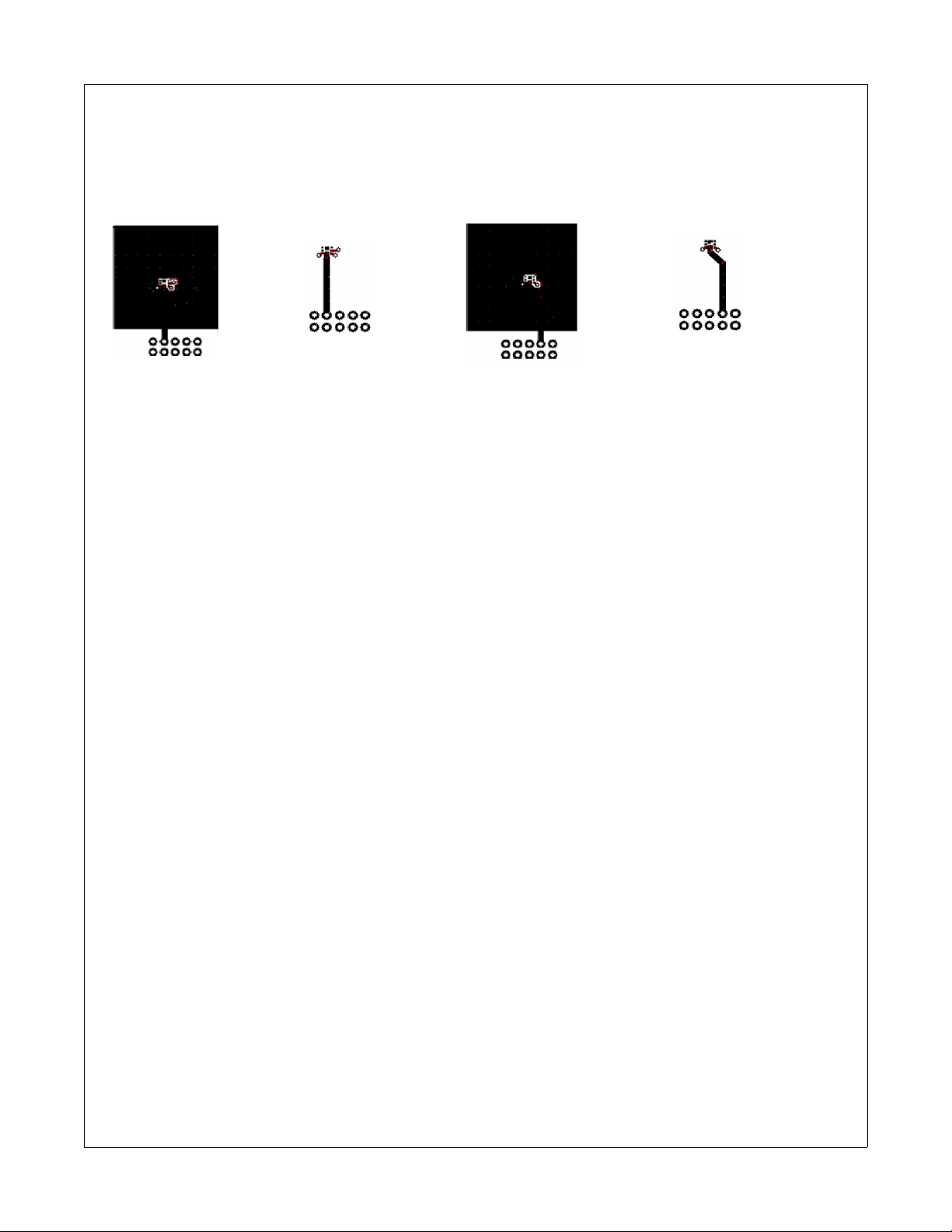
Dimensional Outline and Pad Layout
FDMA3023PZ Dual P-Channel PowerTrench
2X
PIN#1 QUADRANT
0.8 MAX
PIN#1 IDENT
D
0.05
0.00
0.20
0.35
0.65
2.0
TOP VIEW
SIDE VIEW
1.64? .10
0.35? .10
1.30
BOTTOM VIEW
A
2.0
2X
(0.18 5 )
(0.6 5)
0.25~0.35
B
(0.20)
C
0.86? .10
(1.80 )
(0.80 )
(1.00)
(0.4 2)
0.65
(0.10)
(0.5 0)
(2.2 5)
(0.42 )
RECOMMENDED LAND PATTERN
®
MOSFET
A. CONFORMS TO JEDEC REGISTRATION MO-229,
VARIATION VCCC EXC EPT AS NOTED.
B . D IME NSION S AR E IN M IL L IME T E RS .
C. DIMENSIONS AND TOLERANCES PER
ASM E Y 14.5M, 1994
D. NON-JEDEC DUAL DAP
MLP 06JrevB
©2008 Fairchild Semiconductor Corporation
FDMA3023PZ Rev.B1
7
www.fairchildsemi.com
Page 8

TRADEMARKS
tm
®
tm
tm
The following includes registered and unregistered tra demarks and service marks, owned by Fairchild Semico nductor and/or its glo bal subsidiaries, and is not
intended to be an exhaustive list of all such trademarks.
Build it Now™
CorePLUS™
CorePOWER™
CROSSVOLT™
CTL™
Current Transfer Logic™
EcoSPARK
EfficentMax™
EZSWITCH™ *
™
Fairchild
Fairchild Semiconductor
FACT Quiet Series™
FACT
FAST
FastvCore™
FlashWriter
FPS™
F-PFS™
* EZSWITCH™ and FlashWriter
DISCLAIMER
FAIRCHILD SEMICONDUCTOR RESERVES THE RIGHT TO MAKE CHANGES WITHOUT FURTHER NOTICE TO ANY PRODUCTS HEREIN TO IMPROVE
RELIABILITY, FUNCTION, OR DESIGN. FAIRCHILD DOES NOT ASSUME ANY LIABILITY ARISING OUT OF THE APPLICATION OR USE OF ANY
PRODUCT OR CIRCUIT DESCRIBED HEREIN; NEITHER DOES IT CONVEY ANY LICENSE UNDER ITS PATENT RIGHTS, NOR THE RIGHTS OF OTHERS.
THESE SPECIFICATIONS DO NOT EXPAND THE TERMS OF FAIRCHILD’S WORLDWIDE TERMS AND CONDITIONS, SPECIFICALLY THE WARRANTY
THEREIN, WHICH COVERS THESE PRODUCTS.
®
®
®
®
®
*
®
®
are trademarks of System General Corporation, used under license by Fairchild Semiconductor.
®
FRFET
Global Power Resource
Green FPS™
Green FPS™ e-Series™
GTO™
IntelliMAX™
ISOPLANAR™
MegaBuck™
MICROCOUPLER™
MicroFET™
MicroPak™
MillerDrive™
MotionMax™
Motion-SPM™
OPTOLOGIC
OPTOPLANAR
PDP SPM™
Power-SPM™
PowerTrench
®
®
®
®
PowerXS™
SM
Programmable Active Droop™
®
QFET
QS™
Quiet Series™
RapidConfigure™
™
Saving our world, 1mW /W /kW at a time™
SmartMax™
SMART START™
®
SPM
STEALTH™
SuperFET™
SuperSOT™-3
SuperSOT™-6
SuperSOT™-8
SupreMOS™
SyncFET™
®
The Power Franchise
®
TinyBoost™
TinyBuck™
®
TinyLogic
TINYOPTO™
TinyPower™
TinyPWM™
TinyWire™
µSerDes™
®
UHC
Ultra FRFET™
UniFET™
VCX™
VisualMax™
XS™
FDMA3023PZ Dual P-Channel PowerTrench
®
MOSFET
LIFE SUPPORT POLICY
FAIRCHILD’S PRODUCTS ARE NOT AUTHORIZED FOR USE AS CRITICAL COMPONENTS IN LIFE SUPPORT DEVICES OR SYSTEMS WITHOUT THE
EXPRESS WRITTEN APPROVAL OF FAIRCHILD SEMICONDUCTOR CORPORATION.
As used herein:
1. Life support devices or systems are devices or systems which, (a) are
intended for surgical implant into the body or (b) support or sustain life,
and (c) whose failure to perform when properly used in accordance with
instructions for use provided in the labeling, can be reasonably
2. A critical component in any component of a life support, device, or
system whose failure to perform can be reasonably expected to cause
the failure of the life support device or system, or to affect its safety or
effectiveness.
expected to result in a significant injury of the user.
ANTI-COUNTERFEITING POLICY
Fairchild Semiconductor Corporation’s Anti-Counterfeiting Policy. Farichild’s Anti-Counterfeiting Policy is also stated on our external website,
www.fairchildsemi.com, under Sales Support
Counterfeiting of semiconductor parts is a growing prob lem in the indust ry. All manufactur es of semiconductor product s are experiencin g counterfeiting of their
parts. Customers who inadvertently purchase count erfeit par ts experience many problems such as loss of brand reputation, substandard performance, failed
application, and increased cost of production and man ufacturing delays. Fairchild is taking strong measures to protect ourselve s and our customers from the
proliferation of counterfeit parts. Farichild stro ngly encourage s customers t o purchase Farichild par ts either dire ctly from Fairchil d or from Authorized Fa irchild
Distributors who are listed by country on our web page cited above. Products customers buy either from fairchild directly or from Authorized Fairchild
Distributors are genuine parts, have full traceability, meet Fairchild’s quality standards for handing and storage and provide access to Farichild’s full range of
up-to-date technical and product information. Fairchild and our Authorized Distributors will stand behind all warranties and will appropriately address and
warranty issues that may arise. Fairchild will not provide any warranty coverage or other assistance for parts bought from Unauthorized Sources. Farichild is
committed to combat this global problem and encourage our customers t o do their part in st opping this practice by buying direct or from authorized distrib utors.
PRODUCT STATUS DEFINITIONS
Definition of Terms
.
Datasheet Identification Product Status Definition
Advance Information Formative / In Design
Preliminary First Production
No Identification Needed Full Production
Obsolete Not In Production
Datasheet contains the design specifications f or product development. S pecifications may
change in any manner without notice.
Datasheet contains preliminary data; sup plementary dat a will be pu blished at a lat er date.
Fairchild Semiconductor reserves the right to make ch anges at any time without notice to
improve design.
Datasheet contains final specifications. Fairchild Semiconductor reserves the right to
make changes at any time without notice to improve the design.
Datasheet contains specifications on a product that is discontinued by Fairchild
Semiconductor. The datasheet is for reference information only.
Rev. I37
©2008 Fairchild Semiconductor Corporation 8 www.fairchildsemi.com
FDMA3023PZ Rev.B1
 Loading...