

Page 1
Ordering number : ENN7021
FC21
TR : NPN Epitaxial Planar Silicon Transistor
FET : N-Channel Silicon Junction FET
FC21
High-Frequency Amplifier ,
AM tuner RF Amplifier Applications
Features
•
The FC21 contains both a 2SK1740 equivalent chip
and a 2SC2812 equivalent chip in the CP package,
thus realizes higher efficiency in device mounting
on the PCB.
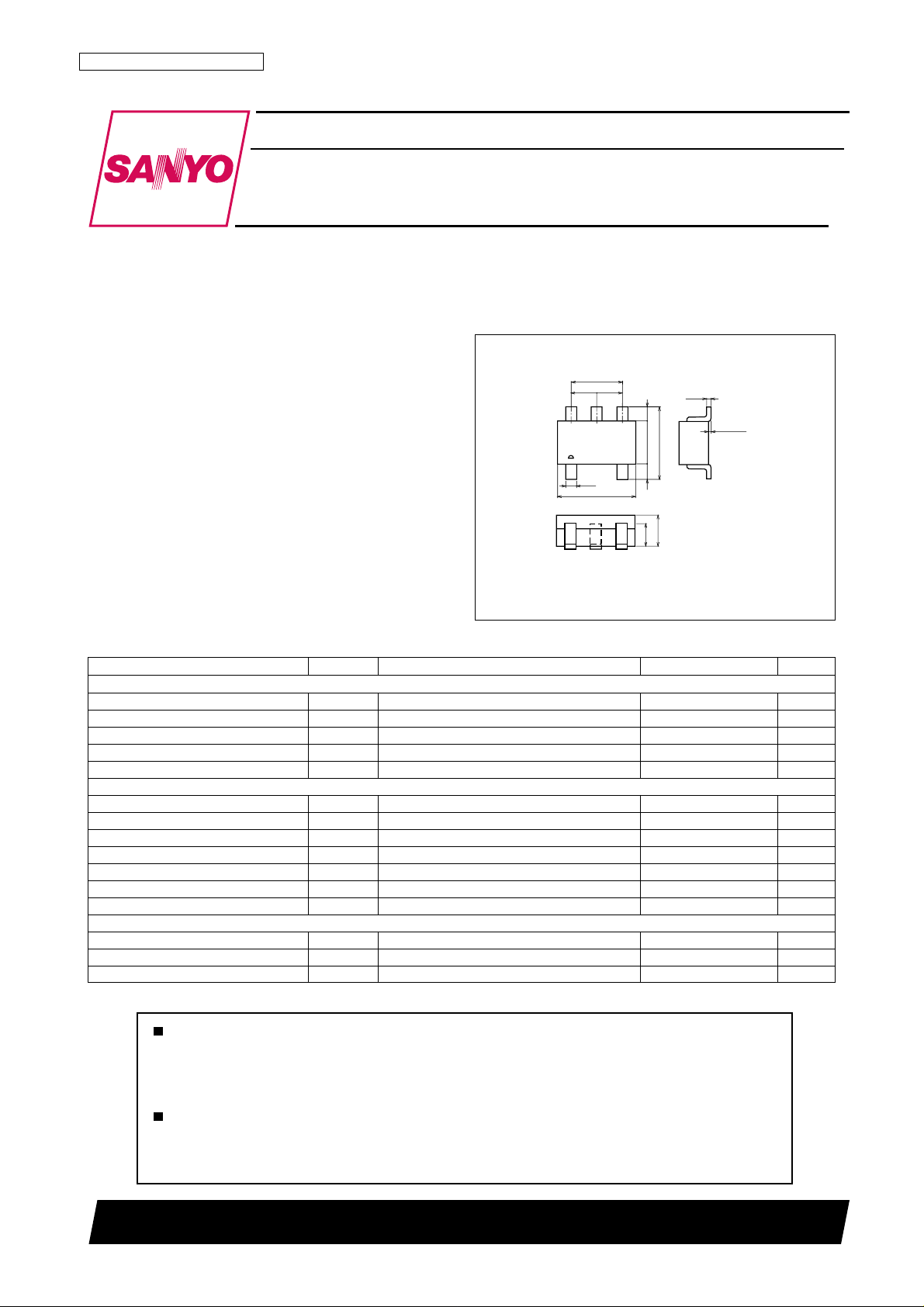
Package Dimensions
unit : mm
2122
[FC21]
1.9
0.95 0.95
54
1
0.4
2.9
3
0.60.6
1.6
2
0.8
0.16
2.8
1 : Collector
2 : Gate
3 : Source
1.1
4 : Emitter/Drain
5 : Base
SANYO : CP5
0 to 0.1
Specifications
Absolute Maximum Ratings at Ta=25°C
Parameter Symbol Conditions Ratings Unit
[FET]
Drain-to-Source Voltage V
Gate-to-Drain Voltage V
Gate Current I
Drain Current I
Allowable Power Dissipation P
[TR]
Collector-to-Base Voltage V
Collector-to-Emitter Voltage V
Emitter-to-Base Voltage V
Collector Current I
Collector Current(Pulse) I
Base Current I
Collector Dissipation P
[Common Ratings]
Total Dissipation P
Junction T emperature Tj 150 °C
Storage T emperature T stg --55 to +150 °C
Marking : 1C
DSX
GDS
G
D
D
CBO
CEO
EBO
C
CP
B
C
T
40 V
--40 V
10 mA
75 mA
400 mW
55 V
50 V
6V
150 mA
300 mA
30 mA
200 mW
600 mW
Any and all SANYO products described or contained herein do not have specifications that can handle
applications that require extremely high levels of reliability, such as life-support systems, aircraft's
control systems, or other applications whose failure can be reasonably expected to result in serious
physical and/or material damage. Consult with your SANYO representative nearest you before using
any SANYO products described or contained herein in such applications.
SANYO assumes no responsibility for equipment failures that result from using products at values that
exceed, even momentarily, rated values (such as maximum ratings, operating condition ranges, or other
parameters) listed in products specifications of any and all SANYO products described or contained
herein.
SANYO Electric Co.,Ltd. Semiconductor Company
TOKYO OFFICE Tokyo Bldg., 1-10, 1 Chome, Ueno, Taito-ku, TOKYO, 110-8534 JAPAN
81001 TS IM TA-1526
No.7021-1/5
Page 2
FC21
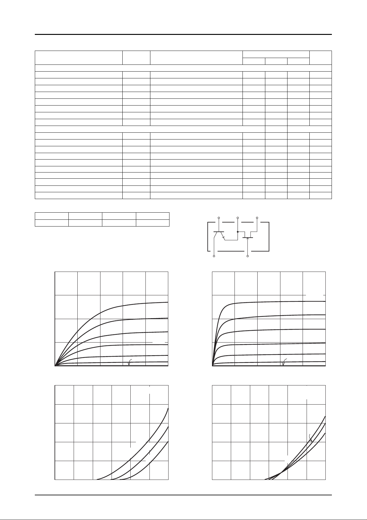
B S
CG
E / D
Electrical Characteristics at Ta=25°C
Parameter Symbol Conditions
[FET]
Gate-to-Drain Breakdown Voltage V
Gate Cutoff Current I
Cutoff Voltage VGS(off) VDS=10V , ID=100µA --2.0 --3.0 --5.0 V
Drain Current I
Forward Transfer Admittance
Input Capacitance Ciss VDS=10V, VGS=0, f=1MHz 11 pF
Reverse Transfer Capacitance Crss VDS=10V, VGS=0, f=1MHz 2.5 pF
Noise Figure NF VDS=10V, Rg=1kΩ, ID=1mA, f=1kHz 1.5 dB
[TR]
Collector Cutoff Current I
Emitter Cutoff Current I
DC Current Gain h
Gain-Bandwidth Product f
Output Capacitance Cob VCB=6V, f=1MHz 3 pF
Collector-to-Emitter Saturation Voltage VCE(sat) IC=50mA, IB=5mA 0.1 0.5 V
Base-to-Emitter Saturation Voltage VBE(sat) IC=50mA, IB=5mA 0.8 1.0 V
Collector-to-Base Breakdown Voltage V
Collector-to-Emitter Breakdown Voltage V
Emitter-to-Base Breakdown Voltage V
(BR)GDSIG
GSS
DSS
yfs
CBO
EBO
FE
T
(BR)CBOIC
(BR)CEOIC
(BR)EBOIE
=--10µA, VDS=0 --40 V
VGS=--20V, VDS=0 --1.0 nA
VDS=10V , VGS=0 40* 75* mA
VDS=10V, VGS=0, f=1kHz 22 30 mS
VCB=35V, IE=0 0.1 µA
VEB=4V, IC=0 0.1 µA
VCE=6V, IC=1mA 135 600
VCE=6V, IC=10mA 100 MHz
=10µA, IE=0 55 V
=1mA, RBE=∞ 50 V
=10µA, IC=0 6 V
Ratings
min typ max
Unit
* : The FC21 is classified by I
Rank JKL
I
DSS
The specifications shown above are for each individual FET or transistor.
80
60
40 to 52 48 to 63 57 to 75
-- mA
D
40
as follows : (unit : mA)
DSS
I
-- V
D
DS
V
GS
--0.5V
[FET]
=0
--1.0V
20
Drain Current, I
--1.5V
--2.0V
0
012345
Drain-to-Source V oltage, V
I
-- V
D
--3.0V
DS
GS
--2.5V
-- V
ITR01960 ITR01961
[FET]
VDS=10V
100
80
Electrical Connection
I
-- V
I
D
D
-- V
80
60
-- mA
D
40
20
Drain Current, I
0
048 2012 16
Drain-to-Source V oltage, V
DS
GS
--3.0V
DS
V
-- V
VDS=10V
I
=60mA
DSS
[FET]
GS
--0.5V
--1.0V
--1.5V
--2.0V
--2.5V
[FET]
=0
100
80
--6 --4--5 --3 --2 --1 0
Gate-to-Source V oltage, V
DSS
I
GS
=75mA
55mA
-- V
40mA
ITR01963
-- mA
60
D
40
Drain Current, I
20
0
25°C
75°C
Ta= --25°C
--6 --5 --4 --3 --2 --1 0
Gate-to-Source V oltage, V
GS
-- V
ITR01964
No.7021-2/5
-- mA
60
D
40
Drain Current, I
20
0
Page 3

FC21
VGS(off) -- I
-- V
(off)
GS
6
5
4
3
2
Cutoff V oltage, V
--1.0
Drain Current, I
5
3
2
10
7
Forward Transfer Admittance, yfs -- mS
5
354
yfs -- I
y
y
Drain Current, I
Ciss -- V
-- pF
7
5
3
2
fs2(V
fs
1(I
DSS
DSS
GS
=10mA)
D
DSS
DSS
=0)
DS
7543
-- mA
7
-- mA
RDS(on) -- I
DSS
VDS=10V
I
=100µA
DSS
[FET]
6
5
4
(on) -- Ω
3
DS
2
Static Drain-to-Source
On-State Resistance, R
10
100
ITR01965
[FET]
VDS=10V
f=1kHz
100
ITR01967
[FET] [FET]
VGS=0
345 7
100
7
5
3
2
10
7
5
3
Forward Transfer Admittance, yfs -- mS
2
23 57
2
Drain Current, I
yfs -- I
=40mA
I
DSS
23 57
10
Drain Current, I
Crss -- V
DSS
D
DS
-- mA
D
55mA
-- mA
f=1MHz
-- pF
10
7
5
[FET]
ID=10mA
VGS=0
ITR01966
[FET]
VDS=10V
f=1kHz
75mA
100
ITR01968
VGS=0
f=1MHz
100
2
10
7
5
Input Capacitance, Ciss
3
2
1.0
23
10
Drain-to-Source V oltage, V
P
-- Ta
D
-- mW
500
400
D
300
200
100
Allowable Power Dissipation, P
0
0 20 40 60 80 100 160120 140
Ambient Temperature, Ta -- °C
DS
-- V
ITR01981
[FET]
ITR01983
3
2
1.0
7
Reverse Transfer Capacitance, Crss
52357
5
1.0
23 57
Drain-to-Source V oltage, V
10
23 5
-- V
DS
ITR01982
No.7021-3/5
Page 4

20
50µA
16
-- mA
C
12
8
Collector Current, I
4
0
020 50403010
Collector-to-Emitter Voltage, V
3
2
1000
FE
7
5
45µA
40µA
I
C
35µA
hFE -- I
Ta=75°C
-- V
30µA
CE
25µA
C
20µA
15µA
10µA
CE
FC21
I
[TR] [TR]
IB=0
5µA
-- V
IT03592 IT03593
VCE=6V
240
200
-- mA
160
C
120
80
Collector Current, I
40
0
0 0.2 0.4 0.6 0.8 1.0 1.2
Base-to-Emitter V oltage, V
1000
7
5
-- MHz
3
T
2
-- V
C
BE
25°C
Ta=75°C
f
-- I
T
C
--25°C
BE
VCE=6V
-- V
[TR][TR]
VCE=6V
3
2
DC Current Gain, h
100
7
5
325
0.1
2
10
7
5
3
2
1.0
7
5
Output Capacitance, Cob -- pF
3
2
1.0
250
--25°C
25°C
32325
1.0
10
Collector Current, IC -- mA
Cob -- V
Collector-to-Base Voltage, V
P
CB
573257
10 100
-- Ta
C
CB
100
7
5
Gain-Bandwidth Product, f
3
100
325
2
1.0
573232
10 100
Collector Current, IC -- mA
[TR] [TR]
f=1MHz
5732
-- V
IT03596
3
2
1.0
7
5
(sat) -- V
CE
3
2
0.1
7
5
3
Collector-to-Emitter
Saturation V oltage, V
2
0.01
VCE(sat) -- I
5732
101.0
Collector Current, IC -- mA
[TR]
5732
IT03595IT03594
C
IC / IB=10
573232
100
IT03597
200
-- W
C
150
100
50
Collector Dissipation, P
0
2006040 80 100 140120 160
Ambient Temperature, Ta -- °C
ITR10349
No.7021-4/5
Page 5

FC21
Specifications of any and all SANYO products described or contained herein stipulate the performance,
characteristics, and functions of the described products in the independent state, and are not guarantees
of the performance, characteristics, and functions of the described products as mounted in the customer's
products or equipment. To verify symptoms and states that cannot be evaluated in an independent device,
the customer should always evaluate and test devices mounted in the customer's products or equipment.
SANYO Electric Co., Ltd. strives to supply high-quality high-reliability products. However, any and all
semiconductor products fail with some probability. It is possible that these probabilistic failures could
give rise to accidents or events that could endanger human lives, that could give rise to smoke or fire,
or that could cause damage to other property. When designing equipment, adopt safety measures so
that these kinds of accidents or events cannot occur. Such measures include but are not limited to protective
circuits and error prevention circuits for safe design, redundant design, and structural design.
In the event that any or all SANYO products(including technical data,services) described or
contained herein are controlled under any of applicable local export control laws and regulations,
such products must not be exported without obtaining the export license from the authorities
concerned in accordance with the above law.
No part of this publication may be reproduced or transmitted in any form or by any means, electronic or
mechanical, including photocopying and recording, or any information storage or retrieval system,
or otherwise, without the prior written permission of SANYO Electric Co. , Ltd.
Any and all information described or contained herein are subject to change without notice due to
product/technology improvement, etc. When designing equipment, refer to the "Delivery Specification"
for the SANYO product that you intend to use.
Information (including circuit diagrams and circuit parameters) herein is for example only ; it is not
guaranteed for volume production. SANYO believes information herein is accurate and reliable, but
no guarantees are made or implied regarding its use or any infringements of intellectual property rights
or other rights of third parties.
This catalog provides information as of August, 2001. Specifications and information herein are subject
to change without notice.
No.7021-5/5
PS
 Loading...