

Page 1

FAN8725 (KA3025)
Spindle Motor and 5-Channel Motor Driver
www.fairchildsemi.com
Features
Common
• Built-in thermal shutdown circuit (TSD)
• Built-in power save circuit
• 3 Independent voltage source
• Corresponds to 3.3V or 5V DSP
Spindle
• Built-in hall bias
• Built-in FG signal output circuit
• Built-in rotational direction detecting circuit
• Built-in protection circuit for reverse rotation
• Built-in short brake circuit
BTL (5-channel)
• Built-in 5-CH balanced transformerless (BTL) driver
• Built-in Level shift circuit
• Independent voltage sources
• VM2 = CH1,CH2 / VM3 = CH3, CH4 ,CH5
Description
The FAN8725 is a monolithic IC suitable for a 3-phase
BLDC spindle motor driver and 5-ch motor drivers which
drives the focus actuator, tracking actuator, loading motor,
stepping motor driver of the CD-media systems.
48-QFPH-1414
Typical Applications
• Compact disk R OM (CD-ROM)
• Compact disk RW (CD-RW)
• Digital video disk ROM (DVD-ROM)
• Digital video disk RAM (DVD-RAM)
• Digital video disk Player (DVDP)
• Other compact disk media
©2000 Fairchild Semiconductor International
Ordering Information
Device Package Operating Temp.
FAN8725 48-QFPH-1414 −35°C ~ +85°C
Rev. 1.0.1
March. 2000.
1
Page 2

FAN8725 (KA3025)
Pin Assignments
VH
48 47 46 45 44 43 42 41 40 39 38 37
PC1
EC
ECR
PS
SB
VREF
SVCC2
VM3
OUT5
IN5
PGND3
H1+
H1-
H2+
H2-
H3+
H3-
FG
DIR
SVCC1
VM1
CS1
PGND1
1
2
3
4
5
6
DO5 -
36
35
DO5+
DO4 -
34
DO4+
32
DO3 -
32
DO3+
31
FAN8725
7
8
9
10
11
12
30
PGND2
DO2 -
29
DO2+
28
DO1 -
27
26
DO1+
OUT1
25
13 14 15 16 17 18 19 20 21 22 23 24
A2
A3
A1
SGND2
OUT4
IN4
OUT3
IN3
IN2
OUT2
VM2
2
IN1
Page 3

Pin Definitions
Pin Number Pin Name I/O Pin Function Description
1 H1- I Hall 1(-) input
2 H1+ I Hall 1(+) input
3 H2+ I Hall 2(-) input
4 H2- I Hall 2(+) input
5 H3+ I Hall 3(-) input
6 H3- I Hall 3(+) input
7 FG O Frequency Generator output
8 DIR O Rotation direction output
9 SVCC1 - Spindle Signal supply voltage
10 VM1 - Spindle power supply
11 CS1 I Spindle current sense
12 PGND1 - Spindle power ground
13 A1 O 3-phase output1
14 A2 O 3-phase output2
15 A3 O 3-phase output3
16 SGND2 - CH signal ground
17 IN4 I OP-Amp CH 4 input(-)
18 OUT4 O OP-Amp CH 4 output
19 IN3 I OP-Amp CH 3 input(-)
20 OUT3 O OP-Amp CH 3 output
21 IN2 I OP-Amp CH 2 input(-)
22 OUT2 O OP-Amp CH 2 output
23 VM2 - CH1/CH2 power supply
24 IN1 I OP-Amp CH 1 input(-)
25 OUT1 O OP-Amp CH 1 output
26 DO1+ O Channel 1 output (+)
27 DO1 - O Channel 1 output (−)
28 DO2+ O Channel 2 output (+)
29 DO2 - O Channel 2 output (−)
30 PGND2 - CH1/CH2 power ground
31 DO3+ O Channel 3 output (+)
32 DO3 - O Channel 3 output (−)
33 DO4+ O Channel 4 output (+)
FAN8725 (KA3025)
3
Page 4

FAN8725 (KA3025)
Pin Definitions (Continued)
Pin Number Pin Name I/O Pin Function Description
34 DO4 - O Channel 4 output (−)
35 DO5+ O Channel 5 output (+)
36 DO5- O Channel 5 output (−)
37 PGND3 - CH3/CH4/CH5 power ground
38 IN5 I OP-Amp CH 5 input(-)
39 OUT5 O OP-Amp CH 5 output
40 VM3 - CH3/CH4/CH5 power supply
41 SVCC2 - CH Signal supply voltage
42 VREF I BTL reference voltage
43 SB I Short brake
44 PS I Power save
45 ECR I Torque control reference
46 EC I Torque control
47 PC1 - Phase compensation capacitor
48 VH I Hall bias
Notes:
BTL drive part symbol(+,- outputs of drives) is determined according to the polarity of input pin.
(For example, if the voltage of pin 24 is high, the output of pin 26 is high)
4
Page 5

Internal Block Diagram
FAN8725 (KA3025)
H1+
H1 -
H2+
H2 -
H3+
H3 -
FIN(GND)
FG
DIR
PC1
EC
CS1VM
ECR
454647
Absolute Values
Output
Current Limit
VH
48
Hall
1
2
3
4
5
Bias
Hall Amp
SB
PS
4344 42 41 40 39 38 37
Current
Sense Amp
FIN(GND)
VREF
SVCC2
VM3
OUT5
CH5
X8
CH4
X8
IN5
PGND3
36
35
34
33
32
DO5 -
DO5+
DO4 -
DO4+
DO3 -
CH3
6
Detection
FG
Generator
7
8
Logic
Reverse
Rotation
Short
Brake
VM3
VM2
R
R
VM3
R
R
VM2
X8
CH2
X5
VM3
VM2
31
30
29
DO3+
FIN(GND)
PGND2
DO2 -
SVCC1
VM1
CS1
PGND1
10
11
12
9
Distributor
Driver
13 16
14 18
A1
A2
15
A3
17
IN4
SGND2
OUT4
FIN(GND)
5
19 20
IN3
21
OUT3
IN2
CH1
X5
22 23
OUT2
VM2
24
IN1
28
27
26
25
DO2+
DO1 -
DO1+
OUT1
Page 6
FAN8725 (KA3025)
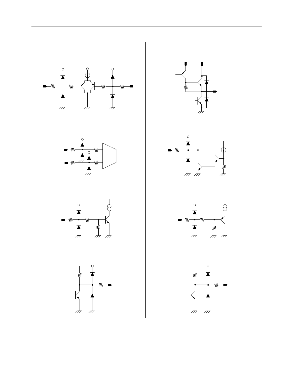
Equivalent Circuits (Spindle Part)
HALL INPUT DRIVER OUTPUT
Pin
10
Pin
11
Pin
1,3,5
22.5Ω
1KΩ 1KΩ
22.5Ω
Pin
2,4,6
15KΩ
TORQUE CONTROL INPUT HALL BIAS INPUT
Pin 45
22.5Ω
22.5Ω
Pin 46
1KΩ
1KΩ
+
Pin 48
5Ω
-
POWER SAVE INPUT SHORT BRAKE INPUT
Pin 44
22.5Ω
40KΩ
30KΩ
Pin 43
22.5Ω
1KΩ
Pin 13,14,15
100KΩ
20KΩ
FG OUTPUT DIR OUTPUT
10KΩ
Vcc
22.5Ω
Pin
7
Vcc
30KΩ
6
22.5Ω
Pin 8
Page 7

Equivalent Circuits (BTL Part)
OP-AMP INPUT OP-AMP OUTPUT
FAN8725 (KA3025)
Pin
24,21,
19,17,38
40kΩ
20kΩ
22.5Ω
20KΩ
1KΩ
20KΩ
DRIVE OUTPUT VREF
CH-O
20kΩ
(Pin 26,28,31,33,35 )
CH-O
(Pin 27,29,32,34,36)
Pin 42
22.5Ω
20KΩ
1KΩ
Pin
25,22,20,18,39
20KΩ
7
Page 8

FAN8725 (KA3025)
Absolute Maximum Ratings (Ta = 25°°°°C)
Parameter Symbol Value Unit
Supply Voltage (Spindle Signal) SV
Supply Voltage (BTL Signal) SV
Supply Voltage (Spindle Motor) V
Supply Voltage (BTL CH1/2) V
Supply Voltage (BTL CH3/4/5) V
Power dissipation P
Operating Temperature Range T
Storage temperature Range T
Maximum Output Current (Spindle) I
Maximum Output Current (BTL) I
NOTE:
1. When mounted on 70mm × 70mm × 1.6mm PCB (Phenolic resin materi al)
2. Power dissipation is reduced 24mW/°C for using above Ta=25°C
3. Do not exceed P
and SOA (Safe Operating Area)
D
CC1max
CC2max
M1max
M2max
M3max
D
OPR
STG
Omaxa
Omaxb
Power Dissipation Curve
7V
15 V
15 V
15 V
15 V
note
3.0
W
-35 ~ +85 °C
-55 ~ +150 °C
1.3 A
0.6 A
Pd [mW]
3,000
2,000
1,000
0
0 85
Recommended Operating Conditions (Ta = 25°°°°C)
Parameter Symbol Min. Typ. Max. Unit
Operating Supply Voltage (Spindle Signal) SV
Operating Supply Voltage (BTL Signal) SV
Operating Supply Voltage (Spindle Motor) V
Operating Supply Voltage (BTL CH1/2) V
Operating Supply Voltage (BTL CH3/4/5) V
CC1
CC2
M1
M2
M3
1751501251005025
Ambient Temperature, Ta [°C]
4.5 – 5.5 V
10.8 – 13.2 V
10.8 – 13.2 V
4.5 – SV
4.5 – SV
CC2
CC2
V
V
8
Page 9

Electrical Characteristics (Ta = 25°°°°C)
Parameter Symbol Condition Min. Typ. Max. Units
FULL CHIP
Quiescent Circuit Current 1 I
Quiescent Circuit Current 2 I
Quiescent Circuit Current 3 I
CC1
CC2
CC3
POWER SAVE
On Voltage Range V
Off Voltage Range V
PSon
PSoff
HALL BIAS
Hall Bias Voltage V
HB
HALL AMP
Hall Bias Current I
Common Mode Input Range V
Minimum in Level V
H1 Hysteresis V
HA
HAR
INH
HYS
TORQUE CONTROL
Ecr In Voltage Range E
Ec In Voltage Range E
Offset Voltage (-) E
Offset Voltage (+) E
In Current E
E
C
E
In Current E
CR
In/output Gain G
CR
C
Coff-
Coff+
Cin
CRin
EC
FG
FG Output Voltage (H) V
FG Output Voltage (L) V
FGh
FHl
Duty(Reference Value) R
OUTPUT BLOCK
Saturation Voltage (upper TR) V
Saturation Voltage (lower TR) V
Torque Limit Current I
Oh
Ol
TL
DIRECTION DETECTOR
DIR Output Voltage (H) V
Dir Output Voltage (L) V
DIRh
DIRl
SHORT BRAKE
On Voltage Range V
Off Voltage Range V
SBon
SBoff
FULL CHIP (PS=0V) – 0 0.2 mA
SPINDLE (PS=5V) – 5 10 mA
BTL ( PS=5V) – 20 30 mA
L-H Circuit On 2.5 – Vcc V
H-L Circuit Off – – 1.0 V
IHB=20mA 0.4 1.0 1.8 V
E
C
E
CR
EC=1.9V -3 -0.5 – uA
ECR=1.9V -3 -0.5 – uA
ECR=2.5V, RCS=0.5Ω 0.56 0.70 0.84 A / V
IFG= -10uA 4.5 4.9 V
IFG=10uA – – 0.5 V
CS
IO= -300mA – 1.0 1.4 V
IO=300mA – 0.4 0.7 V
RCS=0.5Ω 560 700 840 mA
IFG=-10uA 4.5 4.7 V
IFG=10uA – – 0.5 V
FAN8725 (KA3025)
- –0.52uA
- 1.5–4.0V
- 100 – – mVpp
- 52040mVpp
- 0.2–4.0V
- 0.2–4.0V
=1.9V -80 -50 -20 mV
=1.9V 205080mV
CC
V
=0.5Ω 50 %
- 2.5 – V
CC
V
- 0–1.0V
9
Page 10

FAN8725 (KA3025)
ELECTRICAL CHARACTERISTICS (continued)
BTL Drive Part (Ta=25°°°°C, SV
Parameter Symbol Condition Min. Typ. Max. Units
CH1/CH2
Output Offset Voltage1,2 V
Maximum Output Voltage1,2 V
Voltage Gain G
CH3/CH4/CH5
Output Offset Voltage3,4,5 V
Maximum Output
Voltage3,4,5
Voltage Gain G
OP-AMP CIRCUIT
Common Mode Input Range V
Input Bias Current Ι
Low Level Output Voltage V
High Level Output Voltage V
Output Driving Source Current I
Output Driving Sink Current I
=12V, VM2=5V, VM3=12V, RL=8, 24ΩΩΩΩ)
CC2
OF1/2
OM1/2
VC1/2
OF3/4/5
V
OM3/4/5
VC3/4/5
ICM
B
CL
OH
SOURCE
SINK
VM2=5V,RL=8Ω 3.6 4.0 – V
VIN=0.1Vrms, 1kHz 12.0 14.0 16.0 dB
VM3=12V,RL=24Ω 8.4 10.5 – V
VIN=0.1Vrms, 1kHz 16.0 18.0 20.0 dB
- -95 – 95 mV
- -95 – 95 mV
- 0–11.0V
- -300 -30 nA
- -0.20.5V
- 10.0 11 – V
- 14.0–mA
- 510–mA
10
Page 11

FAN8725 (KA3025)
Application Information
1. TORQUE CONTROL & OUTPUT CURRENT CONTROL
V
M
+
Rcs
V
M
Ecr
Torque AMP
+
-
Ec
ECR-EC
+
V
AMP
-
Current Sense AMP
-
+
TSD
Gain
Controller
1) B y ampl ifyi ng th e volta ge diffe rence betwe en Ec and Ecr from Servo IC, the Torque Sense AMP prod uce s the in put vo ltage(V
) for the Current Sense AMP.
AMP
Vcs
-
Driver
Io
M
2) The output current (I
) is converted into the voltage (VCS) through the sense resistor (RCS) and compared with the V
O
By the negative feedback loop, the sensed output voltage, VCS is equal to the input V
early controlled by the input V
3) The signals, E
and ECR can control the velocity of the Motor by controlling the output current (IO) of the Driver.
C
AMP
.
4) The range of the torque voltage is as shown below.
Current
[mA]
700
Reverse
Ecoff-
Ecoff+
Forward
E
CR
E
CR
6
-1.0 V 0
-50mV
The input range of E
CR, EC
50mV
1.0 V
is 0.2 V ~ 4.0 V ( R
E
= 0.5[Ω] )
CS
CR -EC
. The output current (IO) is lin-
AMP
Rotation
> Ec Forward rotation
< Ec Stop after detecting re-
verse rotation
AMP
.
11
Page 12

FAN8725 (KA3025)
2. SHORT BRAKE
MOTOR
ON
OFF
Vcc
OFF
43
1KΩ
ON
20KΩ
13
14
15
Pin # 43 Short Brake
HIGH ON
LOW OFF
When the pick-up mechanism moves from the inner to the outer spindle of the CD, the Brake function of the reverse voltage is
commonly employed to decrease the rotating velocity of the Spindle Motor.
However, if the Spindle Motor rotates rapidly, the Brake function of the reverse voltage may produce much heat at the Drive
IC.
To enhance the braking efficiency, the Short Brake function is added to FAN8725. When the Short Brake function is activated,
all upper Power TRs turn off and all lower Power TRs turn on, so as to make the rotating velocity of the motor slow down. But
FG and DIR functions continue to operate normally.
3. POWER SAVE
Vcc
Start
Stop
44
40KΩ
30KΩ
Pin # 44 Power Save
HIGH Motor Drive Ouput Activated
LOW Sleep mode
When PowerSave(PS) function is activated, the chip is deactivated.
IC bias
12
Page 13

FAN8725 (KA3025)
4. TSD (THERMAL SHUTDOWN)
Gain
Controller
BIAS
Q2
When the chip temperature rises up to about 175C(degree), the Q2 turns on and the output driver shuts down. When the chip
temperature falls off to about 150C(degree), then the Q2 turns off and the driver operates normally. TSD has the temperature
hysteresis of about 25C(degree).
-- The TSD circuit shuts down all the power drives(spindle and BTL power drives) excluding both CH1 and CH2 power
drives(actuator part).
5. ROTATIONAL DIRECTION DETECTION
Vcc
H2+
H2-
H3+
H3-
+
D
+
-
Q
CK
D-F/F
DIR
8
Rotation DIR
Forward Low
Reverse High
8
1) The forward and the reverse rotations of the CD are detected by using the D-F/F and the truth table is shown in the above.
2) The rotatio nal direction of the CD can be explained by th e output waveform of the Hall sensors. Let the three outputs of
Hall sensors be H1, H2 and H3 respectively.
When the spindle rotates in reverse direction, the Hall sensor output waveform are sh own in Fig.(a). Thus the phases
ordered in H1→H2→H3 with a 120° phase difference.
H1
H2
H3
(a) Reverse rotation
13
Page 14

FAN8725 (KA3025)
On the other hand, if the spindle rotates in forward rotation, the phase relationship is H3->H2->H1 as shown in Fig.(b)
H1
H2
H3
(b) Forward rotation
The direction output ,detector is Low, when the spindle rotates forward, and HIGH in the reverse direction.
6. REVERSE ROTATION PREVENTION
EC
ECR
H2+
H2-
H3+
H3-
+
-
+
-
+
-
DQ
CK
D-F/F
Low Active
A
Current
Sense
Amp
Gain
Controller
Driver
M
1) When the output of the OR Gate, A is LOW, it steers all the output current of the current sense Amp to the Gain Controller
zero. The output current of the Driver becomes zero and the motor stops.
2) As in the state of the forward rotation, the D-F/F output, Q is HIGH and the motor rotates normally. At this state, if the
control input is changed such that EC>ECR, then the motor rotates slowly by the reverse commutation in the Driver. When
the motor rotates in reverse direction, the D-F/F output becomes Low and the OR Gate output, b ecomes LOW. This prevents the motor from rotating in reverse direction. The operation principle is shown in the table and the flow chart.
14
Page 15

FAN8725 (KA3025)
Forward rotation at EC < ECR
Rotating speed is decreased due to reverse torque at EC >ECR. (Motor still rotates forward)
At the moment that the motor rotates in reverse, the reverse rotation preventer makes the output power transistor open.
Rotating reverse at short time due to motor inertia
Stop within 1/6 turn reverse rotating
Rotation H2 H3
D-F/F
(Q)
Reverse Rotation Preventer
E
CR>EC
EC>E
Forward H H→LH Forward Reverse L H→L L - Brake and Stop
7. FG OUTPUT
Vcc
7
FG
H3+
H3-
+
-
8. HALL SENSOR CONNECTION
Vcc
Vcc
CR
HALL 1 HALL 2
HALL 1
HALL 3
48
VH
HALL 2
HALL 3
48
VH
15
Page 16

FAN8725 (KA3025)
9. CONNECT A BYPASS CAPACITOR, FROM ALL THE SUPPLY VOLTAGE SOURCES TO GROUND.
(Typically 0.1uF, or even higher)
SVcc1, SVcc2, VM1, VM2, V
M3
0.1uF
10. THE HEAT RADIATION FIN IS CONNECTED TO THE INTERNAL GND OF THE PACKAGE.
Connect the FIN to the external GND.
16
Page 17

11. INPUT-OUTPUT TIMING CHART
H1 +
H2 +
H3 +
A1 output current
(H1 -)+(H2 +)
FAN8725 (KA3025)
A1 output voltage
A2 output current
(H2 -)+(H3 +)
A2 output voltage
A3 output current
(H3 -)+(H1 +)
A3 output voltage
17
Page 18

FAN8725 (KA3025)
12. BTL DRIVE PART
23 40
VM2
(VM3)
27 29 32 34 36
R
−
R
(VM3)
+
VM2
25K
(40K)
DO
−
+
−
10K
10K
42
Vref
M
Power amp
25K
(40K)
(40K)
+
−
25K
DO+
+
−
10K
10K
Error
Amp
+
171921 24 38
26 28 31 33 35
25K
(40K)
18 20 22
−
R1
24 39
R2
• The reference voltage REF is given externally through pin 42.
• The error amp output signal is amplified by R2 / R1 times and then fed to the power amp circuit.
• The power amp circuit produces the differential output voltages and drives the two output power amplifier circuit.
• Since the differential gain of the output amplifiers of CH1/CH2 is equal to 2 × (25K / 10K) , the output signal of the error
amp is amplified by (R2 / R1) × 5.
• Since the differential gain of the output amplifiers of CH3/CH4/CH5 is equal to 2 × (40K / 10K) , the output signal of the
error amp is amplified by (R2 / R1) × 8.
• If the total gain is insufficient, the input error amp can be used to increase the gain.
• The CH1/CH2 are generally used as actuator drive circuit so this channels are not affected by TSD circuit.
18
Page 19

Typical Application Circuits
SLED2
SIGNAL
FAN8725 (KA3025)
VM1
SVCC
1
HALL1
HALL2
HALL3
SERVO
SIGNAL
VH
48 47 46 45 44 43 42 40 39 3841 37
1
H1+
2
H1 -
3
H2+
4
H2 -
5
H3+
6
H3 -
PC1
EC
POWER
SAVE
PS
ECR
SHORT
BRAKE
SB
SVCC2 VM3
VREF
SVCC2
VM3
FAN8725
7
FG
8
DIR
9
SVCC1
10
VM1
11
CS1
PGND1
12
A2
A1
13 14 15 16 17 18 19 21 22 2320 24
A3
SGND2
IN4
OUT4
IN3
OUT3
IN2
OUT5
OUT2
DO5 -
IN5
DO5+
DO4 -
DO4+
DO3 -
DO3+
PGND2
DO2 -
DO2+
DO1 -
DO1+
VM2
VM2
IN1
PGND3
36
35
34
33
32
31
30
29
28
27
26
OUT1
25
M
M
FOCUS
ACTUATOR
SLED
(stepping)
MOTOR
LOADING
MOTOR
TRACKING
ACTUATOR
SLED1
SIGNAL
19
LOADING
SIGNAL
TRACKING
SIGNAL
FOCUS
SIGNAL
Page 20

FAN8725 (KA3025)
DISCLAIMER
FAIRCHILD SEMICONDUCTOR RESERVES THE RIGHT TO MAKE CHANGES WITHOUT FURT HER NOTICE TO ANY
PRODUCTS HEREI N TO IMPROVE RELIABILITY, FUNCTIO N OR DESIGN. FAIRCH IL D DOES NOT ASSUME ANY
LIABILITY ARISING OUT OF THE APPLICATION OR USE OF ANY PRODUCT OR CIRCUIT DESCRIBED HEREIN; NEITHER
DOES IT CONVEY ANY LICENSE UNDER IT S PATENT RIGHTS, NOR THE RIGHTS OF OTHE RS.
LIFE SUPPORT POL I CY
FAIRCHILD’S PR ODUCTS ARE NOT AUTH ORIZED FOR USE AS C RITICAL COMPONENT S IN LIFE SUPPORT DE VICES
OR SYSTEMS WITHOUT THE EXPRESS WRITTEN APPROVAL OF THE PRESIDENT OF FAIRCHILD SEMICONDUCTOR
INTERNATIONAL. As used herein:
1. Life support devices or systems are devices or systems
which, (a) are intended for surgical implant into the body,
or (b) support or sustain life, and (c) whose failure to
perform when properly used in accordance with
2. A critical component in any component of a life support
device or sy stem whose fai lure to perform can be
reasonably expec ted to cause the failur e of the life support
device or system, or to affect its safety or effec t iv ene ss .
instructions for use provided in the labeling, can be
reasonably expected to result in a significant injury of the
user.
www.fairchildsemi.com
12/1/00 0.0m 001
2000 Fairchild Semiconductor International
Stock#DSxxxxxxxx
 Loading...