

Page 1
FAN8486D (KA3086D)
2-Phase BLDC Motor Driver
www.fairchildsemi.com
Features
• Drives the BLDC motor using 2 hall sensors.
• 2-phase, full-wave drive method
• Built-in thermal shutdown (TSD) circuit
• Controls the motor speed through voltage
• Built-in bandgap circuit
• Built-in frequency Generator (FG) & Phase Generator
(PG) amplifier & comparator.
Descripiton
The FAN8486D is a monolithic integrated circuit, and it is
suitable for drum motor driver of VCR system.
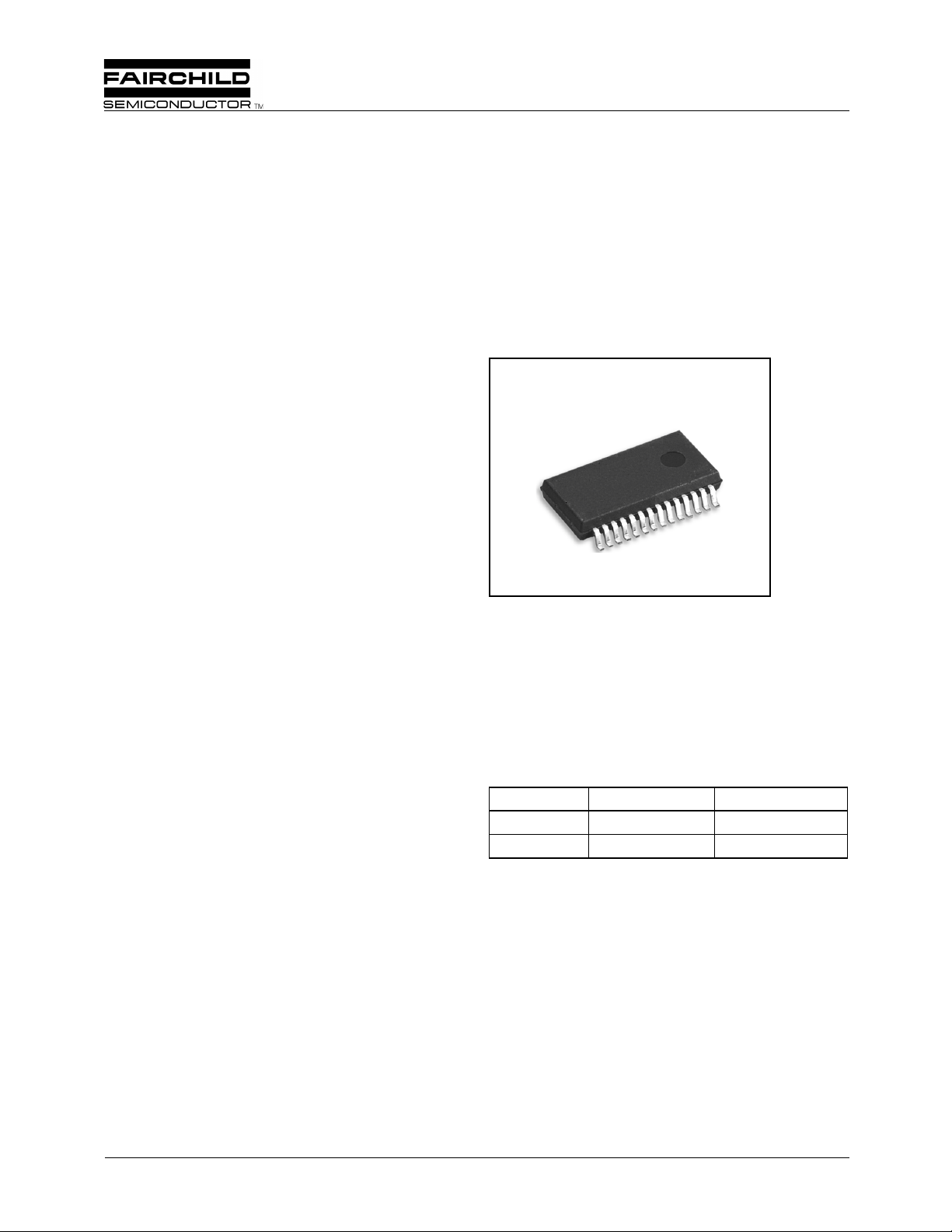
28-SSOP-300SG
Typical Applications
• Video cassette recorder (VCR) cylinder (drum) motor
• Other 2-phase BLDC motor
©2000 Fairchild Semiconductor International
Ordering Information
Device Package Operating Temp.
FAN8486D 28-SSOP-300SG −25°C ~ +75°C
FAN8486DTF 28-SSOP-300SG −25°C ~ +75°C
Rev. 1.0.1
February. 2000.
Page 2
FAN8486D (KA3086D)
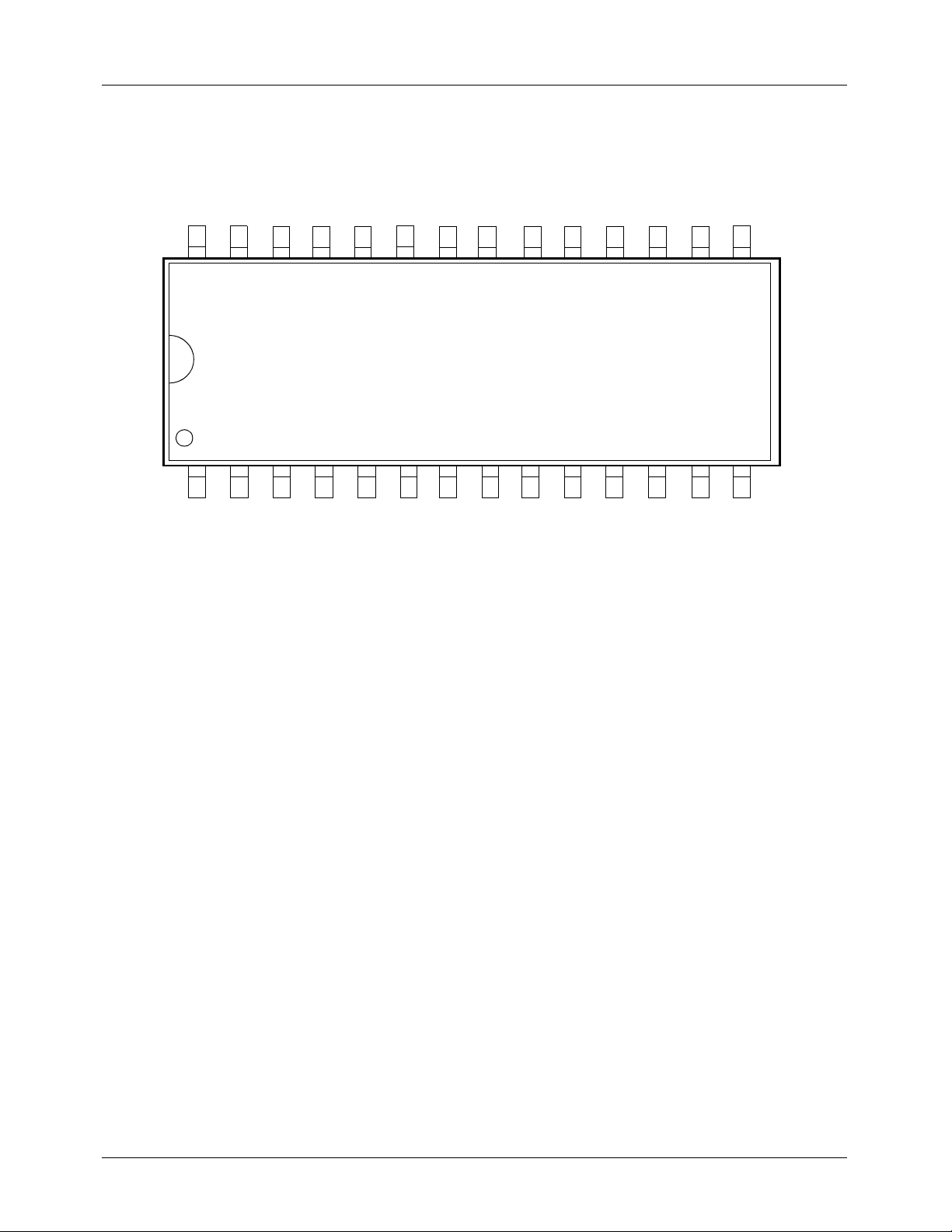
Pin Assignments
SGND
VCTL
H2P
FGAMPOUT
FGIN
FGOUT
VREG
PG(V25)
FG(V25)
PGAMPOUT
PGIN
1920212223242526
H2N
PGOUT
1428 27
161718
H1N
15
FAN8486D
23
14
NC
PVCC2
45 7 9
NC
NC
6
OUT2P
PGND2
8
OUT2N
OUT1P
PGND1
11
10
OUT1N
12
NC
PVCC1
14
13
H1P
SVCC
2
Rev. 1.0.1
February. 2000.
Page 3

Pin Definitions
Pine Number Pin Name I/O Pin Function Description
1 PVCC2 - Power supply voltage2
2NC -3NC -4NC -5 OUT2P O Output drive 2(P)
6 PGND2 O Power ground 2
7 OUT2N O Output drive 2(N)
8 OUT1P O Output drive 1(P)
9 PGND1 O Power ground 1
10 OUT1N - Output drive 1(N)
11 NC - 12 PVCC1 - Power supply voltage1
13 SVCC - Signal supply voltage
14 H1P I Hall signal input 1P
15 H1N I Hall signal input 1N
16 H2P I Hall signal input 2P
17 H2N I Hall signal input 2N
18 PGOUT O Phase generate output
19 PGAMPOUT O Phas e generate amp. output
20 PGIN I P hase generate input
21 PG(V25) - Reference voltage for PG
22 VREG - Regulated voltage
23 FG(V25) - Reference voltage for FG
24 FGIN I Frequency generate input
25 FGAMPOUT O Frequency generate amp. output
26 FGOUT O Frequency generate output
27 VCTL I Voltage control(motor speed control)
28 SGND - Signal ground
FAN8486D (KA3086D)
Rev. 1.0.1
February. 2000.
3
Page 4
FAN8486D (KA3086D)
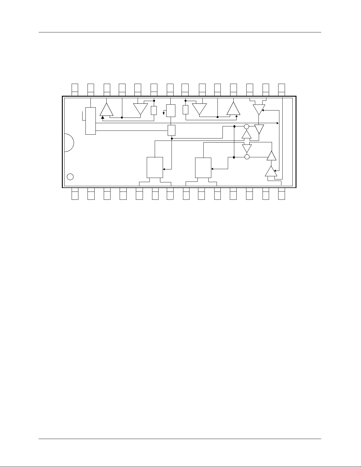
Internal Block Diagram
SGND
FGOUT
VCTL
H2P
FGIN
FG(V25)
VREG
FGAMPOUT
PG(V25)
PGAMPOUT
PGIN
1920212223242526
PGOUT
H2N
1428 27
161718
H1N
15
CTL
V
YS.
H
NC
COM
Control
NC
CTL
I
Current/Voltage
23
14
PVCC2
−
+
AMP
45 7 9
REF
REG
V
DRIVER
(5.0V)
V
Supply ea c h block
TSD
6
NC
OUT2P
PGND2
OUT2N
+
REF
V
8
OUT1P
AMP
-
HYS.
COM
DRIVER
10
11
NC
OUT1N
PGND1
+ -
±
AMP
GM
GM
±
12
PVCC1
13
+ -
SVCC
AMP
14
H1P
4
Rev. 1.0.1
February. 2000.
Page 5
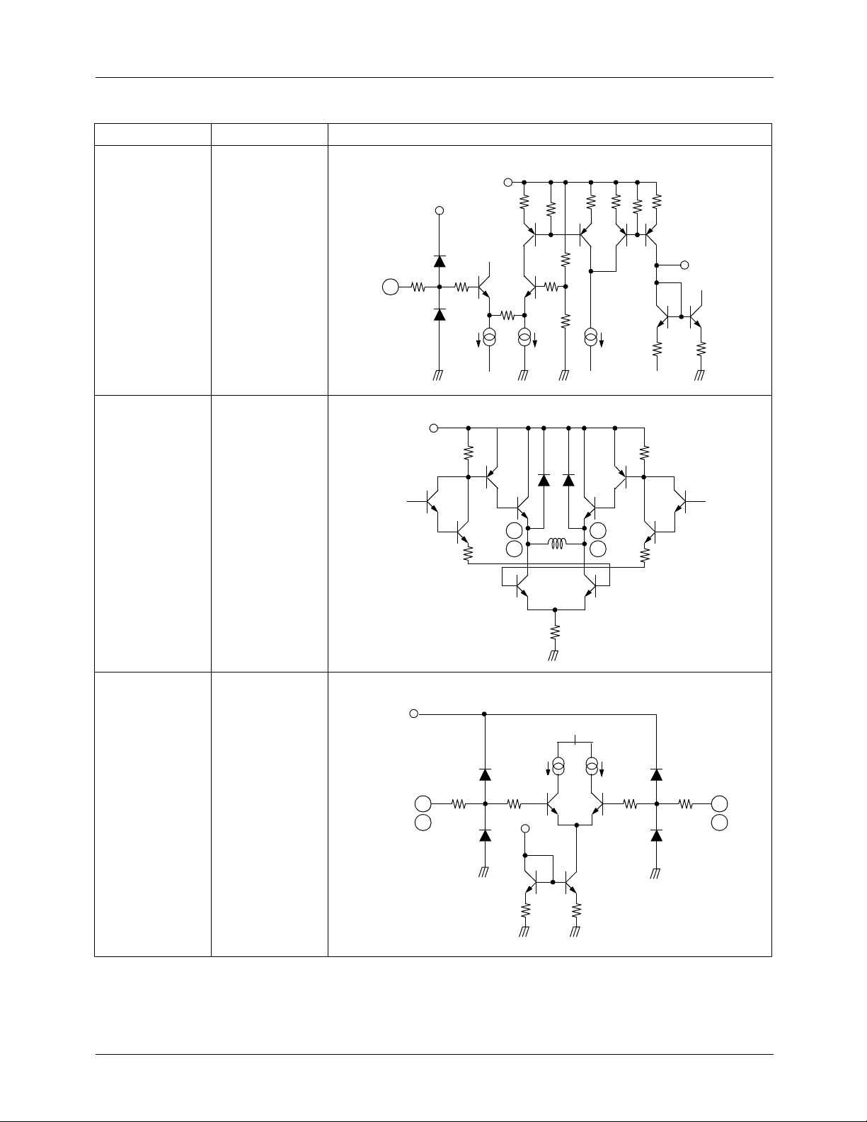
Equivalent Circuits
Description Pin No. Internal circuit
V
CTL
Motor output 5,7,8,10
27
V
REG
50
27
V
CC
1k
FAN8486D (KA3086D)
I
CTL
Hall input 14,15,16,17
V
REG
5
8
50
14
16
500
I
CTL
Vcc
7
10
500 50
15
17
Rev. 1.0.1
February. 2000.
5
Page 6

FAN8486D (KA3086D)
Equivalent Circuits (Continued)
Description Pin No. Internal circuit
PG, FG
amplifier
19,20
24,25
V
REG
PG, FG
hysteresis
amplifier
18,19,25,26
V
CC
50
20
24
V
REG
50
19
25
1k
V
CC
V
25
V
REG
V
25
V
CC
50
19
25
V
CC
50
18
26
6
Rev. 1.0.1
February. 2000.
Page 7

FAN8486D (KA3086D)
Absolute Maximum Ratings (Ta=25°°°°C)
Parameter Symbol Value Unit Remark
Supply voltage V
Maxium output current I
output current I
V
REG
Power dissipation P
Operating temperature T
Storage temperature T
Notes:
1. Duty 1 / 100, pulse wid th 50 0µs
2. 1) When mounted on glass epoxy PCB (76.2 × 114 × 1.57mm)
2) Power dissipation reduces 8.0mW /
3) Do not exceed Pd and SOA(Safe Operating Area).
CCmax
Omax
REGmax
d
OPR
STG
°C for using above Ta=25°C. (Without heat-sink)
18 V -
note1
1.0
A-
30 mA -
note2
1
W No heat sink
−25 ~ +75 °C-
−45 ~ +125 °C-
Power Dissipation Curve
Pd (mW)
2, 000
SOA
0
0 25 50 75 100 125
Recommened Operating Conditions (Ta=25°°°°C)
Parameter Symbol Min. Typ. Max Unit
Operating supply voltage V
CC
81216V
150 175
Ambient temperature, Ta [°C]
Rev. 1.0.1
February. 2000.
7
Page 8

FAN8486D (KA3086D)
Electrical Characteristics
(Ta=25°C, VCC=12V, unless otherwise specified)
Parameter Symbol Condition Min. Typ. Max. Unit
FULL CIRCUIT
Quiescent current I
VOLTAGE REGULATOR
Regulated voltage V
Regulated voltage V
HALL INPUT
Hall minimum input level
note
Hall bias current I
OUTPUT DIRVE
Output saturation voltage (Upper) V
Output saturation voltage (Lower) V
Output current A I
Output current B I
VOLTAGE CONTROL
reference voltage
V
CTL
V
injput range
CTL
offset range V
V
CTL
V
input bias current I
CTL
note
note
Q
REG
REG
V
INH
BH
SU
SL
OUTA
OUTB
V
25
V
CTL
OFF
VCTL
VCC=12V - 8.5 13 mA
VCC=12V 4.6 5.0 5.4 V
VCC=12V, I
=−20mA 4.6 5.0 5.4 V
REG
-50--mVp-p
V
=2.0V, Hall=2.5V - 0.25 2.0 µA
CTL
V
=4.5V - 1.3 2.0 V
CTL
V
=4.5V - 2.0 2.0 V
CTL
V
=2.6V
H1P
V
HALL_1N
V
H2P
V
H2N
0.48 × V
=2.4V, V
=2.6V
=2.4V, V
REG
CTL
CTL
=2.5V
=3.5V
-0-V
V
=0 ~ V
V
V
∆I
V
V
CTL
CTL
CTL
O
H1P
H1N
/ ∆V
CTL
=2.5V - 1.0 6.0 µA
=2.8V, 3.3V
CTL
=2.6V,
=2.4V
500 700 900 mA
500 700 900 mA
2.0 2.3 2.5 V
REG
V
−150 0 +150 mV
I
Voltage control gain G
NOTE:
The note in the chart means items calculated and approved in design not the items proven by actual test result.
M
8
O
0.48 × V
February. 2000.
0.55A/V(TYP)
(TYP) V
REG
Rev. 1.0.1
0.38 0.55 0.64 A / V
CTL
Page 9

Electrical Characteristics (Continued)
(Ta=25°C, VCC=12V, unless otherwise specified)
Parameter Symbol Condition Min. Typ. Max. Unit
FULL CIRCUIT
Shutdown temperature
Temperature hysteresis
FG / PG AMP
Input offset voltage V
Input current I
Open loop gain
note
Output high voltage V
Output low voltage V
COMPARATOR (HYSTERESIS)
Hysteresis level V
Output low voltage V
Output pull-up resistance V
note
note
TSD - 130 160 - °C
T
HYS
OFS
AMP_IN
G
OHA
OLA
HYS
OLHYS
BHYS
VIN=2.5V - 0.2 2.0 µA
VCC=12V, Signal=500Hz 65 70 - dB
A
VIN=2.0V
VIN=2.7 - 0.85 1.45 V
VIN=2.0V - 0.12 0.32 V
FAN8486D (KA3086D)
--30-°C
--0± 8mV
V
REG
−1.48
V
REG
−0.74
-V
- ±130 ±165 ±200 mV
- 7.0 10 13 kΩ
NOTE:
The note in the chart means items calculated and approved in design not the items proven by actual test result.
Rev. 1.0.1
February. 2000.
9
Page 10

FAN8486D (KA3086D)
Application Informations
1. A Diagram Summarizing The Entire System
I
V
TSD
C
AMP. DRIVER
REG
HALL+
HALL−
V
CTL
Hall_IN
V / I
Converter
I
C
I
4I
C
4I
C
2I
C
I
f
G
M
O
R2
FG_OUT
PG_OUT
FG_IN
PG_IN
R1
AMP &
COMP
AMP &
COMP
Figure 1.
Figure 1 is a conceptual diagram of the FAN8486D. It turns on or off depending on the signal of the hall sensor used for sensing the rotor position of motor.
The AMP, G
(Feedback) and output blocks are circuits used to determine current gain of FAN8486D.
M
Furthermore, HallIN represents the hall signal switch.
It supplies stable bias to each V
block. The TSD block is a thermal shutdown circuit that protects the IC during an high
REG
temperature inside the IC.
Moreover, FG. and PG. blocks output individual signals generated in the motor using the amplifier and comparator.
These signals transmit motor speed and position data to controller of external servo etc. for their control.
2. Current Control
Figure 2 simplifies figure 1.
The supplied I
Figure 3 is a graph of I
10
current drives the motor and the Ic current controls the motor speed.
O
vs. IO.
CTL
Rev. 1.0.1
February. 2000.
Page 11

I
CTL
I
Omax
FAN8486D (KA3086D)
I
O
A
T
Figure 2.
I
O
A
T
I
COmax
I
CTL
Figure 3.
3. Voltage Control
Even though FAN8486D command uses Ic to control the magnitude of IO, it can also use voltage. FAN8486D mainly uses
voltage cont rol and has op tion to use current control.
I
V
CTL
V / I
Converter
CTL
Figure 4 shows the principle of the voltage control.
The V
Figure 5 shows the graph of V
is the motor speed control voltage, and the I
CTL
vs. IO.
CTL
A
T
Figure 4.
is converted to current through the V / I converter.
CTL
I
O
I
Omax
I
O
A
0.48 × V
T
REG
(TYP)
G
M
V
CTL
Figure 5.
Rev. 1.0.1
February. 2000.
11
Page 12

FAN8486D (KA3086D)
Typical Performance Characteristics
5.0
4.0
(V)
3.0
REG
V
2.0
1.0
0.0
0 2 4 6 8 101214161820
V
(V)
CC
1.VCC vs V
12
10
8
(mA)
6
CC
I
4
2
0
8 1012141618
V
(V)
CC
3.VCC vs I
CC
V
REG
V
V
CTL
RL = 10 KΩ
RL = 10KΩ
CTL
= 3.5V
= 3.5V
CTL
= 0V
5
4
(V)
3
REG
V
2
V
= 0V
1
0
-30-20-10 0 10 20 30 40 50 60 70 80 90
Temperature(℃)
Temperature(°C)
2.Temp. vs V
0.63
0.58
0.53
0.48
GM1(A/V)
0.43
0.38
8 1012141618
V
(V)
CC
V
REG
V
CTL
CC
CTL
= 12V
= 3.5V
4.VCC vs GM1
12
900
850
800
750
700
(mA)
O
I
650
600
550
500
8 1012141618
(V)
V
CC
5.V
vs IOA
CC
V
= 3.5V
CTL
V
= 3.5V
CTL
RL = 10KΩ
RL = 10KΩ
900
850
800
750
700
(mA)
O
I
650
600
550
500
8 1012141618
Rev. 1.0.1
February. 2000.
V
6.V
CC
(V)
CC
V
RL = 10KΩ
vs IOB
= 3.5V
V
= 3.5V
CTL
CTL
RL = 10KΩ
Page 13

Test Circuits
V
CC
I
CC
FAN8486D (KA3086D)
1
PVCC2
2
NC
SGND
VCTL
28
27
VCTL
SW24
1
A
2
3
FGOUT
2mA
1
2
10Ω(20W)
1
2
1
2
Ω
(20W)
10
1
2
NC
3
NC
4
SW1
SW2
SW3
SW4
OUT2P
5
6
PGND2
7
OUT2N
OUT1P
8
PGND1
9
OUT1N
10
NC
11 18
PVCC1 H2N
12 17
FGOUT
FGAMPOUT
F
A
N
8
4
8
FG(V25)
6
D
PG(V25)
PGAMPOUT
PGOUT
FGIN
VREG
PGIN
26
SW23
3
2
1
I
REG
SW13
SW15
SW17
1
2
1
2
1
2
1
=−20µA
2
1
2
~
~
1
2
H2N
SW22
25
24
23
22
21
20
19
2
1
SW19
SW21
SW18
SW25
SW10
500µA
FGAMPOUT
2
SW20
1
FG(V25)
PG(V25)
1
2
3
1
SW16
2
1
A
2
3
−
500µA
FGIN
PGOUT
2mA
−
500µA
−
500µA
VREG
SW14
1
2
PGIN
PGAMPOUT
H1P
SW7
+
−
SW8
~
H1N
1
SW5
2
2
SW6
1
SVCC H2P
13 16
H1P H1N
14 15
SW9
1
2
Rev. 1.0.1
February. 2000.
SW12
SW11
H2P
−
+
~
13
Page 14

FAN8486D (KA3086D)
Typical Application Circuits
1
PVCC2
2
NC
NC
3
NC
4
OUT2P
5
SGND
VCTL
FGOUT
FGAMPOUT
F
A
FGIN
28
27
26
25
24
N
6
PGND2
8
FG(V25)
4
23
8
7
OUT2N
M
OUT1P
8
PGND1
9
6
VREG
D
PG(V25)
PGIN
22
21
PG
20
OUT1N
10
NC
11 18
PVCC1 H2N
12 17
SVCC H2P
13 16
H1P H1N
14 15
PGAMPOUT
PGOUT
19
V
REG
HALL
HALL
14
Rev. 1.0.1
February. 2000.
Page 15

FAN8486D (KA3086D)
Rev. 1.0.1
February. 2000.
15
Page 16

FAN8486D (KA3086D)
DISCLAIMER
FAIRCHILD SEMICONDUCTOR RESERVES THE RIGHT TO MAKE CHANGES WITHOUT FURT HER NOTICE TO ANY
PRODUCTS HEREI N TO IMPROVE RELIABILITY, FUNCTIO N OR DESIGN. FAIRCH IL D DOES NOT ASSUME ANY
LIABILITY ARISING OUT OF THE APPLICATION OR USE OF ANY PRODUCT OR CIRCUIT DESCRIBED HEREIN; NEITHER
DOES IT CONVEY ANY LICENSE UNDER IT S PATENT RIGHTS, NOR THE RIGHTS OF OTHE RS.
LIFE SUPPORT POL I CY
FAIRCHILD’S PR ODUCTS ARE NOT AUTH ORIZED FOR USE AS C RITICAL COMPONENT S IN LIFE SUPPORT DE VICES
OR SYSTEMS WITHOUT THE EXPRESS WRITTEN APPROVAL OF THE PRESIDENT OF FAIRCHILD SEMICONDUCTOR
INTERNATIONAL. As used herein:
1. Life support devices or systems are devices or systems
which, (a) are intended for surgical implant into the body,
or (b) support or sustain life, and (c) whose failure to
perform when properly used in accordance with
2. A critical component in any component of a life support
device or sy stem whose fai lure to perform can be
reasonably expec ted to cause the failur e of the life support
device or system, or to affect its safety or effec t iv ene ss .
instructions for use provided in the labeling, can be
reasonably expected to result in a significant injury of the
user.
www.fairchildsemi.com
12/1/00 0.0m 001
2000 Fairchild Semiconductor International
Stock#DSxxxxxxxx
 Loading...