

FAN5902
800mA Buck Converter for 3G RFPAs
FAN5902 — 800mA Buck Converter for 3G RFPAs FAN5902 — 800mA Buck Converter for 3G RFPAs
May 2009
Features
92% Efficient Synchronous Operation
2.7V to 5.5V Input Voltage Range
V
Range from 0.4V to 3.4V (or VIN)
OUT
Up to 800mA Output Current
20µs Step Response
30µs Bypass Transition Time
50mΩ Integrated Bypass FET with Controlled Slew
Rate for Low Battery Voltage Operation
6MHz PWM Operation Allows 470nH Small Form
Factor Inductor
100% Duty Cycle for Low Dropout Operation
Thermal Shutdown
Input Under-Voltage Lockout
12-Lead MLP (0.8mm Maximum)
12-Bump WLCSP
Applications
Battery-Powered 3G RFPAs
Multiband/Multimode WCDMA/CDMA Handset RF
Transceivers
RF PC Cards
Pocket PC and PDAs with Communication
Capabilities
Description
The FAN5902 is a high-efficiency, low-noise,
synchronous, step-down DC-to-DC converter designed
for powering the radio frequency power amplifiers
(RFPA) in 3G mobile handsets and other mobile
applications. It provides up to 800mA of output current
over an input voltage range of 2.7V to 5.5V. The output
voltage can be dynamically adjusted from 0.4V up to
3.4V, proportional to an analog input voltage ranging
from 0.2V to 1.7V provided by an external DAC. This
allows supplying the RFPA with the voltage level that
provides optimum Power Added Efficiency (PAE).
An integrated bypass FET automatically switches on
when the battery voltage drops too close to the output
voltage (when V
transition is controlled by a slew rate controller to limit
the inrush current and reduce the RFPA gain deviation.
The FAN5902 offers fast transition times, allowing
changes to the output voltage in less than 20µs.
The FAN5902 operates at 6MHz, enabling the use of a
small, low-value inductor of 470nH. A current-mode
control loop with fast transient response ensures
excellent line and load regulation.
The FAN5902 improves the RFPA power efficiency and
increases the talk/connection time in 3G handsets.
The FAN5902 is available in a 12-lead MLP package
and 12-bump WLCSP.
OUT=VBAT
-250mV). The bypass
Important
For complete performance specifications and
datasheet, please contact a Fairchild Semiconductor
sales representative.
Ordering Information
Part Number
FAN5902MPX -40 to +85°C
FAN5902UCX -40 to +85°C
For Fairchild’s definition of Eco Status, please vis it: http://www.fairchildsemi.com/company/green/rohs_green.html.
© 2009 Fairchild Semiconductor Corporation www.fairchildsemi.com
FAN5902 • Rev. 1.0.2.short
Operating
Temperature Range
Package
12-Lead, 3x3.5mm, Molded Leadless
Package (MLP)
12-Bump, Wafer-Level Chip-Scale
Package (WLCSP)
Eco Status
RoHS Tape and Reel
RoHS
Packing
Method
Tape and Reel
FAN5902 — 800mA Buck Converter for 3G RFPAs
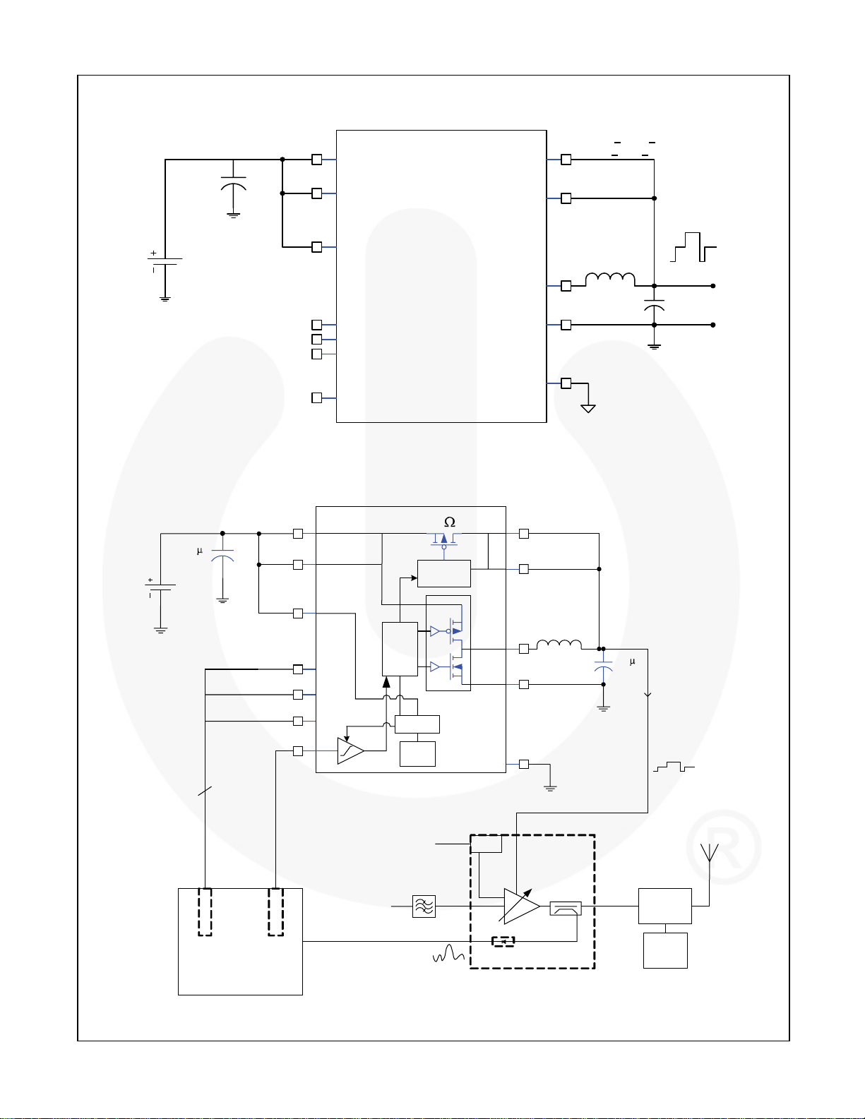
Application Diagrams
10μF
V
BAT
2.7V to
5.5V
From Processor
From External DAC
PVIN
PVIN VOUTSNS
PVIN
VOUTSNS
AVIN
FAN5902
BPE N
SW
PGND
SYNC
EN
AGND
VCON
Figure 1. FAN5902 Circuit
DCDC
V
50m
OUT_SNS
0.4V < V
20mA < I
470nH
OUT
OUT
< V
BAT
< 800mA
V
2.2μF
OUT
10 F
0603
V
BATT
2.7V up to 5.5V
3
G
P
I
O
Processor
Base
PVIN
AVIN
BPE N
SYNC
EN
VCON
D
A
C
Bypass Sl ew
Controller
Swi tcher
Controller
SW
PGND
V
Reference
Bandgap
V
MOD E
R
FIN
P
DET
Bias
Power
Detector
AGND
RFPA
Figure 2. Typical Application
OUT_SNS
470n H
Supply
V
OUT
2.2 F
0603
0.4V up to V
Up to 800mA
V
Dynamic
Scaling
R
FOUT
Duplexer
RX
IN
OUT
© 2009 Fairchild Semiconductor Corporation www.fairchildsemi.com
FAN5902 • Rev. 1.0.2.short 2
Pin Configurations
Figure 3. 12-Lead MLP
(Top View)
FAN5902 — 800mA Buck Converter for 3G RFPAs
Figure 4. 12-Bump WLCSP
(Top View)
Pin Definitions
MLP
Pin #
(*) (*) AGND
VOUTSNS
EN
VCON Analog control input from an external D-to-A converter.
AVIN Analog bias supply voltage input. Connect to PVIN.
AGND Connect to analog ground.
BPEN
SYNC
PGND
SW Switching node of the internal MOSFET switches. Connect to output inductor.
PVIN
(*) Pinout available upon request
WLCSP
Pin #
Name Description
Analog ground, reference ground for the IC. Follow PCB routing notes for
connecting this pin.
Output voltage sense pin. Connect to V
regulation.
Enables switcher when HIGH, shutdown mode when LOW. This pin should not
be left floating.
Force bypass transistor when HIGH; auto-bypass when LOW. This pin should
not be left floating
External clock synchronization input and PFM lockout. When SYNC remains
HIGH, the DC-to-DC does not allow PFM mode. Tie SYNC to AGND if not used.
Power ground of the internal MOSFET switches. Follow routing notes for
connections between PGND and AGND.
Supply voltage input to the internal MOSFET switches. Connect to input power
source.
to establish feedback path for
OUT
© 2009 Fairchild Semiconductor Corporation www.fairchildsemi.com
FAN5902 • Rev. 1.0.2.short 3

FAN5902 — 800mA Buck Converter for 3G RFPAs
Absolute Maximum Ratings
Stresses exceeding the absolute maximum ratings may damage the device. The device may not function or be
operable above the recommended operating conditions and stressing the parts to these levels is not recommended.
In addition, extended exposure to stresses above the recommended operating conditions may affect device
reliability. The absolute maximum ratings are stress ratings only.
Symbol Parameter Min. Max. Unit
VIN
TJ Junction Temperature -40 +125 °C
T
STG
TL Lead Soldering Temperature (10 Seconds) +260 °C
θJC Thermal Resistance, Junction to Tab
θJC Thermal Resistance, Junction to Case
1. Refer to θJA data below.
AVIN, PVIN -0.3 6.0
Voltage On Any Other Pin -0.3 AV
IN
+0.3
V
Storage Temperature -65 +150 °C
(1)
MLP Package 5 °C/W
(1)
WLCSP Package 30 °C/W
Recommended Operating Conditions
The Recommended Operating Conditions table defines the conditions for actual device operation. Recommended
operating conditions are specified to ensure optimal performance to the datasheet specifications. Fairchild does not
recommend exceeding them or designing to Absolute Maximum Ratings.
Symbol Parameter Min. Typ. Max. Unit
VCC
V
OUT
I
OUT
CIN
C
OUT
TA
TJ
Notes:
2. A high input capacitor value is required for limiting input voltage drop during bypass transitions or during large
3. Refer to application note AN-6087 for more details.
Dissipation Ratings
Molded Leadless Package (MLP) 49ºC/W
Wafer-Level Chip-Scale Package (WLCSP) 110ºC/W
Notes:
4. Thermal Resistance, Junction-to-Ambient, measured according to JEDEC 2S2P PCB (and zero air flow). θJA for
5. Maximum power dissipation is a function of T
Supply Voltage Range 2.7 5.5 V
Output Voltage Range 0.4 V
Output Current 20 800 mA
L
Inductor 0.47 µH
Input Capacitor
Output Capacitor
(2)
10 µF
(2)
2.2 4.7 10.0 µF
V
IN
Operating Ambient Temperature Range -40 +85 °C
Operating Junction Temperature Range -40 +125 °C
output voltage transitions. Ensure the input capacitor value is greater than the output capacitor’s. See the inrush
current specifications below.
(4)
Package θ
(4)
JA
(5)
2050mW 21mW/ºC
(5)
900mW 9mW/ºC
Power Rating
at T
≤ 25°C
A
(5)
Derating Factor
> TA=25ºC
JEDEC 1S0P PCB (and zero air flow) = 210°C/W.
, θJA, and TA. The maximum allowable power dissipation at any
allowable ambient temperature is P
D
=[T
J(max)
- TA ] / θJA.
J(max)
© 2009 Fairchild Semiconductor Corporation www.fairchildsemi.com
FAN5902 • Rev. 1.0.2.short 4

Typical Performance Characteristics
Typical performance at 25°C.
500
FAN5902 — 800mA Buck Converter for 3G RFPAs
30
PAE with FAN5902
250
[mA]
BAT
I
I
without FAN5902
BAT
I
wi th FAN5902
P
OUT
BAT
[dBm]
0
01530
Figure 5. Comparison of RF PA Current Consumption
with and without FAN5902
15
PAE [%]
PAE without FAN5902
0
01530
P
[dBm]
OUT
Figure 6. Comparison of RFPA Power Added
Efficiency with and without FAN5902
Figure 7. Rise Times for 300mV, 500mV, and 2V ΔV
C
= 2.2µF (VIN=3.7V)
OUT
OUT
Figure 8. Rise Times for 300mV, 500mV, and 2V
ΔV
OUT COUT
= 2.2µF (VIN=3.7V)
© 2009 Fairchild Semiconductor Corporation www.fairchildsemi.com
FAN5902 • Rev. 1.0.2.short 5

Physical Dimensions
2X
0.10
A
3.50
FAN5902 — 800mA Buck Converter for 3G RFPAs
A
B
2.60
PIN#1 IDENT
0.10
0.08
PIN#1 IDENT
0.25+/-0.05
C
C
0.05
0.00
0.45+/-0.05
(12X)
TOP VIEW
0.8 MAX
SIDE VIEW
2.60+/-0.05
1
0.50
BOTTOM VIEW
(0.38)
6
712
0.25+/-0.05 (12X)
3.00
0.10
B
2X
(0.2)
C
SEATING PLANE
1.60+/-0.05
0.10 CAB
0.05
C
2.65
1.85
1.05
0.85
0.85
2.84
LAND PATTERN RECOMMENDATION
NOTES:
A. CONFORMS TO JEDEC MO-229
VARIATION WFED-2.
B. DIMENSIONS ARE IN MILLIMETERS
C. DIMENSIONS AND TOLERANCES PER
ASME Y14.5M, 1994
D. LANDPATTERN RECOMMENDATION IS
BASED ON IPC 7351 DESIGN GUIDELINES
E. LANDPATTERN EXTENSION TO INCLUDE
CENTER PAD TABS IS OPTIONAL
F. FILENAME AND REV: MKT-MLP12DREV1
Figure 9: 3x3.5mm 12-Lead MLP
Package drawings are provided as a service to customers considering Fairchild components. Drawings may change in any manner
without notice. Pl ease note the revision and/or date on t he drawing and contact a Fairchild Semiconductor representative t o verify
or obtain the most recent revision. Package specifications do not expand the terms of Fairchild’s worldwide terms and conditions, specifically
the warranty therein, which covers Fairchild products.
Always visit Fairchild Semiconductor’s online packaging area for the most recent package drawings:
http://www.fairchildsem i.com/p ackagi ng/
© 2009 Fairchild Semiconductor Corporation www.fairchildsemi.com
FAN5902 • Rev. 1.0.2.short 6
.

Physical Dimensions (Continued)
FAN5902 — 800mA Buck Converter for 3G RFPAs
BALL A1
INDEX AREA
0.03 C
2X
E
A
B
(Ø0.25)
Cu PAD
A1
0.50
1.00
(Ø0.35)
D
0.50
SOLDER MASK
OPENING
C
2X
0.03 C
RECOMMENDED LAND PATTERN (NSMD)
0.332±0.018
0.250±0.025
0.05 C
D
TOP VIEW
C
0.06
0.625
0.539
SEATING PLANE
SIDE VIEWS
(X)+/-.018
0.50
0.005 CAB
12 X Ø0.315 +/- .025
A. NO JEDEC REGISTRATION APPLIES
B. DIMENSIONS ARE IN MILLIMETERS.
C. DIMENSIONS AND TOLERANCES PER
ASME Y14.5M, 1994
D
DATUM C, THE SEATING PLANE, IS DEFINED
BY THE SPHERICAL CROWNS OF THE BALLS.
F
FOR DIMENSIONS D, E, X, AND Y SEE
PRODUCT DATASHEET.
F. BALL COMPOSITION: Sn95.5Ag3.9Cu0.6
SAC405 ALLOY
(Y)+/-.018
0.50
12
BOTTOM VIEW
D
C
B
A
3
G. DRAWING FILENAME: MKT-UC012AArev2
Figure 10. 12-Bump WLCSP
Package drawings are provided as a service to customers considering Fairchild components. Drawings may change in any manner
without notice. Pl ease note the revision and/or date on t he drawing and contact a Fairchild Semiconductor representative t o verify
or obtain the most recent revision. Package specifications do not expand the terms of Fairchild’s worldwide terms and conditions, specifically
the warranty therein, which covers Fairchild products.
Always visit Fairchild Semiconductor’s online packaging area for the most recent package drawings:
http://www.fairchildsem i.com/p ackagi ng/
.
© 2009 Fairchild Semiconductor Corporation www.fairchildsemi.com
FAN5902 • Rev. 1.0.2.short 7

FAN5902 — 800mA Buck Converter for 3G RFPAs
© 2009 Fairchild Semiconductor Corporation www.fairchildsemi.com
FAN5902 • Rev. 1.0.2.short 8
 Loading...