

Page 1
EMC2DXV5T1,
EMC3DXV5T1,
EMC4DXV5T1,
EMC5DXV5T1
Preferred Devices
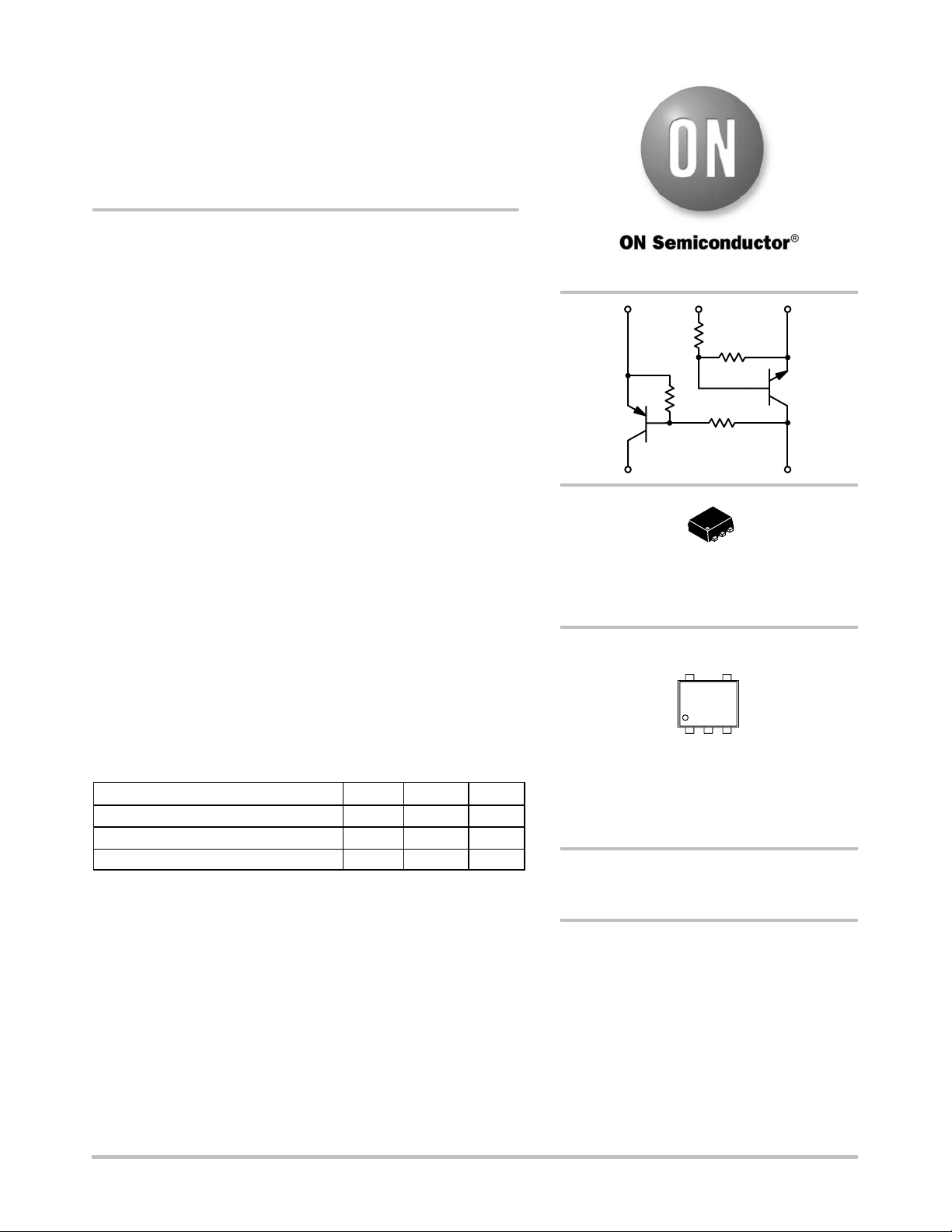
Dual Common
Base−Collector Bias
Resistor Transistors
NPN and PNP Silicon Surface Mount
Transistors with Monolithic Bias
Resistor Network
The BR T (Bias Resistor Transistor) contains a single transistor with
a monolithic bias network consisting of two resistors; a series base
resistor and a base−emitter resistor. These digital transistors are
designed to replace a single device and its external resistor bias
network. The BRT eliminates these individual components by
integrating them into a single device. In the EMC2DXV5T1 series,
two complementary BRT devices are housed in the SOT−553 package
which is ideal for low power surface mount applications where board
space is at a premium.
http://onsemi.com
312
R1
Q1
45
5
CASE 463B
R2
R1
SOT−553
R2
Q2
1
Features
• Simplifies Circuit Design
• Reduces Board Space
• Reduces Component Count
• These are Pb−Free Devices
MAXIMUM RATINGS (T
and Q2, − minus sign for Q1 (PNP) omitted)
Rating Symbol Value Unit
Collector-Base Voltage V
Collector-Emitter Voltage V
Collector Current I
Stresses exceeding Maximum Ratings may damage the device. Maximum
Ratings are stress ratings only. Functional operation above the Recommended
Operating Conditions is not implied. Extended exposure to stresses above the
Recommended Operating Conditions may affect device reliability.
= 25°C unless otherwise noted, common for Q
A
CBO
CEO
C
50 Vdc
50 Vdc
100 mAdc
1
MARKING DIAGRAM
Ux M G
G
Ux = Specific Device Code
x = C, 3, E, or 5
M = Date Code
G = Pb−Free Package
(Note: Microdot may be in either location)
ORDERING INFORMATION
See detailed ordering and shipping information in the package
dimensions section on page 2 of this data sheet.
Preferred devices are recommended choices for future use
and best overall value.
© Semiconductor Components Industries, LLC, 2007
April, 2007 − Rev. 5
1 Publication Order Number:
EMC2DXV5T1/D
Page 2
EMC2DXV5T1, EMC3DXV5T1, EMC4DXV5T1, EMC5DXV5T1
THERMAL CHARACTERISTICS
Characteristic Symbol Max Unit
ONE JUNCTION HEATED
Total Device Dissipation
TA = 25°C
Derate above 25°C
Thermal Resistance, Junction-to-Ambient
BOTH JUNCTIONS HEATED
Total Device Dissipation
TA = 25°C
Derate above 25°C
Thermal Resistance, Junction-to-Ambient
Junction and Storage Temperature TJ, T
1. FR−4 @ Minimum Pad
DEVICE ORDERING INFORMATION, MARKING AND RESISTOR VALUES
Transistor 1 − PNP Transistor 2 − NPN
Device Marking R1 (K) R2 (K) R1 (K) R2 (K) Package Shipping
EMC2DXV5T1
EMC2DXV5T1G SOT−553*
EMC2DXV5T5 SOT−553*
EMC2DXV5T5G SOT−553*
EMC3DXV5T1
EMC3DXV5T1G SOT−553*
EMC3DXV5T5 SOT−553*
EMC3DXV5T5G SOT−553*
EMC4DXV5T1
EMC4DXV5T1G SOT−553*
EMC4DXV5T5 SOT−553*
EMC4DXV5T5G SOT−553*
EMC5DXV5T1
EMC5DXV5T1G SOT−553*
EMC5DXV5T5 SOT−553*
EMC5DXV5T5G SOT−553*
†For information on tape and reel specifications, including part orientation and tape sizes, please refer to our Tape and Reel Packaging
Specifications Brochure, BRD8011/D.
*This package is inherently Pb−Free.
UC 22 22 22 22
U3 10 10 10 10
UE 10 47 47 47
U5 4.7 10 47 47
P
R
P
R
D
q
JA
D
q
JA
stg
SOT−553*
SOT−553*
SOT−553*
SOT−553*
357 (Note 1)
2.9 (Note 1)
mW
mW/°C
350 (Note 1) °C/W
500 (Note 1)
4.0 (Note 1)
mW
mW/°C
250 (Note 1) °C/W
− 55 to +150 °C
†
4000 / Tape & Reel
8000 / Tape & Reel
4000 / Tape & Reel
8000 / Tape & Reel
4000 / Tape & Reel
8000 / Tape & Reel
4000 / Tape & Reel
8000 / Tape & Reel
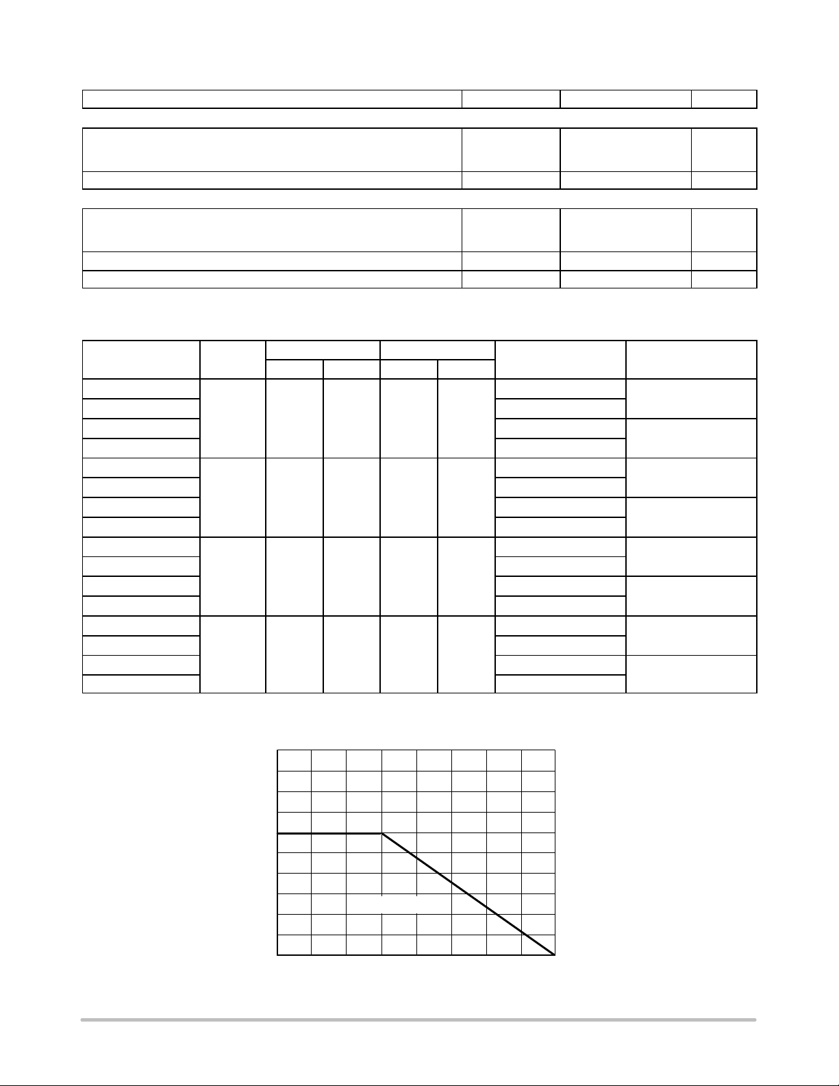
250
200
150
100
R
= 833°C/W
q
50
, POWER DISSIPATION (MILLIWATTS)
D
P
0
−50 0 50 100 150
JA
TA, AMBIENT TEMPERATURE (°C)
Figure 1. Derating Curve
http://onsemi.com
2
Page 3
EMC2DXV5T1, EMC3DXV5T1, EMC4DXV5T1, EMC5DXV5T1
ELECTRICAL CHARACTERISTICS (T
= 25°C unless otherwise noted)
A
Characteristic Symbol Min Typ Max Unit
Q1 TRANSISTOR: PNP
OFF CHARACTERISTICS
Collector-Base Cutoff Current (V
= 50 V, IE = 0) I
CB
Collector-Emitter Cutoff Current (VCB = 50 V, IB = 0) I
Emitter-Base Cutoff Current EMC2DXV5T1
(VEB = 6.0, IC = 5.0 mA) EMC3DXV5T1
EMC4DXV5T1
EMC5DXV5T1
ON CHARACTERISTICS
Collector-Base Breakdown Voltage (IC = 10 mA, IE = 0)
Collector-Emitter Breakdown Voltage (IC = 2.0 mA, IB = 0) V
DC Current Gain EMC2DXV5T1
(VCE = 10 V, IC = 5.0 mA) EMC3DXV5T1
EMC4DXV5T1
EMC5DXV5T1
Collector−Emitter Saturation Voltage (IC = 10 mA, IB = 0.3 mA) V
Output Voltage (on) (VCC = 5.0 V, V
Output Voltage (off) (VCC = 5.0 V, V
= 2.5 V, RL = 1.0 kW)
B
= 0.5 V, RL = 1.0 kW)
B
Input Resistor EMC2DXV5T1
EMC3DXV5T1, EMC4DXV5T1
EMC5DXV5T1
Resistor Ratio EMC2DXV5T1
EMC3DXV5T1
EMC4DXV5T1
EMC5DXV5T1
Q2 TRANSISTOR: NPN
OFF CHARACTERISTICS
Collector-Base Cutoff Current (VCB = 50 V, IE = 0) I
Collector-Emitter Cutoff Current (VCB = 50 V, IB = 0) I
Emitter-Base Cutoff Current EMC2DXV5T1
(VEB = 6.0, IC = 5.0 mA) EMC3DXV5T1
EMC4DXV5T1, EMC5DXV5T1
ON CHARACTERISTICS
Collector-Base Breakdown Voltage (IC = 10 mA, IE = 0)
Collector-Emitter Breakdown Voltage (IC = 2.0 mA, IB = 0) V
DC Current Gain EMC2DXV5T1
(VCE = 10 V, IC = 5.0 mA) EMC3DXV5T1
EMC4DXV5T1, EMC5DXV5T1
Collector−Emitter Saturation Voltage (IC = 10 mA, IB = 0.3 mA) V
Output Voltage (on) (VCC = 5.0 V, V
Output Voltage (off) (VCC = 5.0 V, V
= 2.5 V, RL = 1.0 kW)
B
= 0.5 V, RL = 1.0 kW)
B
Input Resistor EMC2DXV5T1
EMC3DXV5T1
EMC4DXV5T1, EMC5DXV5T1
Resistor Ratio EMC2DXV5T1
EMC3DXV5T1
EMC4DXV5T1, EMC5DXV5T1
CBO
CEO
I
EBO
V
(BR)CBO
(BR)CEO
h
FE
CE(SAT)
V
OL
V
OH
R1 15.4
R1/R2 0.8
CBO
CEO
I
EBO
V
(BR)CBO
(BR)CEO
h
FE
CE(SAT)
V
OL
V
OH
R1 15.4
R1/R2 0.8
− − 100 nAdc
− − 500 nAdc
−
−
−
−
−
−
−
−
0.2
0.5
0.2
1.0
mAdc
50 − − Vdc
50 − − Vdc
60
35
80
20
100
60
140
35
−
−
−
−
− − 0.25 Vdc
− − 0.2 Vdc
4.9 − − Vdc
7.0
3.3
0.8
0.17
0.38
22
10
4.7
1.0
1.0
0.21
0.47
28.6
13
6.1
1.2
1.2
0.25
0.56
− − 100 nAdc
− − 500 nAdc
−
−
−
−
−
−
0.2
0.5
0.1
mAdc
50 − − Vdc
50 − − Vdc
60
35
80
100
60
140
−
−
−
− − 0.25 Vdc
− − 0.2 Vdc
4.9 − − Vdc
7.0
33
0.8
0.8
22
10
47
1.0
1.0
1.0
28.6
13
61
1.2
1.2
1.2
kW
kW
http://onsemi.com
3
Page 4
EMC2DXV5T1, EMC3DXV5T1, EMC4DXV5T1, EMC5DXV5T1
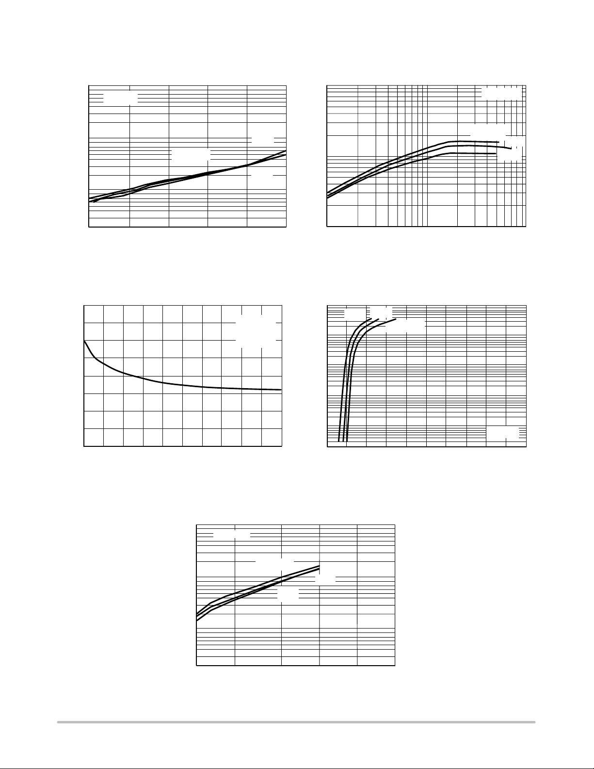
TYPICAL ELECTRICAL CHARACTERISTICS − EMC2DXV5T1 PNP TRANSISTOR
10
IC/IB = 10
1
TA=−25°C
0.1
0.01
, COLLECTOR EMITTER SATURATION VOLTAGE (V)
0 20 50
CE(sat)
V
4
3
2
IC, COLLECTOR CURRENT (mA)
Figure 2. V
CE(sat)
versus I
C
25°C
75°C
40
f = 1 MHz
lE = 0 mA
TA = 25°C
1000
100
, DC CURRENT GAIN
FE
10
100
VCE = 10 V
TA=75°C
25°C
−25°C
1
IC, COLLECTOR CURRENT (mA)
10
100
Figure 3. DC Current Gain
25°C
75°C
10
1
TA=−25°C
, CAPACITANCE (pF)
ob
C
0.1
1
0
VR, REVERSE BIAS VOLTAGE (V)
Figure 4. Output Capacitance
, INPUT VOLTAGE (VOLTS)
in
V
100
10
0.1
VO = 0.2 V
TA=−25°C
1
0 10 20 30
IC, COLLECTOR CURRENT (mA)
50010 203040
75°C
, COLLECTOR CURRENT (mA) h
C
I
0.01
0.001
0 1 2 3 4
Vin, INPUT VOLTAGE (V)
5 6 7 8 9 10
Figure 5. Output Current versus Input Voltage
25°C
40 50
VO = 5 V
Figure 6. Input Voltage versus Output Current
http://onsemi.com
4
Page 5

EMC2DXV5T1, EMC3DXV5T1, EMC4DXV5T1, EMC5DXV5T1
TYPICAL ELECTRICAL CHARACTERISTICS − EMC2DXV5T1 NPN TRANSISTOR
1
IC/IB = 10
0.1
0.01
0.001
020 4050
, COLLECTOR EMITTER SATURATION VOLTAGE (V)
CE(sat)
V
4
3
2
, CAPACITANCE (pF)
ob
1
C
0
010203040
IC, COLLECTOR CURRENT (mA)
Figure 7. V
VR, REVERSE BIAS VOLTAGE (V)
CE(sat)
TA=−25°C
versus I
25°C
75°C
C
f = 1 MHz
IE = 0 mA
TA = 25°C
1000
VCE = 10 V
TA=75°C
25°C
−25°C
100
, DC CURRENT GAIN
FE
10
1 10 100
IC, COLLECTOR CURRENT (mA)
Figure 8. DC Current Gain
100
75°C
10
1
0.1
0.01
, COLLECTOR CURRENT (mA) h
C
I
50
0.001
01 234
25°C
TA=−25°C
VO = 5 V
56 78 910
Vin, INPUT VOLTAGE (V)
Figure 9. Output Capacitance
10
VO = 0.2 V
1
, INPUT VOLTAGE (VOLTS)
in
V
0.1
Figure 11. Input Voltage versus Output
Figure 10. Output Current versus Input Voltage
TA=−25°C
25°C
75°C
1002030
IC, COLLECTOR CURRENT (mA)
40 50
Current
http://onsemi.com
5
Page 6

EMC2DXV5T1, EMC3DXV5T1, EMC4DXV5T1, EMC5DXV5T1
TYPICAL ELECTRICAL CHARACTERISTICS − EMC3DXV5T1 PNP TRANSISTOR
1
IC/IB = 10
0.1
0.01
, COLLECTOR EMITTER SATURATION VOLTAGE (V)
0 40
CE(sat)
V
4
3
2
20
IC, COLLECTOR CURRENT (mA)
Figure 12. V
CE(sat)
TA=−25°C
75°C
versus I
25°C
C
f = 1 MHz
lE = 0 mA
TA = 25°C
1000
100
, DC CURRENT GAIN
FE
h
10
50
1 10 100
IC, COLLECTOR CURRENT (mA)
VCE = 10 V
TA=75°C
25°C
−25°C
Figure 13. DC Current Gain
100
75°C
10
1
25°C
TA=−25°C
, CAPACITANCE (pF)
ob
1
C
0
010203040
VR, REVERSE BIAS VOLTAGE (V)
Figure 14. Output Capacitance Figure 15. Output Current versus Input
100
VO = 0.2 V
10
1
, INPUT VOLTAGE (VOLTS)
in
V
0.1
0
0.1
, COLLECTOR CURRENT (mA)
C
0.01
I
50
10 20 30 40 50
IC, COLLECTOR CURRENT (mA)
0.001
0
TA=−25°C
75°C
1 2 3 4 5 6 7 8 9 10
25°C
VO = 5 V
Vin, INPUT VOLTAGE (V)
Voltage
Figure 16. Input Voltage versus Output
Current
http://onsemi.com
6
Page 7

EMC2DXV5T1, EMC3DXV5T1, EMC4DXV5T1, EMC5DXV5T1
TYPICAL ELECTRICAL CHARACTERISTICS − EMC3DXV5T1 NPN TRANSISTOR
1
IC/IB = 10
0.1
0.01
0.001
, COLLECTOR EMITTER SATURATION VOLTAGE (V)
0
CE(sat)
V
4
3
2
, CAPACITANCE (pF)
ob
1
C
0
0 10 203040
TA=−25°C
20 50
IC, COLLECTOR CURRENT (mA)
Figure 17. V
VR, REVERSE BIAS VOLTAGE (V)
CE(sat)
25°C
versus I
75°C
40
C
f = 1 MHz
IE = 0 mA
TA = 25°C
1000
100
, DC CURRENT GAIN
FE
10
1 100
IC, COLLECTOR CURRENT (mA)
10
VCE = 10 V
TA=75°C
25°C
−25°C
Figure 18. DC Current Gain
100
10
1
0.1
, COLLECTOR CURRENT (mA) h
0.01
C
I
0.001
50
0
246810
75°C 25°C
TA=−25°C
VO = 5 V
Vin, INPUT VOLTAGE (V)
Figure 19. Output Capacitance Figure 20. Output Current versus Input Voltage
100
VO = 0.2 V
TA=−25°C
, INPUT VOLTAGE (VOLTS)
in
V
0.1
10
75°C
1
0
10 20 30 40 50
IC, COLLECTOR CURRENT (mA)
25°C
Figure 21. Input Voltage versus Output
Current
http://onsemi.com
7
Page 8

EMC2DXV5T1, EMC3DXV5T1, EMC4DXV5T1, EMC5DXV5T1
e
TYPICAL ELECTRICAL CHARACTERISTICS −EMC4DXV5T1 PNP TRANSISTOR
1
IC/IB = 10
0.1
0.01
0.001
, COLLECTOR EMITTER SATURATION VOLTAGE (V)
020406080
CE(sat)
V
4.5
4
3.5
3
2.5
2
1.5
, CAPACITANCE (pF)
ob
C
1
0.5
0
0 2 4 6 8101520253035404550
IC, COLLECTOR CURRENT (mA)
Figure 22. V
VR, REVERSE BIAS VOLTAGE (V)
CE(sat)
TA=−25°C
75°C
versus I
25°C
C
f = 1 MHz
lE = 0 V
TA = 25°C
180
VCE = 10 V
160
140
120
100
80
60
40
, DC CURRENT GAIN (NORMALIZED)
20
FE
0
1 10 100
2 4 6 8 15 20 40 50 60 70 80 90
IC, COLLECTOR CURRENT (mA)
−25°C
TA=75°C
25°C
Figure 23. DC Current Gain
100
TA=75°C
−25°C
10
, COLLECTOR CURRENT (mA) h
C
I
1
0 246810
Vin, INPUT VOLTAGE (V)
VO = 5 V
25°C
Figure 24. Output Capacitance Figure 25. Output Current versus Input Voltage
10
VO = 0.2 V
75°C
1
, INPUT VOLTAGE (VOLTS)
in
V
0.1
010 20 30 4050
IC, COLLECTOR CURRENT (mA)
25°C
TA=−25°C
Figure 26. Input Voltage versus Output Current
http://onsemi.com
+12 V
Typical Application
for PNP BRTs
LOAD
Figure 27. Inexpensive, Unregulated Current Sourc
8
Page 9

EMC2DXV5T1, EMC3DXV5T1, EMC4DXV5T1, EMC5DXV5T1
TYPICAL ELECTRICAL CHARACTERISTICS − EMC5DXV5T1 PNP TRANSISTOR
1
IC/IB = 10
TA=75°C
0.1
0.01
, COLLECTOR EMITTER SATURATION VOLTAGE (V)
0
CE(sat)
V
12
10
8
20 50
IC, COLLECTOR CURRENT (mA)
Figure 28. V
3010 60
CE(sat)
−25°C
40
versus I
25°C
C
f = 1 MHz
IE = 0 mA
TA = 25°C
1000
VCE = 10 V
TA=75°C
100
, DC CURRENT GAIN
10
FE
h
1
1 1000
10
IC, COLLECTOR CURRENT (mA)
−25°C
25°C
100
Figure 29. DC Current Gain
100
75°C
10
6
4
, CAPACITANCE (pF)
ob
C
2
0
010203040
15 25 35 455
VR, REVERSE BIAS VOLTAGE (V)
SERIES 1
Figure 30. Output Capacitance Figure 31. Output Current versus Input Voltage
, COLLECTOR CURRENT (mA)
C
I
0.01
0.1
1
VO = 5 V
TA=−25°C
25°C
0
2468 12
Vin, INPUT VOLTAGE (V)
10
http://onsemi.com
9
Page 10

EMC2DXV5T1, EMC3DXV5T1, EMC4DXV5T1, EMC5DXV5T1
TYPICAL ELECTRICAL CHARACTERISTICS − EMC4DXV5T1, EMC5DXV5T1 NPN TRANSISTOR
10
IC/IB = 10
1
TA=−25°C
0.1
0.01
0
, COLLECTOR EMITTER SATURATION VOLTAGE (V)
CE(sat)
V
1
0.8
0.6
Figure 32. V
20 40
IC, COLLECTOR CURRENT (mA)
versus I
CE(sat)
C
25°C
75°C
50
f = 1 MHz
IE = 0 mA
TA = 25°C
1000
TA=75°C
100
, DC CURRENT GAIN
FE
h
10
1 100
IC, COLLECTOR CURRENT (mA)
10
Figure 33. DC Current Gain
100
75°C
10
1
25°C
TA=−25°C
VCE = 10 V
25°C
−25°C
0.4
, CAPACITANCE (pF)
ob
C
0.2
0
010203040
VR, REVERSE BIAS VOLTAGE (V)
Figure 34. Output Capacitance
100
VO = 0.2 V
10
1
, INPUT VOLTAGE (VOLTS)
in
V
0.1
010 2030 40 50
0.1
0.01
, COLLECTOR CURRENT (mA)
C
I
50
0.001
0246810
Figure 35. Output Current versus Input Voltage
TA=−25°C
IC, COLLECTOR CURRENT (mA)
VO = 5 V
Vin, INPUT VOLTAGE (V)
25°C
75°C
Figure 36. Input Voltage versus Output Current
http://onsemi.com
10
Page 11

EMC2DXV5T1, EMC3DXV5T1, EMC4DXV5T1, EMC5DXV5T1
PACKAGE DIMENSIONS
SOT−553
XV5 SUFFIX
CASE 463B−01
ISSUE B
D
−X−
45
12 3
e
E
−Y−
b 5 PL
0.08 (0.003) X
M
A
L
H
E
c
Y
SOLDERING FOOTPRINT*
0.3
0.0118
1.0
1.35
0.0531
0.0394
NOTES:
1. DIMENSIONING AND TOLERANCING PER
ANSI Y14.5M, 1982.
2. CONTROLLING DIMENSION: MILLIMETERS
3. MAXIMUM LEAD THICKNESS INCLUDES
LEAD FINISH THICKNESS. MINIMUM LEAD
THICKNESS IS THE MINIMUM THICKNESS
OF BASE MATERIAL.
DIMAMIN NOM MAX MIN
b 0.17 0.22 0.27 0.007
c
D 1.50 1.60 1.70 0.059
E 1.10 1.20 1.30 0.043
e 0.50 BSC
L 0.10 0.20 0.30 0.004
H
E
MILLIMETERS
0.50 0.55 0.60 0.020
0.08 0.13 0.18
1.50 1.60 1.70 0.059 0.063 0.067
0.45
0.0177
INCHES
NOM MAX
0.022 0.024
0.009 0.011
0.003 0.005 0.007
0.063 0.067
0.047 0.051
0.020 BSC
0.008 0.012
0.5
0.5
0.0197
0.0197
mm
ǒ
SCALE 20:1
inches
Ǔ
*For additional information on our Pb−Free strategy and soldering
details, please download the ON Semiconductor Soldering and
Mounting Techniques Reference Manual, SOLDERRM/D.
ON Semiconductor and are registered trademarks of Semiconductor Components Industries, LLC (SCILLC). SCILLC reserves the right to make changes without further notice
to any products herein. SCILLC makes no warranty, representation or guarantee regarding the suitability of its products for any particular purpose, nor does SCILLC assume any liability
arising out of the application or use of any product or circuit, and specifically disclaims any and all liability, including without limitation special, consequential or incidental damages.
“Typical” parameters which may be provided in SCILLC data sheets and/or specifications can and do vary in different applications and actual performance may vary over time. All
operating parameters, including “Typicals” must be validated for each customer application by customer’s technical experts. SCILLC does not convey any license under its patent rights
nor the rights of others. SCILLC products are not designed, intended, or authorized for use as components in systems intended for surgical implant into the body, or other applications
intended to support or sustain life, or for any other application in which the failure of the SCILLC product could create a situation where personal injury or death may occur. Should
Buyer purchase or use SCILLC products for any such unintended or unauthorized application, Buyer shall indemnify and hold SCILLC and its officers, employees, subsidiaries, affiliates,
and distributors harmless against all claims, costs, damages, and expenses, and reasonable attorney fees arising out of, directly or indirectly, any claim of personal injury or death
associated with such unintended or unauthorized use, even if such claim alleges that SCILLC was negligent regarding the design or manufacture of the part. SCILLC is an Equal
Opportunity/Affirmative Action Employer. This literature is subject to all applicable copyright laws and is not for resale in any manner.
PUBLICATION ORDERING INFORMATION
LITERATURE FULFILLMENT:
Literature Distribution Center for ON Semiconductor
P.O. Box 5163, Denver, Colorado 80217 USA
Phone: 303−675−2175 or 800−344−3860 Toll Free USA/Canada
Fax: 303−675−2176 or 800−344−3867 Toll Free USA/Canada
Email: orderlit@onsemi.com
N. American Technical Support: 800−282−9855 Toll Free
USA/Canada
Europe, Middle East and Africa Technical Support:
Phone: 421 33 790 2910
Japan Customer Focus Center
Phone: 81−3−5773−3850
ON Semiconductor Website: www.onsemi.com
Order Literature: http://www.onsemi.com/orderlit
For additional information, please contact your local
Sales Representative
http://onsemi.com
11
EMC2DXV5T1/D
 Loading...