

Page 1
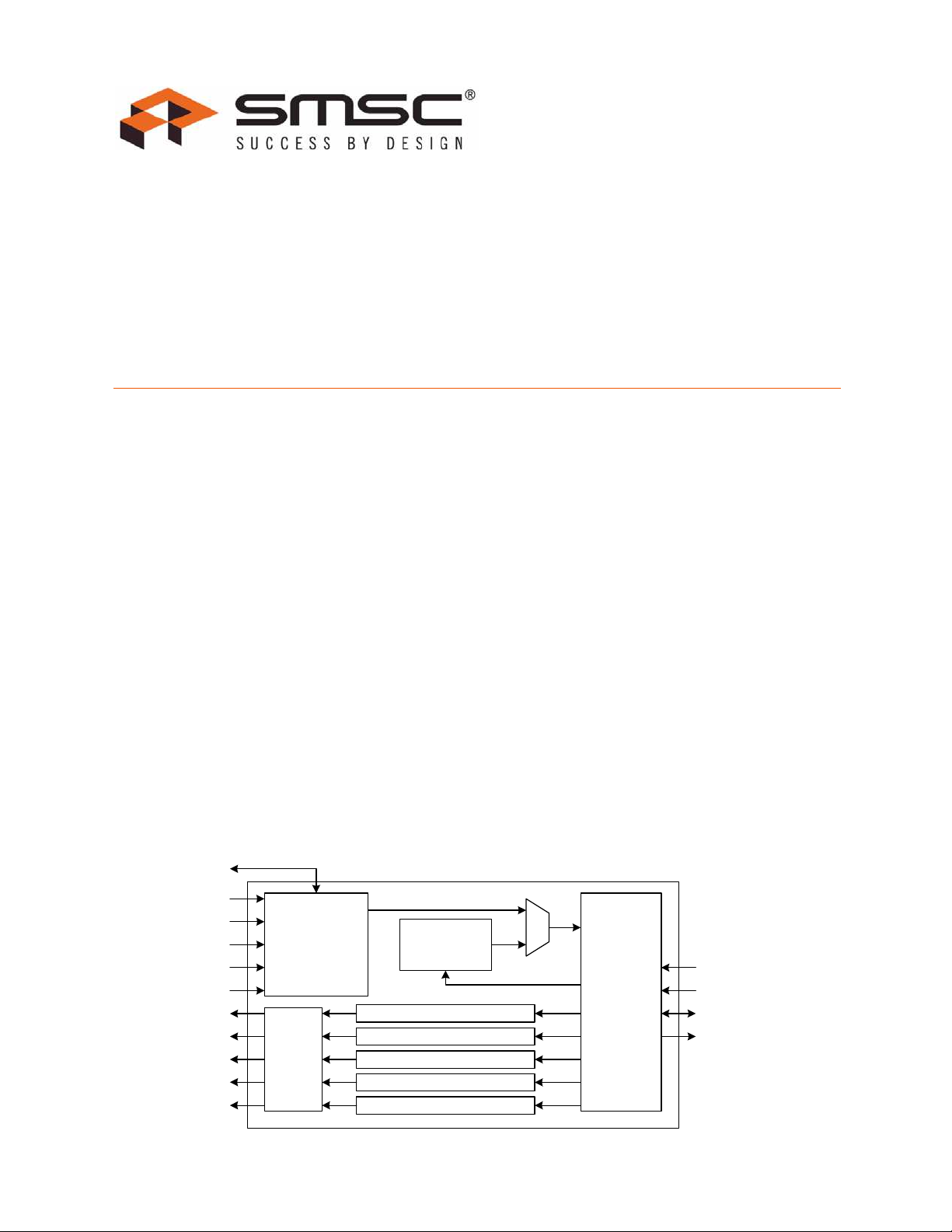
EMC2305
SMBus
Slave
Protocol
PWM
Drivers
SMCLK
SMDATA
Tachometer
Limit
Registers
PWM1
Tach
Measurement
TACH1
CLK
ADDR_SEL
ALERT#
PWM3
Fan Speed Control Algorithm
Fan Speed Control Algorithm
Fan Speed Control Algorithm
Fan Speed Control Algorithm
Fan Speed Control Algorithm
TACH2
TACH3
TACH4
PWM2
PWM4
PWM5
TACH5
Multiple RPM-Based PWM Fan Controller
for Five Fans
PRODUCT FEATURES
General Description
The EMC2305 is an SMBus compliant fan controller with
up to five independently controlled PWM fan drivers.
Each fan driver is controlled by a programmable
frequency PWM driver and Fan Speed Control algorithm
that operates in either a closed loop fashion or as a
directly PWM-controlled device.
The closed loop Fan Speed Control algorithm (FSC) has
the capability to detect aging fans and alert the system.
It will likewise detect stalled or locked fans and trigger
an interrupt.
Additionally, the EMC2305 offers a clock output so that
multiple devices may be chained and slaved to the
same clock source for optimal performance in large
distributed systems.
Applications
Servers
Projectors
Industrial and Networking Equipment
Notebook Computers
Datasheet
Features
Five Programmable Fan Control circuits (EMC2305)
— 4-wire fan compatible
— High speed PWM (26 kHz)
— Low speed PWM (9.5Hz - 2240 Hz)
— Optional detection of aging fans
— Fan Spin Up Control and Ramp Rate Control
— Alert on Fan Stall
— Up to 3 Selectable Default Fan Speeds
Watchdog Timer
RPM-based fan control algorithm
— 0.5% accuracy from 500 RPM to 16k RPM (external
crystal oscillator)
— 1% accuracy from 500 RPM to 16k RPM (internal clock)
SMBus 2.0 Compliant
— Up to 6 selectable SMBus addresses
— SMBus Alert compatible
CLK Pin can provide a clock source output
Available in a 16-pin 4mm x 4mm QFN Lead-free
RoHS Compliant package
Block Diagram
SMSC EMC2305 DATASHEET Revision 1.3 (05-18-11)
Page 2
Multiple RPM-Based PWM Fan Controller for Five Fans
Order Number:
ORDERING NUMBER PACKAGE FEATURES
Datasheet
EMC2305-1-AP-TR 16-pin QFN (Lead-free
RoHS compliant)
Five RPM-based fan speed control
algorithms
This product meets the halogen maximum concentration values per IEC 61249-2-21
For RoHS compliance and environmental information, please visit
www.smsc.com/rohs
80 ARKAY DRIVE, HAUPPAUGE, NY 11788 (631) 435-6000 or 1 (800) 443-SEMI
Copyright © 2011 SMSC or its subsidiaries. All rights reserved.
Circuit diagrams and other information relating to SMSC products are included as a mean s of illustrating typical applications. Conse quently, complete information sufficient for
construction purposes is not necessarily given. Although the information has been checked and is believed to be accurate, no responsibility is assumed for inaccuracies. SMSC
reserves the right to make changes to specifications and product descriptions at any time without notice. Contact your local SMSC sales office to obtain the latest specifications
before placing your product order. The provision of this information does not convey to the purchaser of the described semiconductor devices any licenses under any patent
rights or other intellectual property rights of SMSC or others. All sales are expressly conditional on your agreement to the terms and conditions of the most recently da ted
version of SMSC's standard Terms of Sale Agreement dated before the date of your order (the "Terms of Sale Agreement"). The product may contain design defects or errors
known as anomalies which may cause the product's functions to deviate from published specifications. Anomaly sheets are available upon request. SMSC products are not
designed, intended, authorized or warranted for use in any life support or other application where product failure could cause or contribute to personal injury or severe property
damage. Any and all such uses without prior written approval of an Officer of SMSC and further testing and/or modification will be fully at the risk of the customer. Copies of
this document or other SMSC literature, as well as the Terms of Sale Agreement, may be obtained by visiting SMSC’s website at http://www.smsc.com. SMSC is a registered
trademark of Standard Microsystems Corporation (“SMSC”). Product names and company names are the trademarks of their respective holders.
SMSC DISCLAIMS AND EXCLUDES ANY AND ALL WARRANTIES, INCLUDING WITHOUT LIMITATION ANY AND ALL IMPLIED WARRANTIES OF MERCHANTABILITY,
FITNESS FOR A PARTICULAR PURPOSE, TITLE, AND AGAINST INFRINGEMENT AND THE LIKE, AND ANY AND ALL WARRANTIES ARISING FROM ANY COURSE
OF DEALING OR USAGE OF TRADE. IN NO EVENT SHALL SMSC BE LIABLE FOR ANY DIRECT, INCIDENTAL, INDIRECT, SPECIAL, PUNITIVE, OR CONSEQUENTIAL
DAMAGES; OR FOR LOST DATA, PROFITS, SAVINGS OR REVENUES OF ANY KIND; REGARDLESS OF THE FORM OF ACTION, WHETHER BASED ON CONTRACT;
TORT; NEGLIGENCE OF SMSC OR OTHERS; STRICT LIABILITY; BREACH OF WARRANTY; OR OTHERWISE; WHETHER OR NOT ANY REMEDY OF BUYER IS HELD
TO HAVE FAILED OF ITS ESSENTIAL PURPOSE, AND WHETHER OR NOT SMSC HAS BEEN ADVISED OF THE POSSIBILITY OF SUCH DAMAGES.
Revision 1.3 (05-18-11) 2 SMSC EMC2305
DATASHEET
Page 3

Multiple RPM-Based PWM Fan Controller for Five Fans
Datasheet
Table of Contents
Chapter 1 Pin Description. . . . . . . . . . . . . . . . . . . . . . . . . . . . . . . . . . . . . . . . . . . . . . . . . . . . . 7
Chapter 2 Electrical Specifications . . . . . . . . . . . . . . . . . . . . . . . . . . . . . . . . . . . . . . . . . . . . 10
2.1 Electrical Specifications . . . . . . . . . . . . . . . . . . . . . . . . . . . . . . . . . . . . . . . . . . . . . . . . . . . . . . . . . 10
2.2 SMBus Electrical Specifications . . . . . . . . . . . . . . . . . . . . . . . . . . . . . . . . . . . . . . . . . . . . . . . . . . . 11
Chapter 3 Communications . . . . . . . . . . . . . . . . . . . . . . . . . . . . . . . . . . . . . . . . . . . . . . . . . . 13
3.1 System Management Bus Interface Protocol . . . . . . . . . . . . . . . . . . . . . . . . . . . . . . . . . . . . . . . . . 13
3.1.1 SMBus Start Bit . . . . . . . . . . . . . . . . . . . . . . . . . . . . . . . . . . . . . . . . . . . . . . . . . . . . . . . . 13
3.1.2 SMBus Address and RD / WR
3.1.3 SMBus Data Bytes . . . . . . . . . . . . . . . . . . . . . . . . . . . . . . . . . . . . . . . . . . . . . . . . . . . . . 14
3.1.4 SMBus ACK and NACK Bits . . . . . . . . . . . . . . . . . . . . . . . . . . . . . . . . . . . . . . . . . . . . . . 14
3.1.5 SMBus Stop Bit . . . . . . . . . . . . . . . . . . . . . . . . . . . . . . . . . . . . . . . . . . . . . . . . . . . . . . . . 14
3.1.6 SMBus Time-out . . . . . . . . . . . . . . . . . . . . . . . . . . . . . . . . . . . . . . . . . . . . . . . . . . . . . . . 14
3.1.7 SMBus and I
3.2 SMBus Protocols . . . . . . . . . . . . . . . . . . . . . . . . . . . . . . . . . . . . . . . . . . . . . . . . . . . . . . . . . . . . . . 15
3.2.1 Write Byte . . . . . . . . . . . . . . . . . . . . . . . . . . . . . . . . . . . . . . . . . . . . . . . . . . . . . . . . . . . . 15
3.2.2 Read Byte . . . . . . . . . . . . . . . . . . . . . . . . . . . . . . . . . . . . . . . . . . . . . . . . . . . . . . . . . . . . 15
3.2.3 Send Byte . . . . . . . . . . . . . . . . . . . . . . . . . . . . . . . . . . . . . . . . . . . . . . . . . . . . . . . . . . . . 15
3.2.4 Receive Byte . . . . . . . . . . . . . . . . . . . . . . . . . . . . . . . . . . . . . . . . . . . . . . . . . . . . . . . . . . 16
3.2.5 Block Write Protocol . . . . . . . . . . . . . . . . . . . . . . . . . . . . . . . . . . . . . . . . . . . . . . . . . . . . 16
3.2.6 Block Read Protocol . . . . . . . . . . . . . . . . . . . . . . . . . . . . . . . . . . . . . . . . . . . . . . . . . . . . 16
3.2.7 Alert Response Address . . . . . . . . . . . . . . . . . . . . . . . . . . . . . . . . . . . . . . . . . . . . . . . . . 16
2
C Compliance . . . . . . . . . . . . . . . . . . . . . . . . . . . . . . . . . . . . . . . . . . . . . . 14
Bit . . . . . . . . . . . . . . . . . . . . . . . . . . . . . . . . . . . . . . . . . . 13
Chapter 4 Product Description. . . . . . . . . . . . . . . . . . . . . . . . . . . . . . . . . . . . . . . . . . . . . . . . 18
4.1 Fan Control Modes of Operation . . . . . . . . . . . . . . . . . . . . . . . . . . . . . . . . . . . . . . . . . . . . . . . . . . 18
4.2 PWM Fan Driver . . . . . . . . . . . . . . . . . . . . . . . . . . . . . . . . . . . . . . . . . . . . . . . . . . . . . . . . . . . . . . . 19
4.3 RPM-based Fan Speed Control Algorithm (FSC). . . . . . . . . . . . . . . . . . . . . . . . . . . . . . . . . . . . . . 19
4.3.1 Programming the RPM-based Fan Speed Control Algorithm . . . . . . . . . . . . . . . . . . . . . 20
4.4 Tachometer Measurement . . . . . . . . . . . . . . . . . . . . . . . . . . . . . . . . . . . . . . . . . . . . . . . . . . . . . . . 20
4.4.1 Stalled Fan . . . . . . . . . . . . . . . . . . . . . . . . . . . . . . . . . . . . . . . . . . . . . . . . . . . . . . . . . . . 21
4.4.2 Aging Fan or Invalid Drive Detection. . . . . . . . . . . . . . . . . . . . . . . . . . . . . . . . . . . . . . . . 21
4.5 CLK Pin. . . . . . . . . . . . . . . . . . . . . . . . . . . . . . . . . . . . . . . . . . . . . . . . . . . . . . . . . . . . . . . . . . . . . . 21
4.5.1 Pull Up Decode . . . . . . . . . . . . . . . . . . . . . . . . . . . . . . . . . . . . . . . . . . . . . . . . . . . . . . . . 21
4.5.2 External Clock . . . . . . . . . . . . . . . . . . . . . . . . . . . . . . . . . . . . . . . . . . . . . . . . . . . . . . . . . 22
4.5.3 Internal Clock. . . . . . . . . . . . . . . . . . . . . . . . . . . . . . . . . . . . . . . . . . . . . . . . . . . . . . . . . . 22
4.6 Spin Up Routine . . . . . . . . . . . . . . . . . . . . . . . . . . . . . . . . . . . . . . . . . . . . . . . . . . . . . . . . . . . . . . . 22
4.6.1 Power Up Options . . . . . . . . . . . . . . . . . . . . . . . . . . . . . . . . . . . . . . . . . . . . . . . . . . . . . . 23
4.7 Ramp Rate Control. . . . . . . . . . . . . . . . . . . . . . . . . . . . . . . . . . . . . . . . . . . . . . . . . . . . . . . . . . . . . 23
4.8 Watchdog Timer . . . . . . . . . . . . . . . . . . . . . . . . . . . . . . . . . . . . . . . . . . . . . . . . . . . . . . . . . . . . . . . 24
4.8.1 Power Up Operation . . . . . . . . . . . . . . . . . . . . . . . . . . . . . . . . . . . . . . . . . . . . . . . . . . . . 24
4.8.2 Continuous Operation . . . . . . . . . . . . . . . . . . . . . . . . . . . . . . . . . . . . . . . . . . . . . . . . . . . 25
Chapter 5 Register Set. . . . . . . . . . . . . . . . . . . . . . . . . . . . . . . . . . . . . . . . . . . . . . . . . . . . . . . 26
5.1 Register Map . . . . . . . . . . . . . . . . . . . . . . . . . . . . . . . . . . . . . . . . . . . . . . . . . . . . . . . . . . . . . . . . . 26
5.1.1 Lock Entries. . . . . . . . . . . . . . . . . . . . . . . . . . . . . . . . . . . . . . . . . . . . . . . . . . . . . . . . . . . 31
5.2 Configuration Register . . . . . . . . . . . . . . . . . . . . . . . . . . . . . . . . . . . . . . . . . . . . . . . . . . . . . . . . . . 31
5.3 Fan Status Registers . . . . . . . . . . . . . . . . . . . . . . . . . . . . . . . . . . . . . . . . . . . . . . . . . . . . . . . . . . . 32
5.3.1 Fan Status - 24h . . . . . . . . . . . . . . . . . . . . . . . . . . . . . . . . . . . . . . . . . . . . . . . . . . . . . . . 32
5.3.2 Fan Stall Status - 25h . . . . . . . . . . . . . . . . . . . . . . . . . . . . . . . . . . . . . . . . . . . . . . . . . . . 33
SMSC EMC2305 3 Revision 1.3 (05-18-11)
DATASHEET
Page 4

Multiple RPM-Based PWM Fan Controller for Five Fans
Datasheet
5.3.3 Fan Spin Status - 26h . . . . . . . . . . . . . . . . . . . . . . . . . . . . . . . . . . . . . . . . . . . . . . . . . . . 33
5.3.4 Fan Drive Fail Status - 27h . . . . . . . . . . . . . . . . . . . . . . . . . . . . . . . . . . . . . . . . . . . . . . . 33
5.4 Fan Interrupt Enable Register. . . . . . . . . . . . . . . . . . . . . . . . . . . . . . . . . . . . . . . . . . . . . . . . . . . . . 33
5.5 PWM Configuration Registers . . . . . . . . . . . . . . . . . . . . . . . . . . . . . . . . . . . . . . . . . . . . . . . . . . . . 34
5.5.1 PWM Polarity Config - 2Ah . . . . . . . . . . . . . . . . . . . . . . . . . . . . . . . . . . . . . . . . . . . . . . . 34
5.5.2 PWM Output Config - 2Bh. . . . . . . . . . . . . . . . . . . . . . . . . . . . . . . . . . . . . . . . . . . . . . . . 34
5.6 PWM Base Frequency Registers . . . . . . . . . . . . . . . . . . . . . . . . . . . . . . . . . . . . . . . . . . . . . . . . . . 35
5.6.1 PWM Base Frequency 1 - 2Bh . . . . . . . . . . . . . . . . . . . . . . . . . . . . . . . . . . . . . . . . . . . . 35
5.6.2 PWM Base Frequency 2 - 2Ch . . . . . . . . . . . . . . . . . . . . . . . . . . . . . . . . . . . . . . . . . . . . 35
5.7 Fan Setting Registers. . . . . . . . . . . . . . . . . . . . . . . . . . . . . . . . . . . . . . . . . . . . . . . . . . . . . . . . . . . 36
5.8 PWM Divide Registers . . . . . . . . . . . . . . . . . . . . . . . . . . . . . . . . . . . . . . . . . . . . . . . . . . . . . . . . . . 36
5.9 Fan Configuration 1 Registers . . . . . . . . . . . . . . . . . . . . . . . . . . . . . . . . . . . . . . . . . . . . . . . . . . . . 37
5.10 Fan Configuration 2 Registers . . . . . . . . . . . . . . . . . . . . . . . . . . . . . . . . . . . . . . . . . . . . . . . . . . . . 38
5.11 Gain Registers . . . . . . . . . . . . . . . . . . . . . . . . . . . . . . . . . . . . . . . . . . . . . . . . . . . . . . . . . . . . . . . . 40
5.12 Fan Spin Up Configuration Registers . . . . . . . . . . . . . . . . . . . . . . . . . . . . . . . . . . . . . . . . . . . . . . . 41
5.13 Fan Max Step Registers. . . . . . . . . . . . . . . . . . . . . . . . . . . . . . . . . . . . . . . . . . . . . . . . . . . . . . . . . 43
5.14 Fan Minimum Drive Registers . . . . . . . . . . . . . . . . . . . . . . . . . . . . . . . . . . . . . . . . . . . . . . . . . . . . 44
5.15 Valid TACH Count Registers . . . . . . . . . . . . . . . . . . . . . . . . . . . . . . . . . . . . . . . . . . . . . . . . . . . . . 44
5.16 Fan Drive Fail Band Registers . . . . . . . . . . . . . . . . . . . . . . . . . . . . . . . . . . . . . . . . . . . . . . . . . . . . 45
5.17 TACH Target Registers . . . . . . . . . . . . . . . . . . . . . . . . . . . . . . . . . . . . . . . . . . . . . . . . . . . . . . . . . 46
5.18 TACH Reading Registers . . . . . . . . . . . . . . . . . . . . . . . . . . . . . . . . . . . . . . . . . . . . . . . . . . . . . . . . 47
5.19 Software Lock Register. . . . . . . . . . . . . . . . . . . . . . . . . . . . . . . . . . . . . . . . . . . . . . . . . . . . . . . . . . 48
5.20 Product Features Register . . . . . . . . . . . . . . . . . . . . . . . . . . . . . . . . . . . . . . . . . . . . . . . . . . . . . . . 48
5.21 Product ID Register . . . . . . . . . . . . . . . . . . . . . . . . . . . . . . . . . . . . . . . . . . . . . . . . . . . . . . . . . . . . 49
5.22 Manufacturer ID Register . . . . . . . . . . . . . . . . . . . . . . . . . . . . . . . . . . . . . . . . . . . . . . . . . . . . . . . . 50
5.23 Revision Register . . . . . . . . . . . . . . . . . . . . . . . . . . . . . . . . . . . . . . . . . . . . . . . . . . . . . . . . . . . . . . 50
Chapter 6 Typical Operating Curves. . . . . . . . . . . . . . . . . . . . . . . . . . . . . . . . . . . . . . . . . . . 51
Chapter 7 Package Drawing . . . . . . . . . . . . . . . . . . . . . . . . . . . . . . . . . . . . . . . . . . . . . . . . . . 53
7.1 EMC2305 Package Information . . . . . . . . . . . . . . . . . . . . . . . . . . . . . . . . . . . . . . . . . . . . . . . . . . . 53
7.2 Package Markings . . . . . . . . . . . . . . . . . . . . . . . . . . . . . . . . . . . . . . . . . . . . . . . . . . . . . . . . . . . . . 55
Chapter 8 Datasheet Revision History. . . . . . . . . . . . . . . . . . . . . . . . . . . . . . . . . . . . . . . . . . 56
Revision 1.3 (05-18-11) 4 SMSC EMC2305
DATASHEET
Page 5

Multiple RPM-Based PWM Fan Controller for Five Fans
Datasheet
List of Figures
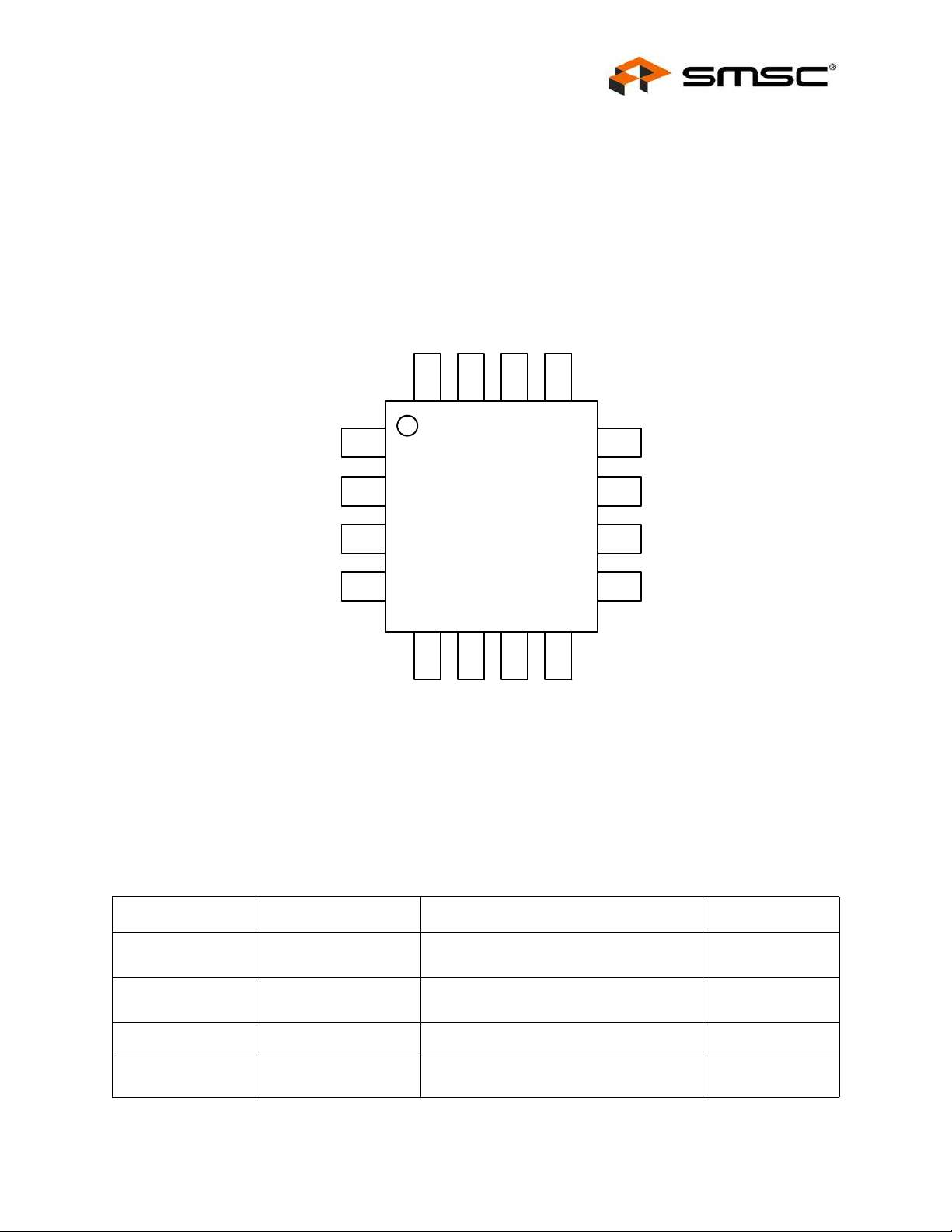
Figure 1.1 EMC2305 Pin Diagram (16-Pin QFN) . . . . . . . . . . . . . . . . . . . . . . . . . . . . . . . . . . . . . . . . . . . 7
Figure 3.1 SMBus Timing Diagram. . . . . . . . . . . . . . . . . . . . . . . . . . . . . . . . . . . . . . . . . . . . . . . . . . . . . 13
Figure 4.1 System Diagram of EMC2305 . . . . . . . . . . . . . . . . . . . . . . . . . . . . . . . . . . . . . . . . . . . . . . . . 18
Figure 4.2 Spin Up Routine. . . . . . . . . . . . . . . . . . . . . . . . . . . . . . . . . . . . . . . . . . . . . . . . . . . . . . . . . . . 23
Figure 4.3 Ramp Rate Control . . . . . . . . . . . . . . . . . . . . . . . . . . . . . . . . . . . . . . . . . . . . . . . . . . . . . . . . 24
Figure 7.1 Package Drawing - 16-Pin QFN 4mm x 4mm . . . . . . . . . . . . . . . . . . . . . . . . . . . . . . . . . . . . 53
Figure 7.2 Package Dimensions - 16-Pin QFN 4mm x 4mm . . . . . . . . . . . . . . . . . . . . . . . . . . . . . . . . . 54
Figure 7.3 PCB Footprint - 16-Pin QFN 4mm x 4mm . . . . . . . . . . . . . . . . . . . . . . . . . . . . . . . . . . . . . . . 54
Figure 7.4 EMC2305 Package Markings. . . . . . . . . . . . . . . . . . . . . . . . . . . . . . . . . . . . . . . . . . . . . . . . . 55
SMSC EMC2305 5 Revision 1.3 (05-18-11)
DATASHEET
Page 6

Multiple RPM-Based PWM Fan Controller for Five Fans
Datasheet
List of Tables
Table 1.1 Pin Description for EMC2305 . . . . . . . . . . . . . . . . . . . . . . . . . . . . . . . . . . . . . . . . . . . . . . . . . . 7
Table 1.2 Pin Types. . . . . . . . . . . . . . . . . . . . . . . . . . . . . . . . . . . . . . . . . . . . . . . . . . . . . . . . . . . . . . . . . . 9
Table 2.1 Absolute Maximum Ratings. . . . . . . . . . . . . . . . . . . . . . . . . . . . . . . . . . . . . . . . . . . . . . . . . . . 10
Table 2.2 Electrical Specifications. . . . . . . . . . . . . . . . . . . . . . . . . . . . . . . . . . . . . . . . . . . . . . . . . . . . . . 10
Table 2.3 SMBus Electrical Specifications . . . . . . . . . . . . . . . . . . . . . . . . . . . . . . . . . . . . . . . . . . . . . . . 11
Table 3.1 ADDR_SEL Pin Decode . . . . . . . . . . . . . . . . . . . . . . . . . . . . . . . . . . . . . . . . . . . . . . . . . . . . . 14
Table 3.2 Protocol Format . . . . . . . . . . . . . . . . . . . . . . . . . . . . . . . . . . . . . . . . . . . . . . . . . . . . . . . . . . . . 15
Table 3.3 Write Byte Protocol . . . . . . . . . . . . . . . . . . . . . . . . . . . . . . . . . . . . . . . . . . . . . . . . . . . . . . . . . 15
Table 3.4 Read Byte Protocol . . . . . . . . . . . . . . . . . . . . . . . . . . . . . . . . . . . . . . . . . . . . . . . . . . . . . . . . . 15
Table 3.5 Send Byte Protocol . . . . . . . . . . . . . . . . . . . . . . . . . . . . . . . . . . . . . . . . . . . . . . . . . . . . . . . . . 15
Table 3.6 Receive Byte Protocol . . . . . . . . . . . . . . . . . . . . . . . . . . . . . . . . . . . . . . . . . . . . . . . . . . . . . . . 16
Table 3.7 Block Write Protocol . . . . . . . . . . . . . . . . . . . . . . . . . . . . . . . . . . . . . . . . . . . . . . . . . . . . . . . . 16
Table 3.8 Block Read Protocol . . . . . . . . . . . . . . . . . . . . . . . . . . . . . . . . . . . . . . . . . . . . . . . . . . . . . . . . 16
Table 3.9 Alert Response Address Protocol . . . . . . . . . . . . . . . . . . . . . . . . . . . . . . . . . . . . . . . . . . . . . . 17
Table 4.1 Fan Controls Active for Operating Mode . . . . . . . . . . . . . . . . . . . . . . . . . . . . . . . . . . . . . . . . . 19
Table 4.2 CLK Pin Pull-Up Decode . . . . . . . . . . . . . . . . . . . . . . . . . . . . . . . . . . . . . . . . . . . . . . . . . . . . . 21
Table 5.1 EMC2305 Register Set . . . . . . . . . . . . . . . . . . . . . . . . . . . . . . . . . . . . . . . . . . . . . . . . . . . . . . 26
Table 5.2 Configuration Register. . . . . . . . . . . . . . . . . . . . . . . . . . . . . . . . . . . . . . . . . . . . . . . . . . . . . . . 31
Table 5.3 Fan Status Registers . . . . . . . . . . . . . . . . . . . . . . . . . . . . . . . . . . . . . . . . . . . . . . . . . . . . . . . . 32
Table 5.4 Fan Interrupt Enable Register . . . . . . . . . . . . . . . . . . . . . . . . . . . . . . . . . . . . . . . . . . . . . . . . . 33
Table 5.5 PWM Configuration Registers . . . . . . . . . . . . . . . . . . . . . . . . . . . . . . . . . . . . . . . . . . . . . . . . . 34
Table 5.6 PWM Base Frequency Registers. . . . . . . . . . . . . . . . . . . . . . . . . . . . . . . . . . . . . . . . . . . . . . . 35
Table 5.7 PWM_BASEx[1:0] Bit Decode. . . . . . . . . . . . . . . . . . . . . . . . . . . . . . . . . . . . . . . . . . . . . . . . . 35
Table 5.8 Fan Driver Setting Registers . . . . . . . . . . . . . . . . . . . . . . . . . . . . . . . . . . . . . . . . . . . . . . . . . . 36
Table 5.9 PWM Divide Registers. . . . . . . . . . . . . . . . . . . . . . . . . . . . . . . . . . . . . . . . . . . . . . . . . . . . . . . 36
Table 5.10 Fan Configuration 1 Registers. . . . . . . . . . . . . . . . . . . . . . . . . . . . . . . . . . . . . . . . . . . . . . . . . 37
Table 5.11 Range Decode. . . . . . . . . . . . . . . . . . . . . . . . . . . . . . . . . . . . . . . . . . . . . . . . . . . . . . . . . . . . . 37
Table 5.12 Minimum Edges for Fan Rotation . . . . . . . . . . . . . . . . . . . . . . . . . . . . . . . . . . . . . . . . . . . . . . 38
Table 5.13 Update Time . . . . . . . . . . . . . . . . . . . . . . . . . . . . . . . . . . . . . . . . . . . . . . . . . . . . . . . . . . . . . . 38
Table 5.14 Fan Configuration 2 Registers. . . . . . . . . . . . . . . . . . . . . . . . . . . . . . . . . . . . . . . . . . . . . . . . . 38
Table 5.15 Derivative Options . . . . . . . . . . . . . . . . . . . . . . . . . . . . . . . . . . . . . . . . . . . . . . . . . . . . . . . . . . 39
Table 5.16 Error Range Options . . . . . . . . . . . . . . . . . . . . . . . . . . . . . . . . . . . . . . . . . . . . . . . . . . . . . . . . 40
Table 5.17 Gain Registers. . . . . . . . . . . . . . . . . . . . . . . . . . . . . . . . . . . . . . . . . . . . . . . . . . . . . . . . . . . . . 40
Table 5.18 Gain Decode . . . . . . . . . . . . . . . . . . . . . . . . . . . . . . . . . . . . . . . . . . . . . . . . . . . . . . . . . . . . . . 41
Table 5.19 Fan Spin Up Configuration Registers . . . . . . . . . . . . . . . . . . . . . . . . . . . . . . . . . . . . . . . . . . . 41
Table 5.20 DRIVE_FAIL_CNT[1:0] Bit Decode . . . . . . . . . . . . . . . . . . . . . . . . . . . . . . . . . . . . . . . . . . . . . 41
Table 5.21 Spin Level . . . . . . . . . . . . . . . . . . . . . . . . . . . . . . . . . . . . . . . . . . . . . . . . . . . . . . . . . . . . . . . . 42
Table 5.22 Spin Time. . . . . . . . . . . . . . . . . . . . . . . . . . . . . . . . . . . . . . . . . . . . . . . . . . . . . . . . . . . . . . . . . 43
Table 5.23 Fan Max Step Registers . . . . . . . . . . . . . . . . . . . . . . . . . . . . . . . . . . . . . . . . . . . . . . . . . . . . . 43
Table 5.24Minimum Fan Drive Registers . . . . . . . . . . . . . . . . . . . . . . . . . . . . . . . . . . . . . . . . . . . . . . . . . 44
Table 5.25 Valid TACH Count Registers. . . . . . . . . . . . . . . . . . . . . . . . . . . . . . . . . . . . . . . . . . . . . . . . . . 44
Table 5.26 Fan Drive Fail Band Registers. . . . . . . . . . . . . . . . . . . . . . . . . . . . . . . . . . . . . . . . . . . . . . . . . 45
Table 5.27 TACH Target Registers . . . . . . . . . . . . . . . . . . . . . . . . . . . . . . . . . . . . . . . . . . . . . . . . . . . . . . 46
Table 5.28 TACH Reading Registers . . . . . . . . . . . . . . . . . . . . . . . . . . . . . . . . . . . . . . . . . . . . . . . . . . . . 47
Table 5.29 Software Lock Register . . . . . . . . . . . . . . . . . . . . . . . . . . . . . . . . . . . . . . . . . . . . . . . . . . . . . . 48
Table 5.30 Product Features Register. . . . . . . . . . . . . . . . . . . . . . . . . . . . . . . . . . . . . . . . . . . . . . . . . . . . 48
Table 5.31 ADDR_SEL Pin Configuration. . . . . . . . . . . . . . . . . . . . . . . . . . . . . . . . . . . . . . . . . . . . . .
Table 5.32 FAN_SPD Pin Configuration . . . . . . . . . . . . . . . . . . . . . . . . . . . . . . . . . . . . . . . . . . . . . . . . . . 49
Table 5.33 Product ID Register . . . . . . . . . . . . . . . . . . . . . . . . . . . . . . . . . . . . . . . . . . . . . . . . . . . . . . . . . 49
Table 5.34 Manufacturer ID Register. . . . . . . . . . . . . . . . . . . . . . . . . . . . . . . . . . . . . . . . . . . . . . . . . . . . . 50
Table 5.35 Revision Register. . . . . . . . . . . . . . . . . . . . . . . . . . . . . . . . . . . . . . . . . . . . . . . . . . . . . . . . . . . 50
Table 8.1 Customer Revision History . . . . . . . . . . . . . . . . . . . . . . . . . . . . . . . . . . . . . . . . . . . . . . . . . . . 56
. . . 49
Revision 1.3 (05-18-11) 6 SMSC EMC2305
DATASHEET
Page 7
Multiple RPM-Based PWM Fan Controller for Five Fans
EMC2305
16-QFN
1
2
3
4
5
6
7
8
12
11
10
9
16
15
14
13
VDD
SMCLK
PWM1
TACH2
SMDATA
CLK
ADDR_SEL
TACH1
PWM2
PWM 3
TACH3
ALERT#
PWM4
TACH4
TACH5
PWM5
Datasheet
Chapter 1 Pin Description
PIN NUMBER PIN NAME PIN FUNCTION PIN TYPE
1SMDATA
2SMCLK
3 VDD Power Supply Power
4 ADDR_SEL
SMSC EMC2305 7 Revision 1.3 (05-18-11)
Figure 1.1 EMC2305 Pin Diag ram (16-Pin QFN)
Ta bl e 1.1 Pin Description for EMC2305
SMBus data input/output - requires
external pull-up resistor
SMBus clock input - requires external
pull-up resistor
Address selection input - requires pull-up
resistor
DATASHEET
DIOD (5V)
DI (5V)
AIO
Page 8

Multiple RPM-Based PWM Fan Controller for Five Fans
Datasheet
Table 1.1 Pin Description for EMC2305 (continued)
PIN NUMBER PIN NAME PIN FUNCTION PIN TYPE
5PWM1
Push-Pull PWM output driver for Fan 1 DO
Open Drain PWM output driver for Fan 1 OD (5V)
6TACH1
Open drain tachometer input for Fan 1-
Push-Pull PWM output driver for Fan 2 DO
7PWM2
Open Drain PWM output driver for Fan 2 OD (5V)
8TACH2
Open drain tachometer input for Fan 2 -
Push-Pull PWM output driver for Fan 3 DO
9PWM3
Open Drain PWM output driver for Fan 3 OD (5V)
10 TACH3
Open drain tachometer input for Fan 3 -
Clock input for tachometer measurement DI (5V)
11 CLK
Push Pull Clock output to other fan
controllers to synchronize Fan Speed
12 ALERT#
Active low interrupt - requires external
Push-Pull PWM output driver for Fan 4 DO
13 PWM4
Open Drain PWM output driver for Fan 4 OD (5V)
requires pull-up resistor
requires pull-up resistor
requires pull-up resistor
Control
pull-up resistor.
DI (5V)
DI (5V)
DI (5V)
DO
OD (5V)
14 TACH4
Open drain tachometer input for Fan 4 -
requires pull-up resistor
DI (5V)
Push-Pull PWM output driver for Fan 5 DO
15 PWM5
Open Drain PWM output driver for Fan 5 OD (5V)
16 TACH5
Open drain tachometer input for Fan 5 -
requires pull-up resistor
DI (5V)
Bottom Pad GND Ground Powe r
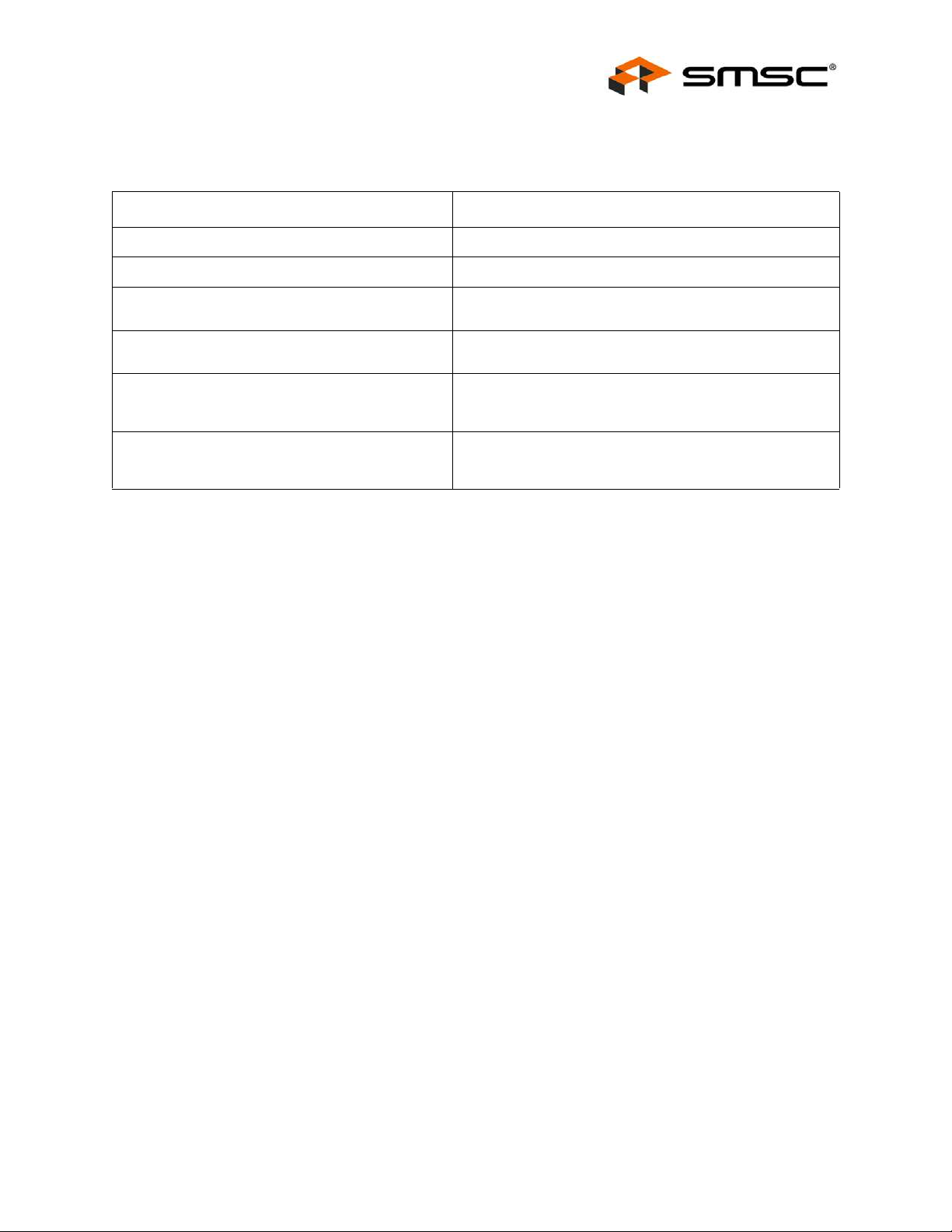
The pin types are described in detail below. All pins labeled with (5V) are 5V tolerant.
APPLICATION NOTE: For the 5V tolerant pins that have a pull-up resistor, the voltage difference between VDD and
the 5V tolerant pad must never be more than 3.6V.
Revision 1.3 (05-18-11) 8 SMSC EMC2305
DATASHEET
Page 9
Multiple RPM-Based PWM Fan Controller for Five Fans
Datasheet
PIN TYPE DESCRIPTION
Power This pin is used to supply power or ground to the device.
AIO Analog input / output - this pin is used for analog signals
Table 1.2 Pin Types
DI
DO
DIOD
OD
Digital Input - this pin is used as a digital input. This pin is
5V tolerant.
Push / Pull Digital Output - this pin is used as a digital
output. It can both source and sink current.
Digital Input / Open Drain Output this pin is used as a
digital I/O. When it is used as an output, it is open drain
and requires a pull-up resistor. This pin is 5V tolerant.
Open Drain Digital Output - this pin is used as a digital
output. It is open drain and requires a pull-up resistor. This
pin is 5V tolerant.
SMSC EMC2305 9 Revision 1.3 (05-18-11)
DATASHEET
Page 10
Multiple RPM-Based PWM Fan Controller for Five Fans
Chapter 2 Electrical Specifications
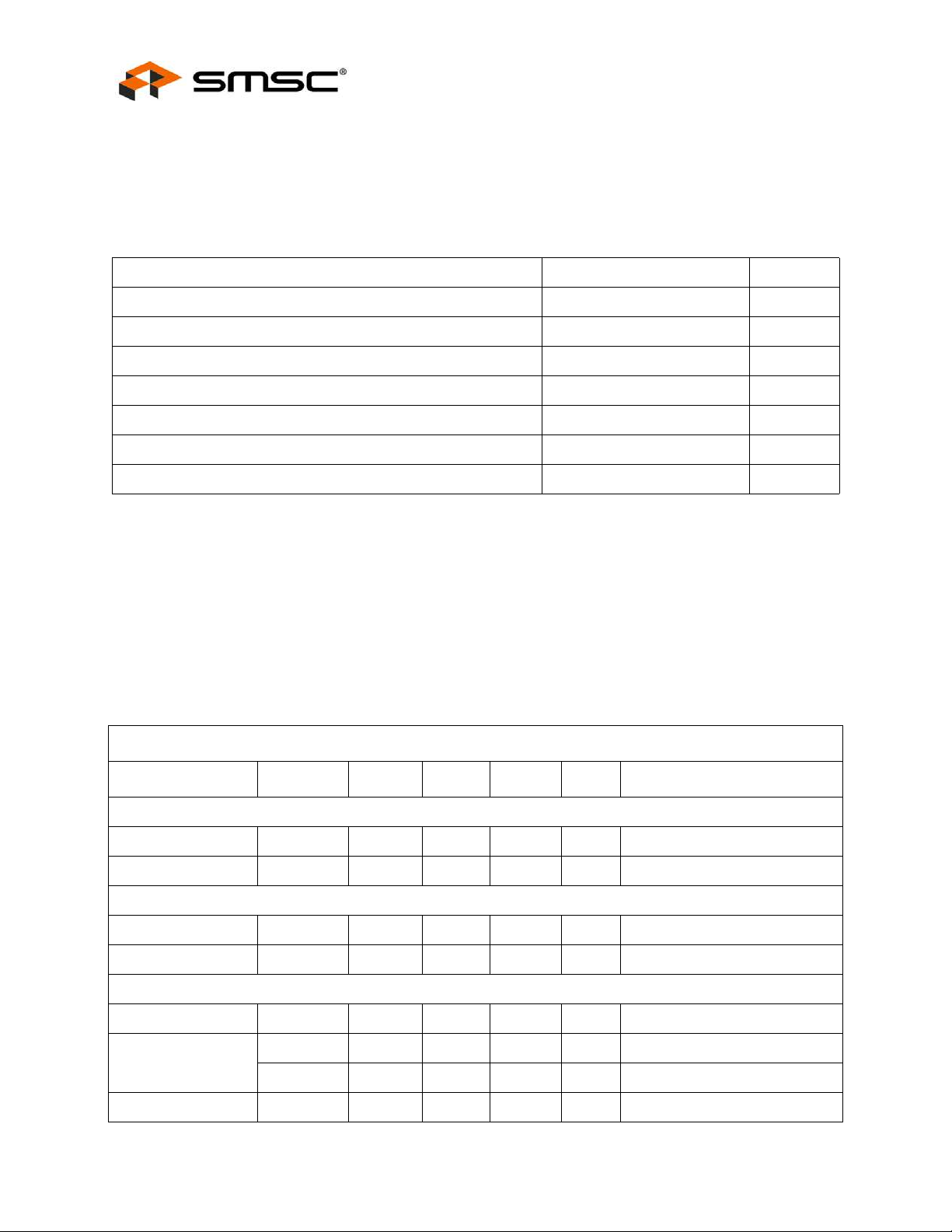
Table 2.1 Absolute Maximum Ratings
Datasheet
Voltage on 5V tolerant pins (V
Voltage on 5V tolerant pins (|V
) -0.3 to 5.5 V
5VT_pin
5VT_pin
- VDD|) (see
Note 2.1)0 to 3.6 V
Voltage on VDD pin -0.3 to 4 V
Voltage on any other pin to GND -0.3 to VDD + 0.3 V
Package Thermal Resistance - Junction to Ambient (θ
)40 °C/W
JA
Operating Ambient Temperature Range -40 to 125 °C
Storage Temperature Range -55 to 150 °C
ESD Rating, All Pins, HBM 2000 V
Note: Stresses above those listed could cause permanent damage to the device. This is a stress
rating only and functional operation of the device at any other conditio n above those indicated
in the operation sections of this specification is not implied.
Note 2.1 For the 5V tolerant pins that have a pull-up resistor, the pull-up voltage must not exceed
3.6V when the EMC2305 is unpowered.
2.1 Electrical Specifications
Table 2.2 Electrical Specifications
V
= 3V to 3.6V, TA = -40°C to 125°C, all Typical values at TA = 27°C unless otherwise noted.
DD
CHARACTERISTIC SYMBOL MIN TYP M AX UNIT CONDITIONS
DC Power
Supply Voltage V
Supply Current I
DD
DD
33.33.6V
625 800 uA
PWM Fan Driver
PWM Resolution PWM 256 Steps
PWM Duty Cycle DUTY 0 100 %
RPM-based Fan Controller
Tachometer Range TACH 480 16000 RPM
Tachometer Setting
Accuracy
Input High Voltage V
Revision 1.3 (05-18-11) 10 SMSC EMC2305
Δ
Δ
TACH
TACH
IH
±0.5 ±1 % External oscillator 32.768kHz
±1 ±2 % Internal Oscillator
2.0 V
DATASHEET
Page 11
Multiple RPM-Based PWM Fan Controller for Five Fans
Datasheet
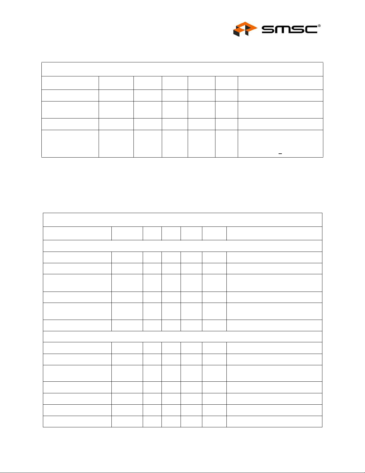
Table 2.2 Electrical Specifications (continued)
VDD = 3V to 3.6V, TA = -40°C to 125°C, all Typical values at TA = 27°C unless otherwise noted.
CHARACTERISTIC SYMBOL MIN TYP M AX UNIT CONDITIONS
Input Low Voltage V
Output High Voltage
Output Low Voltage V
Leakage current
I
IL
V
OH
OL
LEAK
VDD -
0.4
0.8 V
8 mA current drive
V
0.4 V 8 mA current sink
ALERT# pin
±5 uA
Powered and unpowered
0°C < TA < 85°C
pull-up voltage <
Note 2.2 All voltages are relative to ground.
2.2 SMBus Electrical Specifications
Table 2.3 SMBus Ele ctrical Specifications
VDD= 3V to 3.6V, T
CHARACTERISTIC SYMBOL MIN TYP MAX UNITS CONDITIONS
Input High Voltage V
Input Low Voltage V
Output High Voltage
= -40°C to 125°C Typical values are at TA = 27°C unless otherwise noted.
A
SMBus Interface
IH
IL
V
OH
2.0 V
0.8 V
VDD
- 0.4
V
3.6V
Output Low Voltage V
Input High/Low Current
I
IH / IIL
Input Capacitance C
OL
IN
5pF
0.4 V 4 mA current sink
±5 uA
Powered and unpowered
0°C < TA < 85°C
SMBus Timing
Clock Frequency f
Spike Suppression t
Bus free time Start to
Sto p
Setup Time: Start t
Setup Time: Stop t
Data Hold Time t
Data Setup Time t
SMSC EMC2305 11 Revision 1.3 (05-18-11)
SMB
SP
t
BUF
SU:STA
SU:STP
HD:DAT
SU:DAT
10 400 kHz
50 ns
1.3 us
0.6 us
0.6 us
0us
0.6 us
DATASHEET
Page 12
Multiple RPM-Based PWM Fan Controller for Five Fans
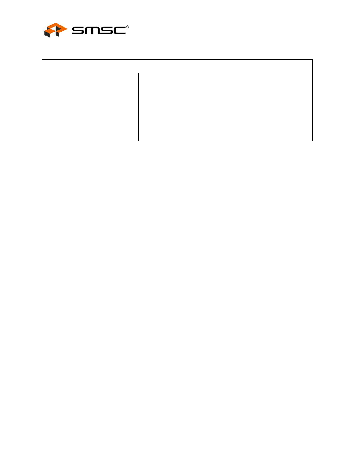
T able 2.3 SMBus Electrical Specifications (continued)
Datasheet
VDD= 3V to 3.6V, T
= -40°C to 125°C Typical values are at TA = 27°C unless otherwise noted.
A
CHARACTERISTIC SYMBOL MIN TYP MAX UNITS CONDITIONS
Clock Low Period t
Clock High Period t
Clock/Data Fall time t
Clock/Data Rise time t
Capacitive Load C
LOW
HIGH
FAL L
RISE
LOAD
1.3 us
0.6 us
300 ns Min = 20+0.1C
300 ns Min = 20+0.1C
400 pF per bus line
LOAD
LOAD
ns
ns
Revision 1.3 (05-18-11) 12 SMSC EMC2305
DATASHEET
Page 13
Multiple RPM-Based PWM Fan Controller for Five Fans
SMDATA
SMCLK
T
LOW
T
RISE
T
HIGH
T
FALL
T
BUF
T
HD:STA
P
S
S - Start Condition
P - Stop Condition
T
HD:DAT
T
SU:DAT
T
SU:STA
T
HD:STA
P
T
SU:STO
S
Datasheet
Chapter 3 Communications
3.1 System Management Bus Interface Protocol
The EMC2305 communicates with a host controller, such as an SMSC SIO, through the SMBus. The
SMBus is a two-wire serial communication protocol between a computer host and its peripheral
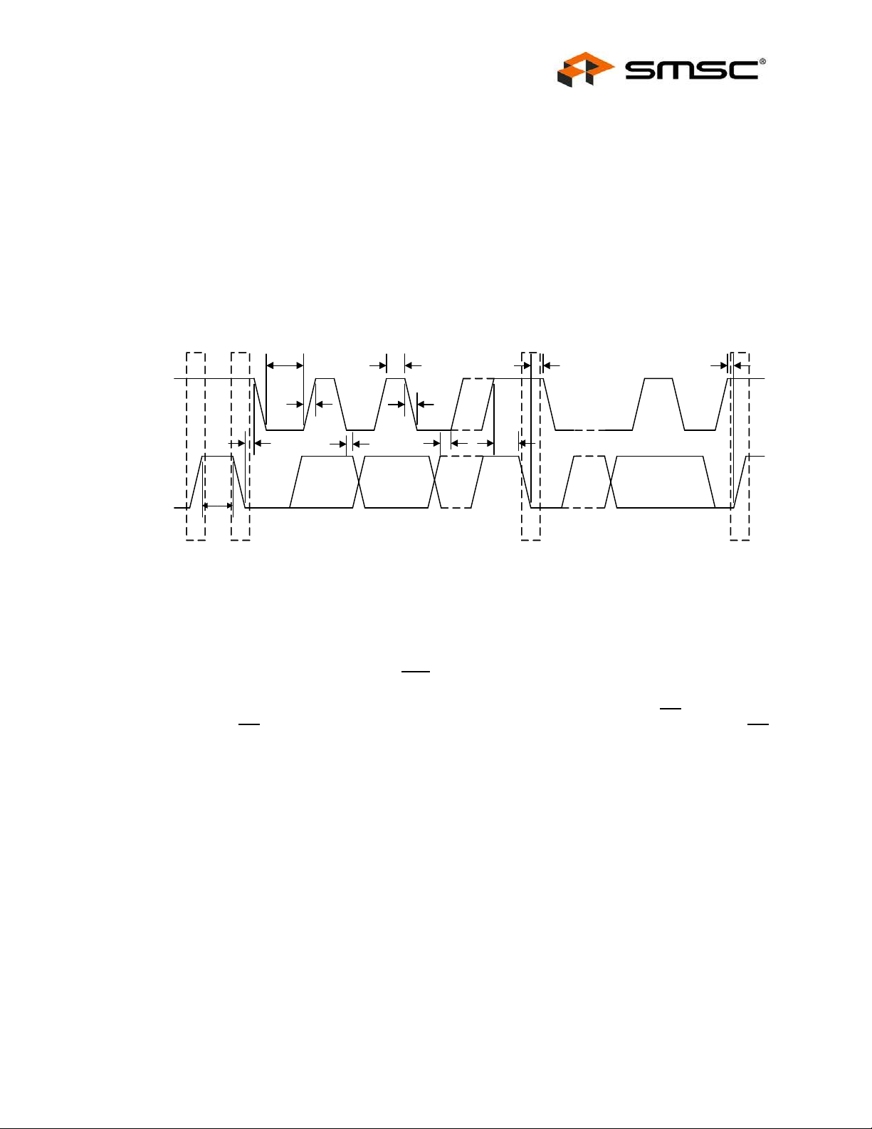
devices. A detailed timing diagram is shown in
however, the EMC2305 will not stretch the clock signal.
Figure 3.1. Stretching of the SMCLK signal is supported;
Figure 3.1 SMBus Timing Diagram
3.1.1 SMBus Start Bit
The SMBus Start bit is defined as a transition of the SMBus Data line from a logic ‘1’ state to a logic
‘0’ state while the SMBus Clock line is in a logic ‘1’ state.
3.1.2 SMBus Address and RD / WR Bit
The SMBus Address Byte consists of the 7-bit client address followed by a RD / WR
this RD / WR
bit is a logic ‘1’, then the SMBus Host is reading data from the client device.
The SMBus client will respond to one of multiple SMBus a ddresses determined by the pull-up resistor
on the ADDR_SEL pin. The ADDR_SEL pin decodes one of six pull-up resistors upon device power
up. Depending on the resistor used, the CLK pin may also be used to select a dditional functionality.
bit is a logic ‘0’, then the SMBus Host is writing data to the client device. If this RD / WR
indicator bit. If
SMSC EMC2305 13 Revision 1.3 (05-18-11)
DATASHEET
Page 14
Multiple RPM-Based PWM Fan Controller for Five Fans
Datasheet
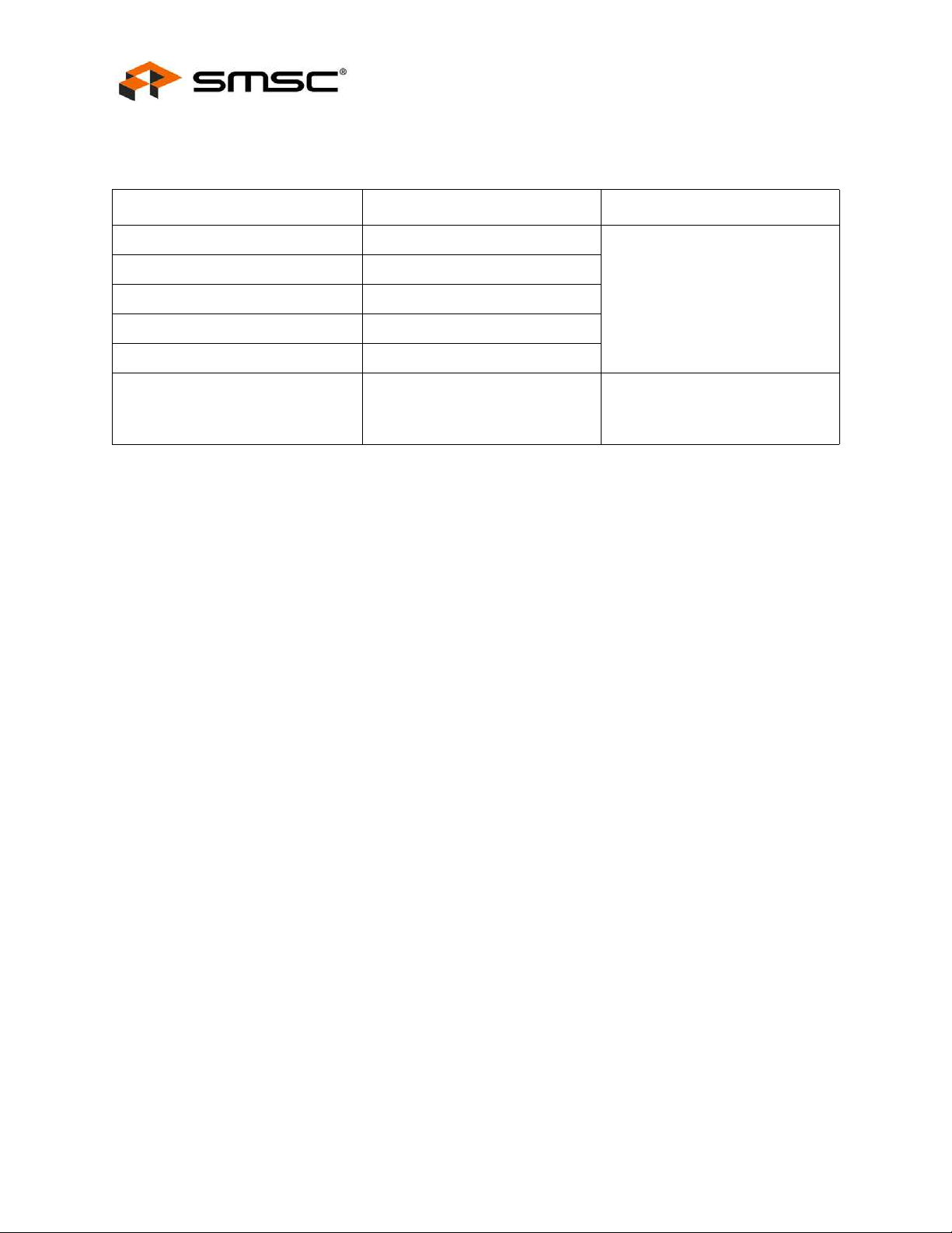
T able 3.1 ADDR_SEL Pin Decode
PULL-UP RESISTOR SMBUS ADDRESS ADDITIONAL FUNCTIONS
4.7k Ohm ±5% 0101_110(r/w)
6.8k Ohm ±5% 0101_111(r/w)
10k Ohm ±5% 0101_100(r/w)
15k Ohm ±5% 0101_101(r/w)
22k Ohm ±5% 1001_100(r/w)
None - CLK pin used as clock input
or output
33k Ohm ±5% 1001_101(r/w) CLK pin used to determine default
3.1.3 SMBus Data Bytes
All SMBus Data bytes are sent most significant bit first and composed of 8-bits of information.
3.1.4 SMBus ACK and NACK Bits
The SMBus client will acknowledge all data bytes that it receives (as well as the client add ress if it
matches and the ARA address if the ALERT# pin is asserted). This is done by the client device pulling
the SMBus Data line low after the 8th bit of each byte that is transmitted.
The Host will NACK (not acknowledge) the data received from the client by holding the SMBus data
line high after the 8th data bit has been sent.
3.1.5 SMBus Stop Bit
The SMBus Stop bit is defined as a transition of the SMBus Data line from a logic ‘0’ state to a logic
‘1’ state while the SMBus clock line is in a logic ‘1’ state. When the EMC2305 detects an SMBus Stop
bit has been communicating with the SMBus protocol, it will reset its client interface and prepare to
receive further communications.
3.1.6 SMBus Time-out
fan drive - see
CLK pin cannot be used as a clock
input or output
Section 4.5.1. The
The EMC2305 includes an SMBus timeout feature. Following a 30ms period of inactivity on the
SMBus, the device will time-out and reset the SMBus interface.
The SMBus timeout feature is disabled by default and can be en abled via clearing the DIS_TO bit in
the Configuration register (20h).
3.1.7 SMBus and I2C Compliance
The major difference between SMBus and I2C devices is highlighted here. For complete compliance
information refer to the SMBus 2.0 specification.
2
1. Minimum frequency for SMBus communications is 10kHz (I
2. The sla ve protocol will reset if the clock is held low for longer than 30ms (I2C has no timeout).
3. Th e slave protocol will reset if both the clock and data lines are held high for longer tha n 150us.
2
C devices do not support the Alert Response Address functionality (which is op tiona l for SMBus).
4. I
Revision 1.3 (05-18-11) 14 SMSC EMC2305
C has no minimum frequency).
DATASHEET
Page 15
Multiple RPM-Based PWM Fan Controller for Five Fans
Datasheet
5. Th e Block Read and Block Write protocols are only compliant with I2C data formatting. They do
not support SMBus formatting for Block Read and Block Write protocols.
3.2 SMBus Protocols
The EMC2305 is SMBus 2.0 compatible and supports Send Byte, Read Byte, Receive Byte and Write
Byte as valid protocols as shown below. It will respond to the Alert Response Address protocol but is
not in full compliance.
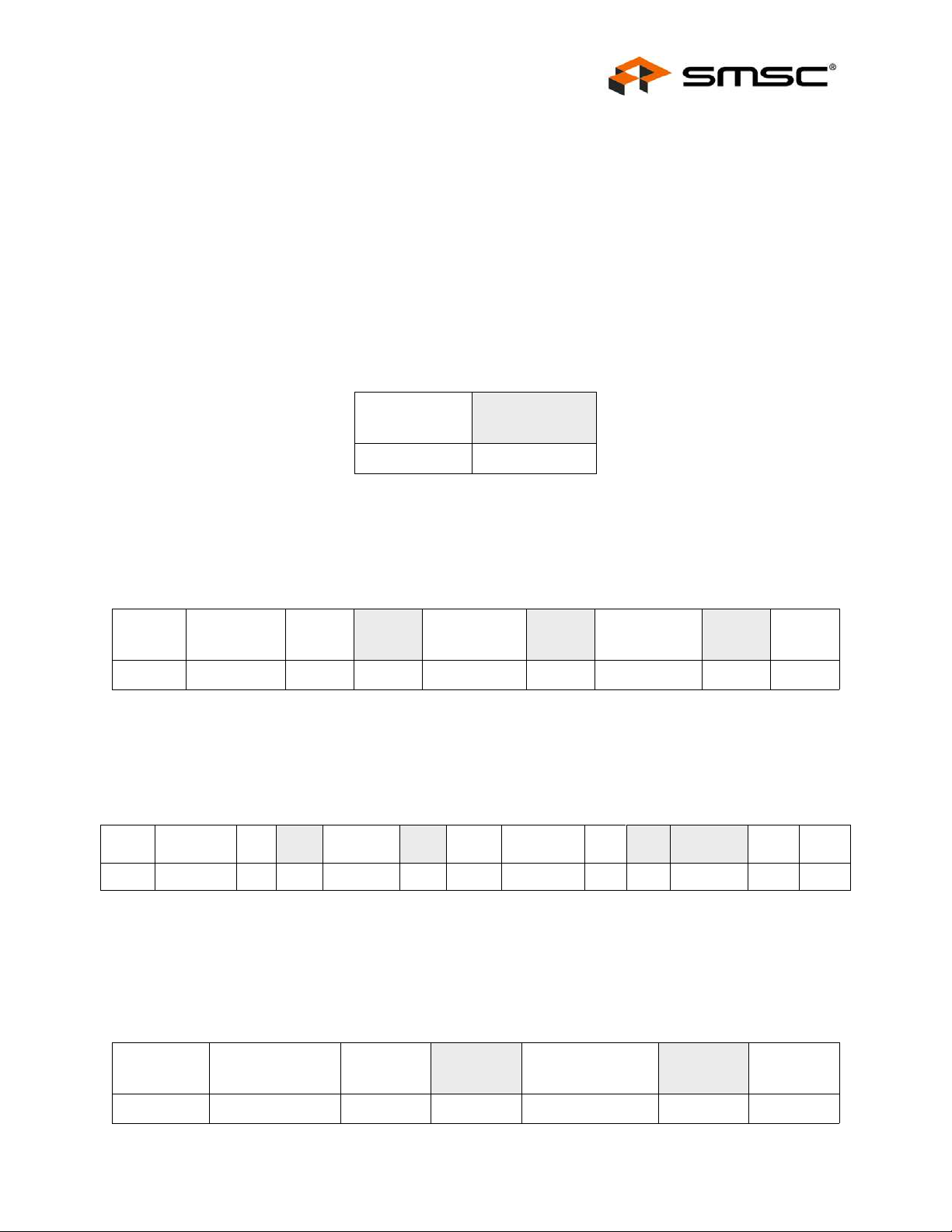
All of the below protocols use the convention in
Table 3.2. When reading the protocol blocks, th e value
of YYYY_YYYb should be replaced with the respective SMBus addresses.
Table 3.2 Protocol Format
DATA SENT
TO DEVICE
DATA SENT TO
THE HOST
# of bits sent # of bits sent
3.2.1 Write Byte
The Write Byte is used to write one byte of data to the registers as shown below Table 3.3.
Table 3.3 Write Byte Protocol
ST ART
SLAVE
ADDRESS WR
ACK
REGISTER
ADDRESS ACK
REGISTER
DATA ACK STOP
1 -> 0 YYYY_YYYb 0 0 XXh 0 XXh 0 0 -> 1
3.2.2 Read Byte
The Read Byte protocol is used to read one byte of data from the registers as show n in
Table 3.4.
Table 3.4 Read Byte Protocol
START SLAVE
1 -> 0 YYYY_YYYb 0 0 XXh 0 0 -> 1 YYYY_YYYb 1 0 XXh 1 0 -> 1
ADDRESS
ACK Register
WR
Address
ACK START Slave
Address
RD ACK Register
Data
NACK STOP
3.2.3 Send Byte
The Send Byte protocol is used to set the internal address register pointer to the correct address
location. No data is transferred during the Send Byte protocol as shown in
Table 3.5.
Table 3.5 Send Byte Protocol
START
SLA VE
ADDRESS WR ACK
REGISTER
ADDRESS ACK STOP
1 -> 0 YYYY_YYYb 0 0 XXh 0 0 -> 1
SMSC EMC2305 15 Revision 1.3 (05-18-11)
DATASHEET
Page 16
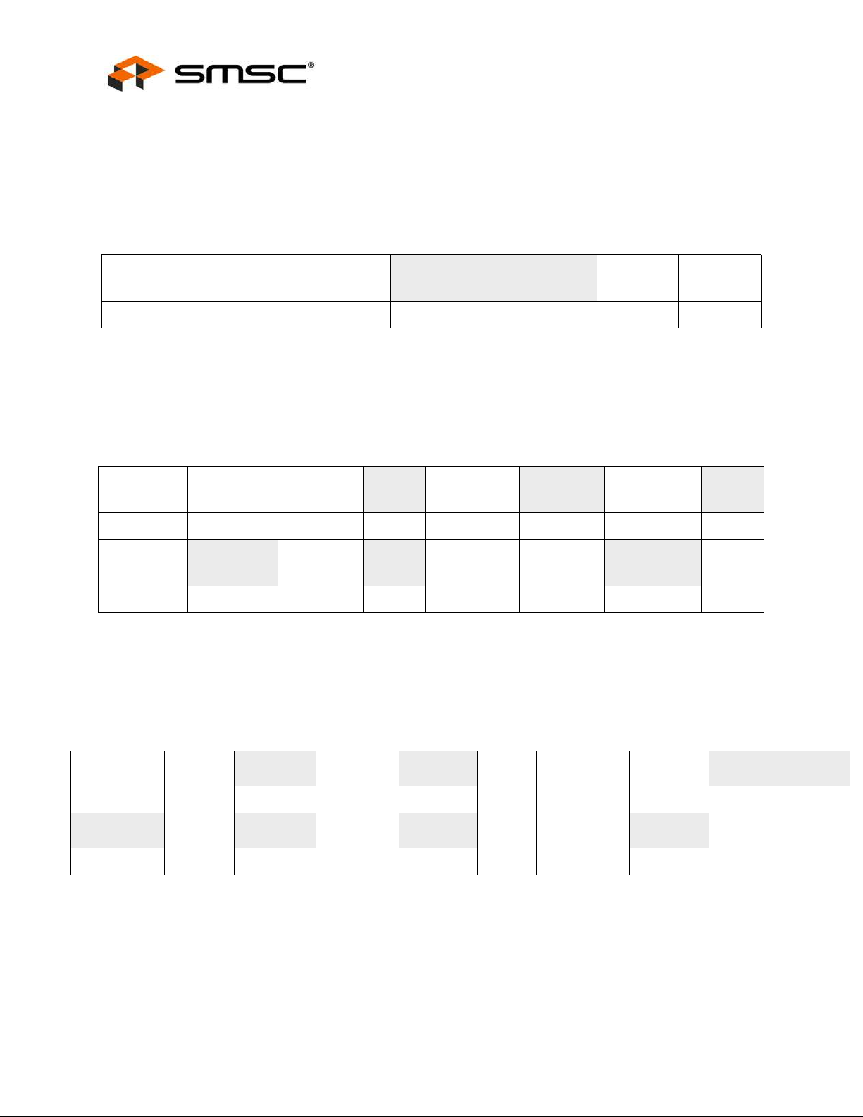
3.2.4 Receive Byte
The Receive Byte protocol is used to read data from a register when the internal register address
pointer is known to be at the right location (e.g. set via Send Byte). This is used for consecutive reads
of the same register as shown in
Multiple RPM-Based PWM Fan Controller for Five Fans
Datasheet
Table 3.6.
Table 3.6 Receive Byte Protocol
START
ADDRESS RD
ACK REGISTER DATA NACK STOP
1 -> 0 YYYY_YYYb 1 0 XXh 1 0 -> 1
3.2.5 Block Write Protocol
SLA VE
The Block Write is used to write multiple data bytes to a group of contiguous registers as shown in
Table 3.7. It is an extension of the Write Byte Protocol.
Table 3.7 Block Write Protocol
START
SLAVE
ADDRESS WR ACK
REGISTER
ADDRESS ACK
REGISTER
DATA ACK
1 ->0 YYYY_YYYb 0 0 XXh 0 XXh 0
REGISTER
DATA
ACK
REGISTER
DATA ACK . . .
REGISTER
DATA ACK STOP
XXh 0 XXh 0 . . . XXh 0 0 -> 1
3.2.6 Block Read Protocol
The Block Read is used to read multiple data bytes from a group of contiguous registers as sh own in
Table 3.8. It is an extension of the Read Byte Protocol.
Table 3.8 Block Read Protocol
START SLAVE
ADDRESS
WR
ACK REGISTER
ADDRESS
ACK START SLAVE
ADDRESS
RD ACK REGISTER
DATA
1->0 YYYY_YYYb 0 0 XXh 0 1 ->0 YYYY_YYYb 1 0 XXh
ACK
REGISTER
DATA
ACK REGISTER
DATA
ACK REGISTER
DATA
ACK . . . REGISTER
DATA
NACK STOP
0 XXh 0 XXh 0 XXh 0 . . . XXh 1 0 -> 1
3.2.7 Alert Response Address
The ALERT# output can be used as a processor interrupt or as an SMBus Alert when configured to
operate as an interrupt.
When it detects that the ALERT# pin is asserted, the host will send the Alert Response Address (ARA)
to the general address of 0001_100xb. All devices with active i nterrupts will respond with their client
address as shown in
Revision 1.3 (05-18-11) 16 SMSC EMC2305
Table 3.9.
DATASHEET
Page 17

Multiple RPM-Based PWM Fan Controller for Five Fans
Datasheet
Table 3.9 Alert Response Address Protocol
ALERT
START
RESPONSE
ADDRESS RD
ACK
DEVICE
ADDRESS NACK STOP
1 -> 0 0001_100b 1 0 YYYY_YYYb 1 0 -> 1
The EMC2305 will respond to the ARA in the following way if the ALERT# pin is asserted.
1. Send Slave Address and verify that full slav e address was sent (i.e. the SMBus communication
from the device was not prematurely stopped due to a bus contention event).
2. Set the MASK bit to clear the ALERT# pin.
SMSC EMC2305 17 Revision 1.3 (05-18-11)
DATASHEET
Page 18
Chapter 4 Product Description
EMC 2305
SMCLK
SMDATA
ALERT#
VDD
3.3V
MCU
ADDR_SEL
GND
32.768KHz Clock
Input or O utput
CLK
TACH3
tachometer
PWM3
Drive
Circuit
TACH4
tachometer
PWM4
Drive
Circuit
TACH5
tachometer
PWM5
Drive
Circuit
TACH1
tachometer
PWM1
Drive
Circuit
TACH2
tachometer
PWM2
Drive
Circuit
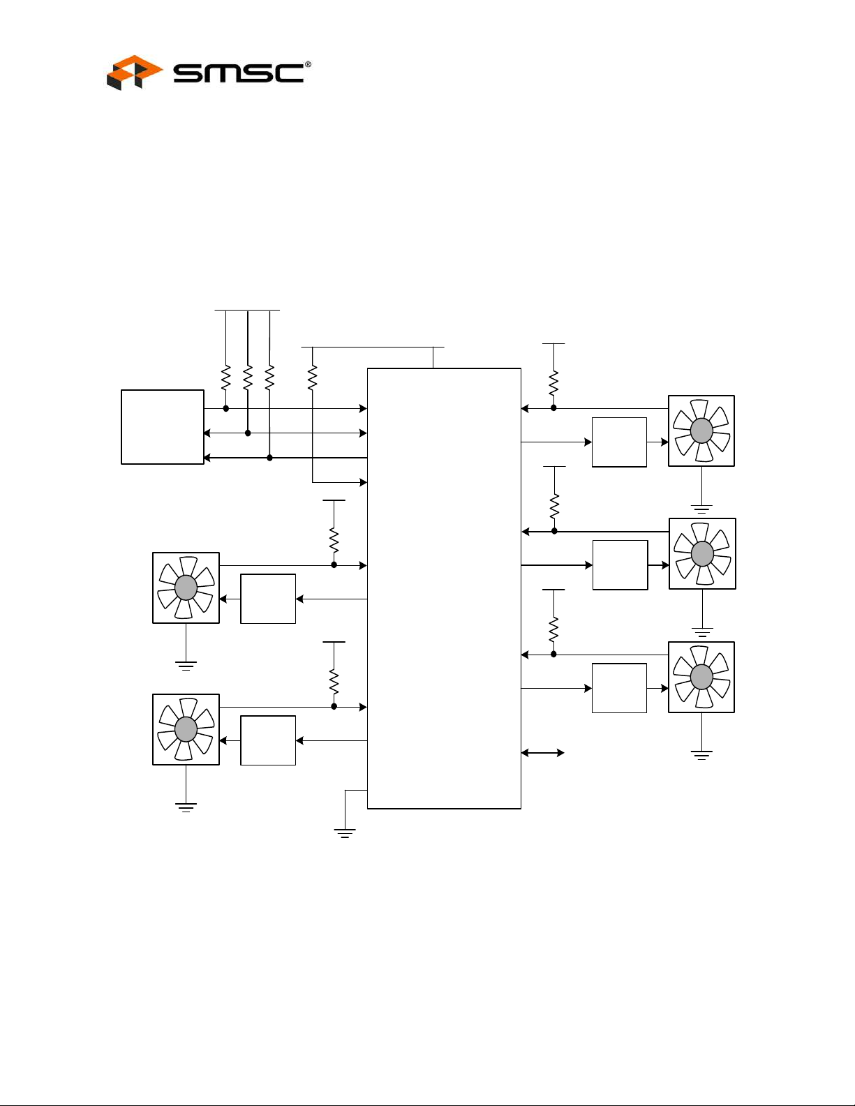
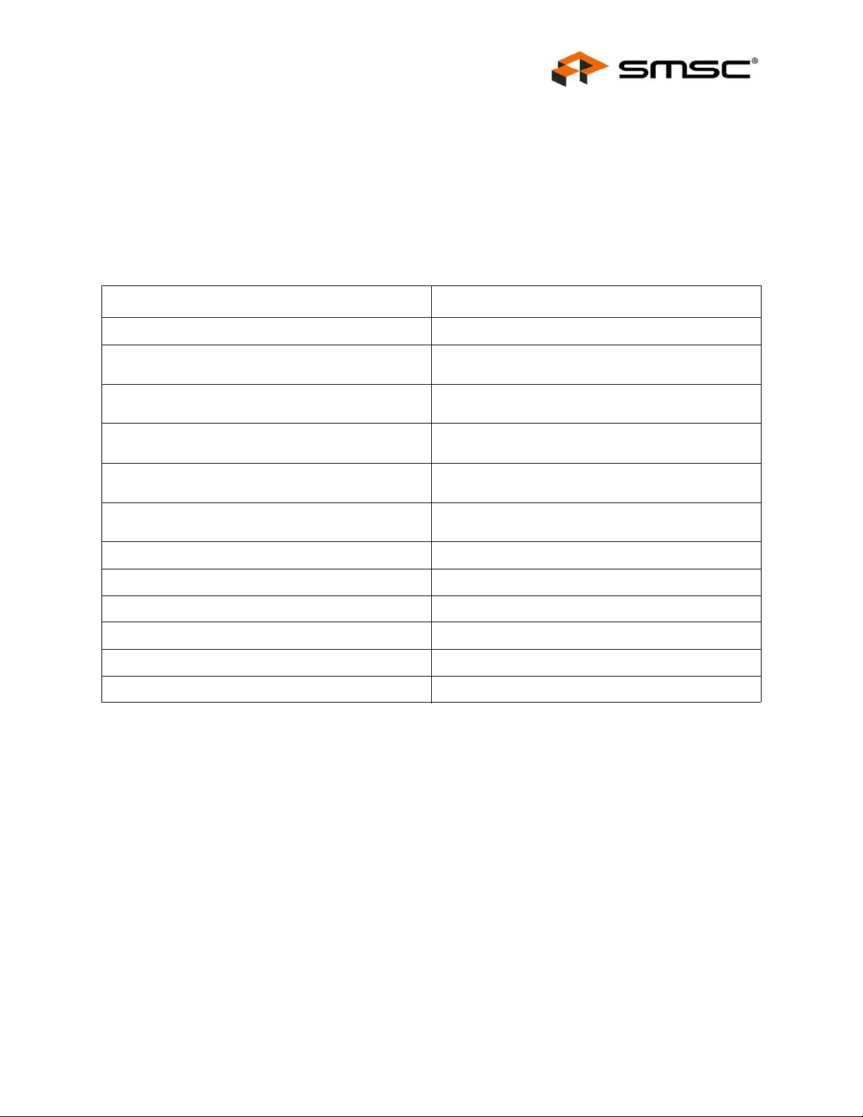
The EMC2305 is an SMBus compliant fan controller with five programmable frequency PWM fan
drivers. The fan drivers can be operated using two modes: the RPM-based Fan Speed Control
Algorithm or the direct fan drive setting.
Figure 4.1 shows a system diagram of the EMC2305.
Multiple RPM-Based PWM Fan Controller for Five Fans
Datasheet
4.1 Fan Control Modes of Operation
The EMC2305 has two modes of operation for each fan driver. Each mode of operation uses the Ramp
Revision 1.3 (05-18-11) 18 SMSC EMC2305
Rate control and Spin Up Routine.
1. Direct Setting Mode - in this mode of operation, the user directly controls the fan drive setting.
Updating the Fan Driver Setting Register (see
Ramp Rate control is optional and enabled via the EN_RRC b its.
Figure 4.1 System Diagram of EMC2305
DATASHEET
Section 5.7) will instantly update the PWM fan drive.
Page 19
Multiple RPM-Based PWM Fan Controller for Five Fans
Datasheet
Whenever the Direct Setting Mode is enabled, the current drive will be changed to what was
last written into the Fan Driver Setting Register.
2. Fan Speed Control Mode (FSC) - in this mode of operation, the user determines a target
tachometer count and the PWM drive setting is automatically updated to achieve this target speed.
The algorithm uses the Spin Up Routine and has user definable ramp rate controls.
This mode is enabled setting the EN_ALGO bit in the Fan Configuration Register.
Table 4.1 Fan Controls Active for Operating Mode
DIRECT SETTING MODE FSC MODE
Fan Driver Setting (read / write) Fan Driver Setting (read only)
EDGES[1:0] EDGES[1:0]
- RANGE[1:0]
UPDATE[2:0]
(Fan Configuration)
LEVEL
(Spin Up Configuration)
SPINUP_TIME[1:0]
(Spin Up Configuration)
Fan Step Fan Step
- Fan Minimum Drive
Valid TACH Count Valid TACH Count
- TACH Target (read / write)
TACH Reading TACH Reading
- DRIVE_FAIL_CNT[1:0] and Drive Band Fail Registers
(Fan Configuration)
(Fan Configuration)
UPDATE[2:0]
(Fan Configuration)
LEVEL
(Spin Up Configuration)
SPINUP_TIME[1:0]
(Spin Up Configuration)
4.2 PWM Fan Driver
The EMC2305 supports 5 PWM output drivers. Each output driver can be configu red to operate as an
open-drain (default) or push-pull driver and each driver can be configured with normal or inverse
polarity. Additionally, the PWM frequencies are independently programmable with ranges from 9.5Hz
to 26kHz in four programmable frequency bands.
4.3 RPM-based Fan Speed Control Algorithm (FSC)
The EMC2305 includes 5 RPM-based Fan Speed Control Algorithms. Each algorithm operates
independently and controls a separate fan driver. Each algorithm is controlled manually (by setting the
target fan speed).
This fan control algorithm uses Proportional, In tegral, and Derivative terms to automatically approach
and maintain the system’s desired fan speed to an accuracy directly proportional to the accuracy of
the clock source.
The desired tachometer count is set by the user inputting the desired number of 32.768kHz cycles that
occur per fan revolution. This is done by manually setting the TACH Target Register. The user may
SMSC EMC2305 19 Revision 1.3 (05-18-11)
DATASHEET
Page 20

Multiple RPM-Based PWM Fan Controller for Five Fans
change the target count at any time. The user may also set the target count to FF h in order to disable
the fan driver for lower current operation.
For example, if a desired RPM rate for a 2-pole fan is 3000 RPMs, then the user would input the
hexidecimal equivalent of 1296 (51h in the TACH Target Register). This number represents the number
of 32.768KHz cycles that would occur during the time it takes the fan to complete a single revolution
when it is spinning at 3000RPMs.
The EMC2305’s RPM-based Fan Speed Control Algorithm has programmable configuration settings
for parameters such as ramp-rate control and spin up conditions. The fan driver automatically detects
and attempts to alleviate a stalled/stuck fan condition while also asserting the ALERT# pin. The
EMC2305 works with fans that operate up to 16,000 RPMs and provi de a valid tachometer signal.
The fan controller will function either wi th an externally supplied 32.768kHz clock source or with it’s
own internal 32kHz oscillator depending on the required accuracy. The EMC2305 offers a clock output
that enables additional devices to be slaved to the same clock source.
4.3.1 Programming the RPM-based Fan Speed Control Algorithm
The RPM-based Fan Speed Control Algorithm is disabled upon device power up. The following
registers control the algorithm. The EMC2305 fan control regi sters are pre-loaded with defaults that
will work for a wide variety of fans so only the TACH Target Register is required to set a fan speed.
The other fan control registers can be used to fine-tune the algorithm behavior based on application
requirements.
Datasheet
Note that steps 1 - 6 are optional and need only be performed if the default settings do not provide
the desired fan response.
1. Set the Spin Up Configuration Register to the Spin Up Level and Spin Time desired.
2. Set the F an Step Register to the desired step size.
3. Set th e Fan Minimum Drive Register to the minimum drive value that will maintain fan operation.
4. Set th e Update Time and Edges options in the Fan Configuration Register.
5. Set the Valid TACH Count Register to the highest tach count that indicates the fan is spinning.
Refer to
ranges (500, 1k, 2k, 4k).
6. Set the TACH Target Register to the desired tachometer count.
7. Enab le the RPM-based Fan Speed Control Algorithm by setting the EN_ALGO bit.
AN17.4 RPM to TACH Counts Conversion for examples and tables for supported RPM
4.4 Tachometer Measurement
The tachometer measurement circuitry is used in conjunction with the RPM-based Fan Speed Control
Algorithm to update the fan driver output. Additionally, it can be used in Direct Setting mode as a
diagnostic for host based fan control.
This method monitors the TACHx signal in real time. It constantly updates the tachometer
measurement by reporting the number of clocks between a user prog rammed number of edges on the
TACHx signal (see
The tachometer measurement provides fast response times for the RPM-based Fan Speed Control
Algorithm and the data is presented as a count value that represents the fan RPM period.
Table 5.12).
APPLICATION NOTE: The tachometer measurement method works independently of the drive settings. If the
device is put into Direct Setting and the fan drive is set at a level that i s lower than the fan
can operate (including zero drive), then the tachometer measurement may signal a Stalled
Fan condition and assert an interrupt.
Revision 1.3 (05-18-11) 20 SMSC EMC2305
DATASHEET
Page 21
Multiple RPM-Based PWM Fan Controller for Five Fans
Datasheet
4.4.1 Stalled Fan
A Stalled fan is detected if the tach counter exceeds the user-programmable Valid TACH Count setting.
If a stall is detected, the device will flag the fan as stalled and trigger an interrupt.
If the RPM-based Fan Speed Control Algorithm is enabled, the algorithm will automatically attempt to
restart the fan until it detects a valid tachometer level or is disabled.
The FAN_STALL Status bit indicates that a stalled fan was detected. This bit is checked conditionally
depending on the mode of operation.
Whenever the Direct Setting Mode or the Spin Up Routine is enabled, the FAN_STALL interrupt
will be masked for the duration of the programme d Spin Up Time (see
to reach a valid speed without generating unnecessary interrupts.
In Direct Setting Mode, whenever the TACH Reading Register value exceeds the Valid TACH Count
Register setting, the FAN_STALL status bit will be set.
When using the RPM-based Fan Speed Control Algorithm, the stalled fan condition is checked
whenever the Update Time is met and the fan drive setting is updated. It is not a continuous check.
4.4.2 Aging Fan or Invalid Drive Detection
This is useful to detect aging fan conditions (where the fan’s natural maximum speed degrades over
time) or a speed setting that is faster than the fan is capable of. The EMC230 5 contains circuitry that
detects that the programmed fan speed can be reached by the fan. If the target fan speed cannot be
reached within a user defined band of tach counts at maximum drive, the DRIVE_FAIL status bits are
set and the ALERT# pin is asserted.
Table 5.22) to allow the fan
4.5 CLK Pin
The CLK pin has multiple functionality as determined by the pul l-up decode of the ADDR_SEL pin and
the settings of the Configuration register. The functionality associated with the CLK pin upon device
power up is independent of the CLK pin functionality after the device has been configure d.
4.5.1 Pull Up Decode
If additional functionality is enabled via the ADDR_SEL pin (see
should be configured with a pull-up resistor to VDD and should not be us ed. The value of the pull-up
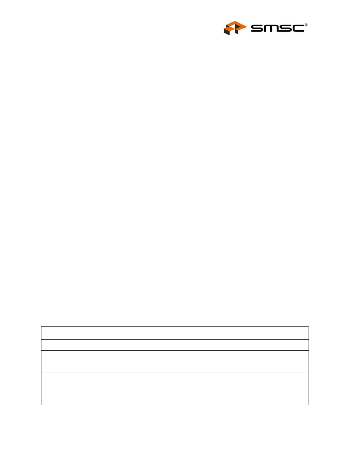
resistor on the CLK pin is used to determine the default drive state of all fan drivers as shown in
Table 4.2.
PULL-UP RESISTOR FAN DEFAULT DRIVE SETTING
4.7k Ohm ±5% 0% - OFF
6.8k Ohm ±5% 30%
10k Ohm ±5% 50%
15k Ohm ±5% 75%
22k Ohm ±5% 100%
Section 3.1.2), then the CLK pin
T a ble 4.2 CLK Pin Pull-Up Decode
33k Ohm ±5% 0% - OFF
SMSC EMC2305 21 Revision 1.3 (05-18-11)
DATASHEET
Page 22

4.5.2 External Clock
The EMC2305 allows the user to choose between supplying an external 32.768kHz clock or use of
the internal 32kHz oscillator to measure the tachometer si gnal. This clock source is used by the RPMbased Fan Speed Control Algorithm to calculate the current fan speed. This fan controller accuracy is
directly proportional to the accuracy of the clock source.
When this function is used, the external clock is driven into the de vice via the CLK pin.
4.5.3 Internal Clock
Alternately, the EMC2305 may be configured to use its internal clock as a clock output to drive other
fan driver devices. When configured to operate in this mode, the device uses its internal clock for
tachometer reading and drives the CLK pin using a push-pull driver.
4.6 Spin Up Routine
The EMC2305 also contains programmable circuitry to control the spin up behavior of the fan driver
to ensure proper fan operation.
The Spin Up Routine is initiated in Direct Setting mode when the setting value changes from 00h to
anything else.
Multiple RPM-Based PWM Fan Controller for Five Fans
Datasheet
When the Fan Speed Control Algorithm is enabled, the Spin Up Routine is initiated under the following
conditions:
1. The TACH Target Register value changes from a value of FFh to a value that is less than the Valid
TACH Count (see
2. Th e RPM-based Fan Speed Control Algorithm’s measured TACH Reading Register value is greater
than the Valid TACH Count setting.
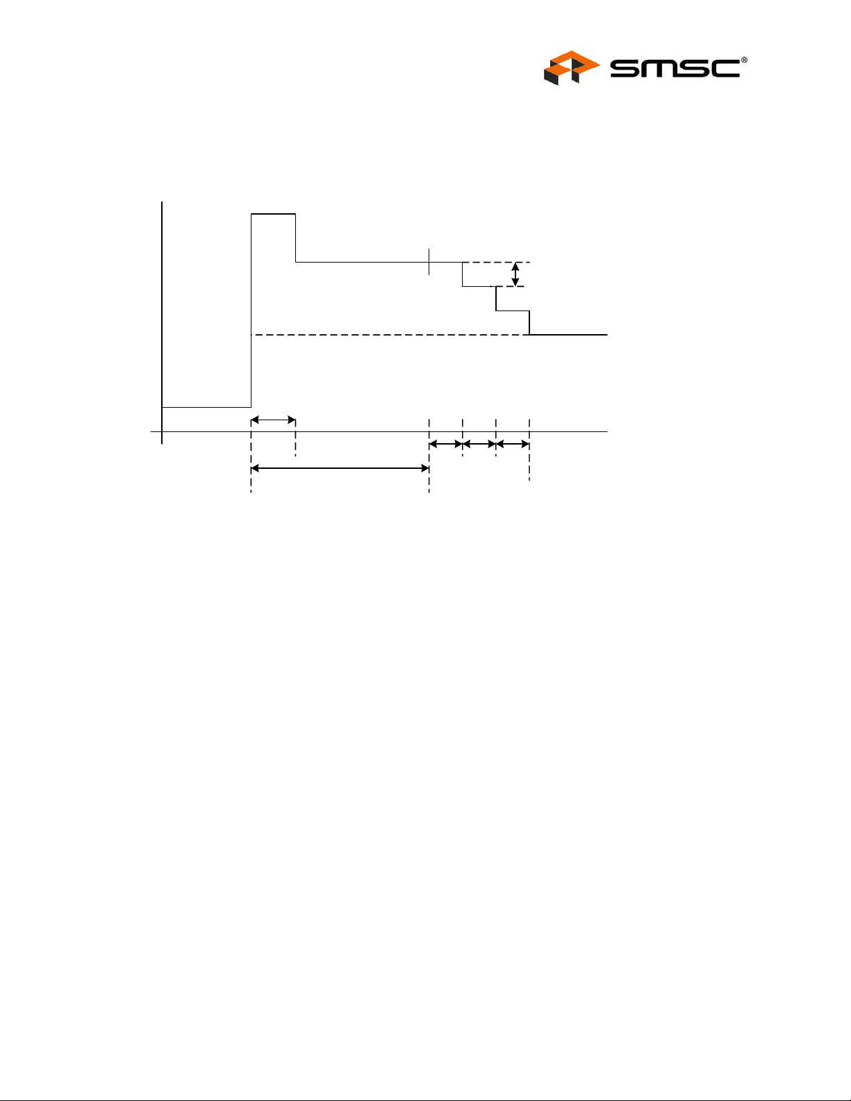
When the Spin Up Routine is operating, the fan driver is set to full scale (optional) for one quarter of
the total user defined spin up time. For the remaining spin u p time, the fan driver output is set at a
user defined level (30% through 65% drive).
After the Spin Up Routine has finished, the EMC2305 measures the TACHx signal. If the measured
TACH Reading Register value is higher than the Valid TACH Count Register setting, the FAN_SPIN
status bit is set and the Spin Up Routine will automatically attempt to restart the fan.
Figure 4.2 shows an example of the Spin Up Routine in response to a programmed fan speed change
based on the first condition above.
Section 5.15).
Revision 1.3 (05-18-11) 22 SMSC EMC2305
DATASHEET
Page 23
Multiple RPM-Based PWM Fan Controller for Five Fans
100%
(optional)
30% through 65%
Algorithm controlled drive
Fan Step
Spin Up Time
¼ of Spin U p T im e
Update Time
Target Count
Changed
Target Count
Reached
New Target Count
Prev Target
Count = FFh
Check TACH
Datasheet
4.6.1 Power Up Options
The EMC2305 allows for one of four fan speed options upon device power up dependin g on the status
of the pull-up resistor on the ADDR_SEL pin and the CLK pin. If the ADDR_SEL pin decode enables
the CLK pin (see
the default fan drive setting (see
If the Fan drive setting is set at a non-zero value (as de termined by the CLK pin), then the drive setting
will be set to the desired setting. The Spin Up Routine will not be activated. This function does not
disable the Watchdog timer which will continue to function normally. See
4.7 Ramp Rate Control
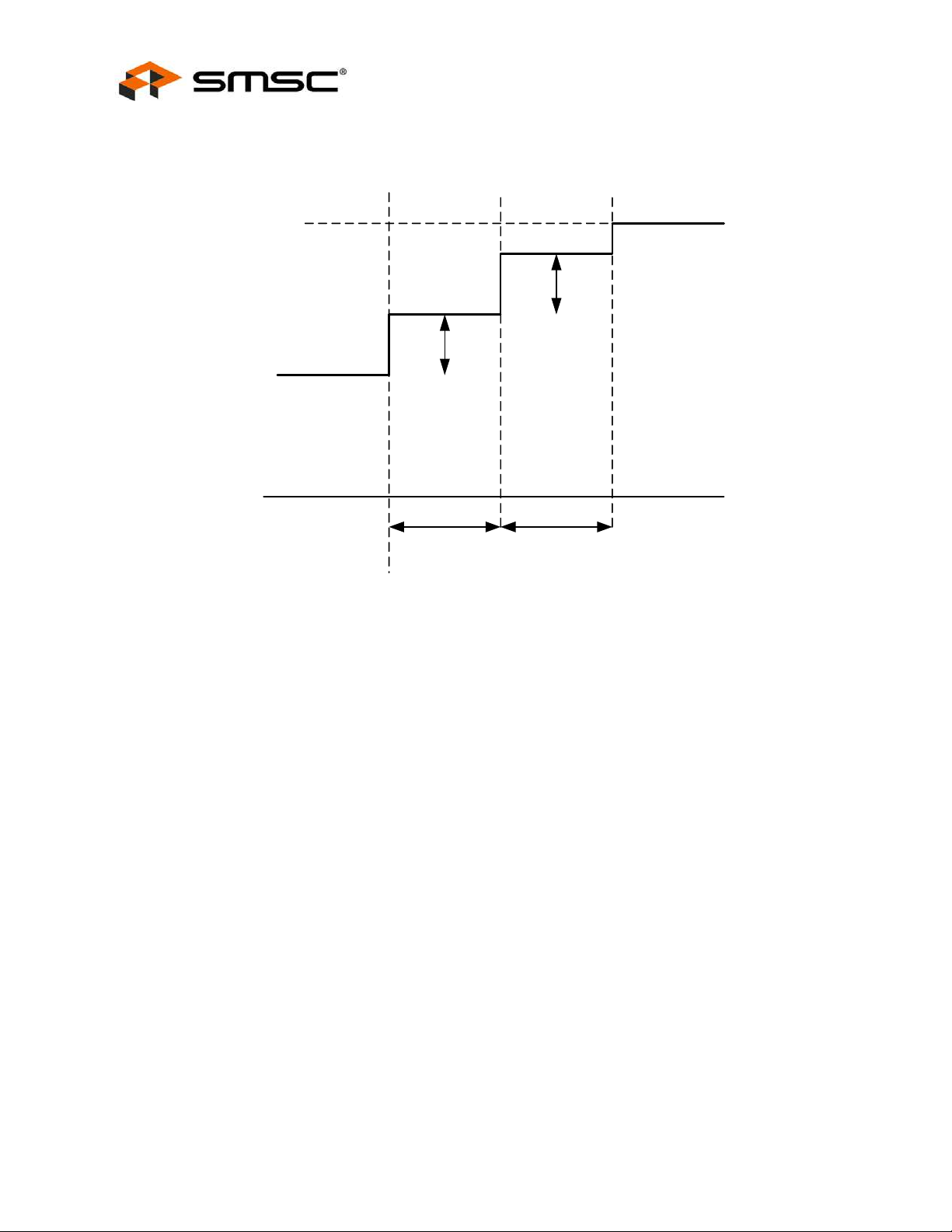
The Fan Driver can be configured with automatic ramp rate control. Ramp rate control is accomplish ed
by adjusting the drive output settings based on the Maximum Fan Step Register settings and the
Update Time settings.
If the RPM-based Fan Speed Control Algorithm is used, then this ramp rate control is automatically
used. The user programs a maximum step size for the fan drive setting and an update time. The
update time varies from 100ms to 1.6s while the fan drive maximum step can vary from 1 count to 31
counts.
When a new fan drive setting is entered, the delta from the next fan drive setting and th e previous fan
drive setting is determined. If this delta is greater than the Max Step settings, then the fan drive setting
is incrementally adjusted every 100ms to 1.6s as determi ned by the Update Time until the target fan
drive setting is reached. See
Table 3.1), then the value of the pul l-up resistor on the CLK pin is used to determi ne
Figure 4.2 Spin Up Routine
Section 4.5.1).
Section 4.8.
Figure 4.3.
SMSC EMC2305 23 Revision 1.3 (05-18-11)
DATASHEET
Page 24
Multiple RPM-Based PWM Fan Controller for Five Fans
Previous
Settin g
Next Desired
Setting
Max
Step
Max
Step
Update
Time
Update
Time
Setting Changed
Datasheet
Figure 4.3 Ramp Rate Control
4.8 Watchdog Timer
The EMC2305 contains an internal Watchdog Timer for all fan drivers. The Watchdog timer monitors
the SMBus traffic for signs of activity and works in two different modes based upon device operation.
These modes are Power Up Operation and Continuous Operation as describe d below.
For either mode of operation, if four (4) seconds elapse without activity detected by the host, then the
watchdog will be triggered and the following will oc cur:
1. The WATCH status bit will be set.
2. Th e fan driver will be set to full scale drive. It will remain at full scale drive un til it is disabled.
3. Th e ALERT# pin is asserted.
APPLICATION NOTE: When the Watchdog timer is activated, the Fan Speed Control Algorithm is automatically
disabled. Disabling the Watchdog will not automatically set the fan drive nor re-activate the
Fan Speed Control Algorithm. This must be done manually.
4.8.1 Power Up Operation
The Watchdog Timer only starts immediately after power-up. Once it has been triggered or deactivated,
it will not restart although it can be configured to operate i n Continuous opera tion. While the Watchdog
timer is active, the device will not check for a Stalled Fan condition.
Revision 1.3 (05-18-11) 24 SMSC EMC2305
DATASHEET
Page 25

Multiple RPM-Based PWM Fan Controller for Five Fans
Datasheet
In the Power Up Operation, the Watchdog Timer is disabled by any of the following actions:
1. Writing the Fan Setting Register will disable the Watchdog Timer.
2. Enab ling the RPM-based Fa n Speed Control Algorithm by setting the EN_ALGO bit will disable the
Watchdog Timer. The fan driver will be set based on the RPM-based Fan Speed Control Algorithm.
Writing any other configuration registers will not disable the Watchdog Timer upon power up.
4.8.2 Continuous Operation
When configured to operate in Continuous Operation, the Watchdog timer will start immediately. The
timer will be reset by any access (read or write) to the SMBus register set. The four second Watchdog
timer will restart upon completion of SMBus activity.
SMSC EMC2305 25 Revision 1.3 (05-18-11)
DATASHEET
Page 26
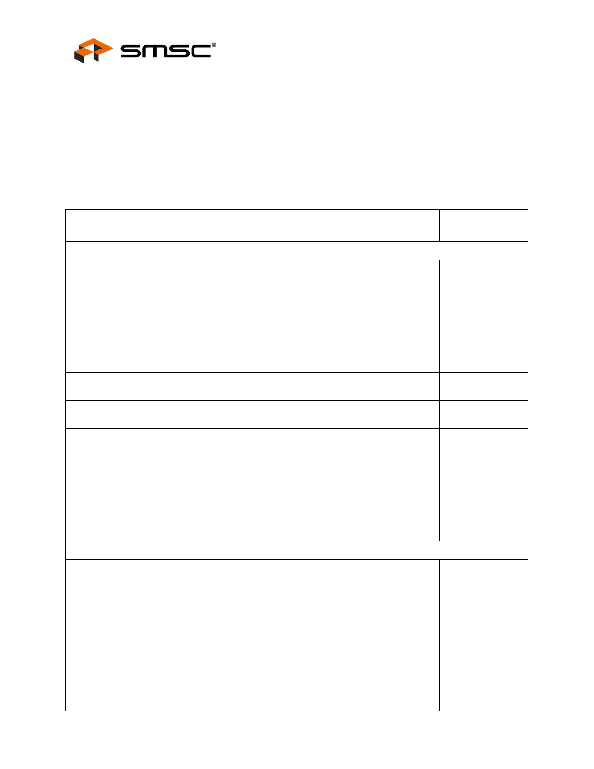
Chapter 5 Register Set
5.1 Register Map
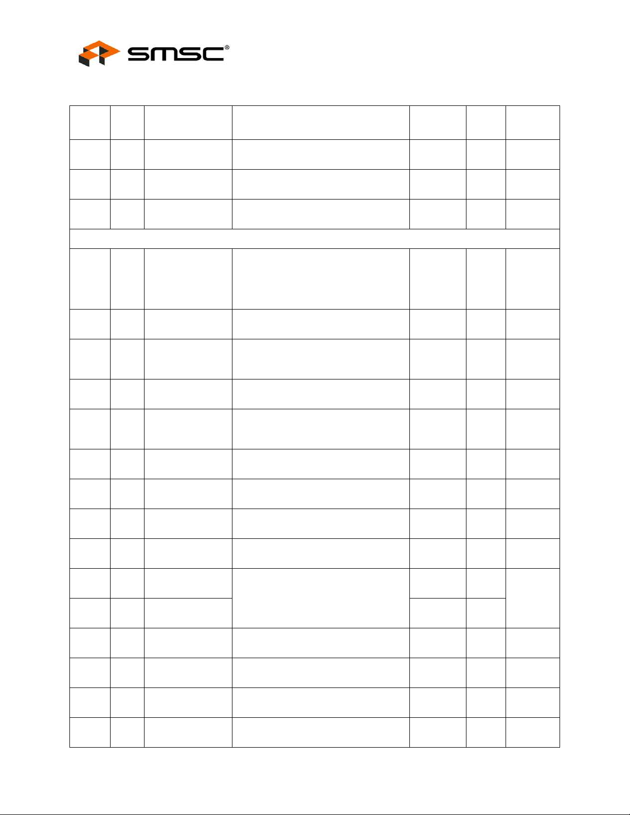
The following registers are accessible through the SMBus Interface. All register bits marked as ‘-’ will
always read ‘0’. A write to these bits will have no effect.
Table 5.1 EMC2305 Register Set
Multiple RPM-Based PWM Fan Controller for Five Fans
Datasheet
REGISTER
ADDR R/W
20h R/W Configuration
24h R-C Fan Status
25h R-C Fan Stall Status
26h R-C F an Spin Status
27h R-C Drive Fail Status
29h R/W
2Ah R/W
2Bh R/W
2Ch R/W
NAME FUNCTION
Fan Interrupt
Enable Register
PWM Polarity
Config
PWM Output
Config
PWM Base
Frequency 1
DEFAULT
VALUE LOCK PAGE
Configuration and control
Configures the clocking and watchdog
functionality
Stores the status bits for the RPM-
based Fan Speed Control Algorithm
Stores status bits associated with a
stalled fan
Stores status bits associated with a
spin-up failure
Stores status bits associated with drive
failure
Controls the masking of interrupts on all
fan related channels
Configures Polarity of all PWM drivers 00h No
Configures Output type of PWM drivers 00h No
Selects the base frequency for PWM
outputs 5 - 4
40h SW L
00h No
00h No
00h No
00h No
00h No
00h No
Page 31
Page 32
Page 32
Page 32
Page 32
Page 33
Page 34
Page 34
Page 35
2Dh R/W
30h R/W Fan 1 Setting
31h R/W PWM 1 Divi de
32h R/W
33h R/W
Revision 1.3 (05-18-11) 26 SMSC EMC2305
PWM Base
Frequency 2
Fan 1
Configuration 1
Fan 1
Configuration 2
Selects the base frequency for PWM
outputs 3 - 1
Fan 1 Control Registers
Always displays the most recent fan
driver input setting for Fan 1. If the
RPM-based Fan Speed Control
Algorithm is disabled, allows direct user
control of the fan driver.
Stores the divide ratio to set the
frequency for Fan 1
Sets configuration values for the RPM-
based Fan Speed Control Algorithm for
the Fan 1 driver
Sets additional configuration values for
the Fan 1 driver
00h No
00h No
01h No
2Bh No
28h SW L
Page 35
Page 36
Page 36
Page 37
Page 38
DATASHEET
Page 27
Multiple RPM-Based PWM Fan Controller for Five Fans
Datasheet
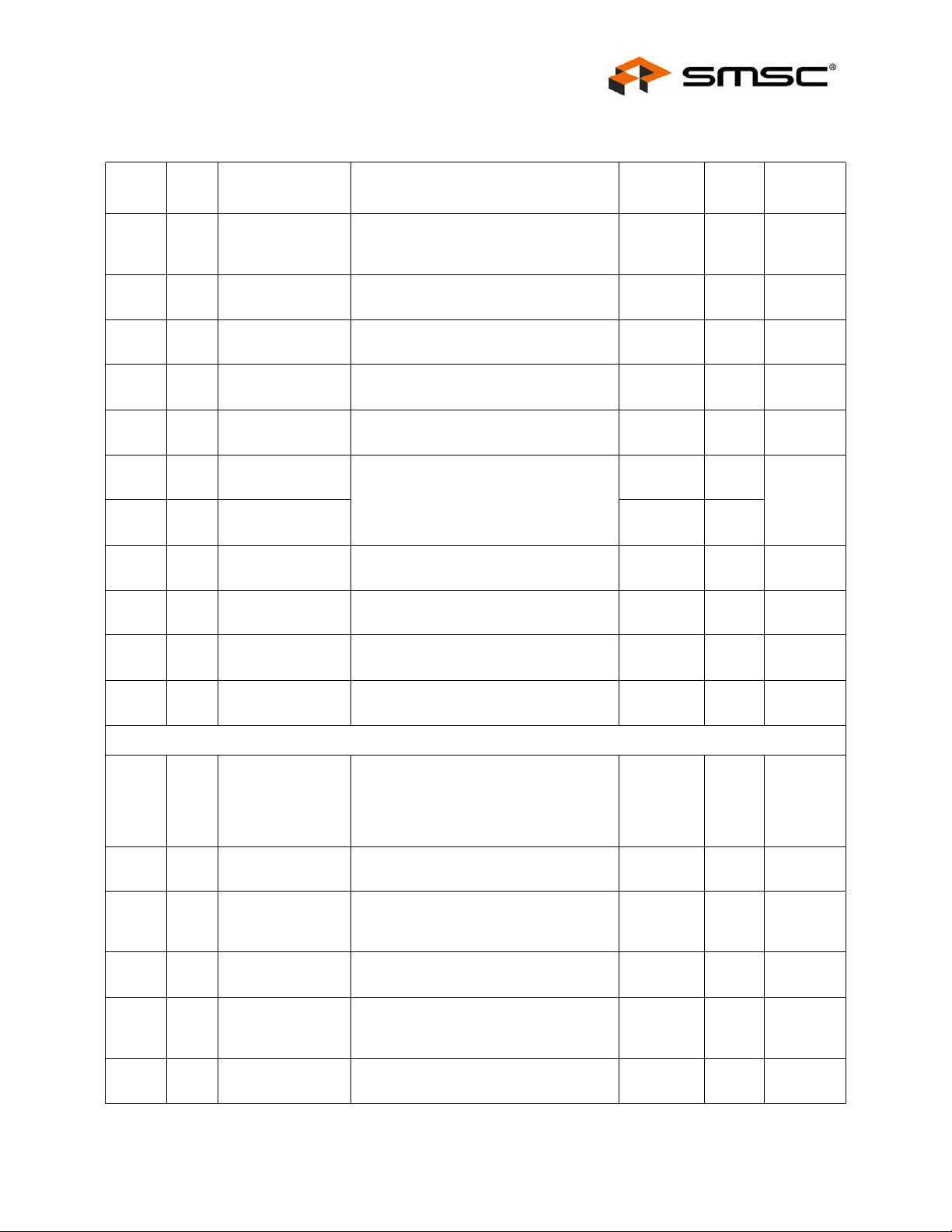
Table 5.1 EMC2305 Register Set (continued)
ADDR R/W
NAME FUNCTION
35h R/W Gain 1
REGISTER
36h R/W
Fan 1 Spin Up
Configuration
37h R/W Fan 1 Max Step
38h R/W
39h R/W
3Ah R/W
3Bh R/W
3Ch R/W
3Dh R/W
Fan 1 Minimum
Drive
Fan 1 Valid TACH
Count
Fan 1 Drive Fail
Band Low Byte
Fan 1 Drive Fail
Band High Byte
TACH 1 Target
Low Byte
TACH 1 Target
High Byte
Holds the gain terms used by the RPMbased Fan Speed Control Algorithm for
the Fan 1 driver
Sets the configuration values for Spin
Up Routine of the Fan 1 driver
Sets the maximum change per update
for the Fan 1 driver
Sets the minimum drive value for the
Fan 1 driver
Holds the tachometer reading that
indicates Fan 1 is spinning properly
Stores the number of Tach counts used
to determine how the actual fan speed
must match the target fan speed at full
scale drive
Holds the target tachometer reading low
byte for Fan 1
Holds the target tachometer reading
high byte for Fan 1
DEFAULT
VALUE LOCK PAGE
2Ah SWL Page 40
19h SW L
10h SW L
66h
(40%)
SWL
F5h SWL
Page 41
Page 43
Page 44
Page 44
00h SW L
Page 45
00h SW L
F8h No
FFh No
Page 46
Page 46
3Eh R
3Fh R
TACH 1 Reading
High Byte
TACH 1 Reading
Low Byte
40h R/W Fan 2 Setting
41h R/W PWM 2 Divi de
42h R/W
43h R/W
Fan 2
Configuration1
Fan 2
Configuration 2
45h R/W Gain 2
46h R/W
Fan 2 Spin Up
Configuration
Holds the tachometer reading high byte
for Fan 1
Holds the tachometer reading low byte
for Fan 1
Fan 2 Control Registers
Always displays the most recent fan
driver input setting for Fan 2. If the
RPM-based Fan Speed Control
Algorithm is disabled, allows direct user
control of the fan driver.
Stores the divide ratio to set the
frequency for Fan 2
Sets configuration values for the RPM-
based Fan Speed Control Algorithm for
Fan 2
Sets additional configuration values for
the Fan 2 driver
Holds the gain terms used by the RPMbased Fan Speed Control Algorithm for
Fan 2
Sets the configuration values for Spin
Up Routine of the Fan 2 driver
FFh No
F8h No
00h No
01h No
2Bh No
28h SW L
2Ah SWL
19h SW L
Page 47
Page 47
Page 36
Page 36
Page 37
Page 38
Page 40
Page 41
SMSC EMC2305 27 Revision 1.3 (05-18-11)
DATASHEET
Page 28
Multiple RPM-Based PWM Fan Controller for Five Fans
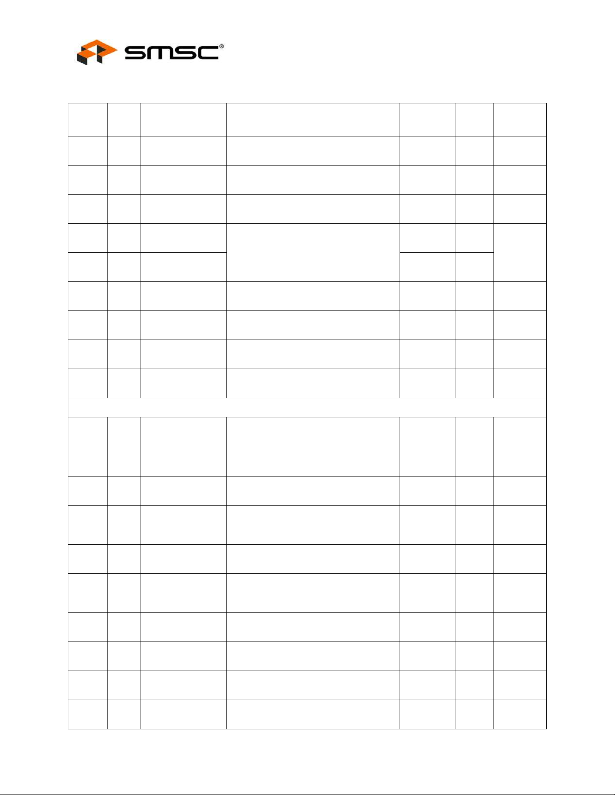
Table 5.1 EMC2305 Register Set (continued)
Datasheet
ADDR R/W
NAME FUNCTION
47h R/W Fan 2 Max Step
REGISTER
48h R/W
49h R/W
4Ah R/W
4Bh R/W
4Ch R/W
4Dh R/W
4Eh R
4Fh R
Fan 2 Minimum
Drive
Fan 2 Valid TACH
Count
Fan 2 Drive Fail
Band Low Byte
Fan 2 Drive Fail
Band High Byte
TACH 2 Target
Low Byte
TACH 2 Target
High Byte
TACH 2 Reading
High Byte
TACH 2 Reading
Low Byte
Sets the maximum change per update
for Fan 2
Sets the minimum drive value for the
Fan 2 driver
Holds the tachometer reading that
indicates Fan 2 is spinning properly
Stores the number of Tach counts used
to determine how the actual fan speed
must match the target fan speed at full
scale drive
Holds the target tachometer setting low
byte for Fan 2
Holds the target tachometer setting high
byte for Fan 2
Holds the tachometer reading high byte
for Fan 2
Holds the tachometer reading low byte
for Fan 2
DEFAULT
VALUE LOCK PAGE
10h SW L
66h
(40%)
SWL
F5h SWL
Page 43
Page 44
Page 44
00h SW L
Page 45
00h SW L
F8h No
FFh No
FFh No
F8h No
Page 46
Page 46
Page 47
Page 47
50h R/W Fan 3 Setting
51h R/W PWM 3 Divi de
52h R/W
53h R/W
Fan 3
Configuration 1
Fan 3
Configuration 2
55h R/W Gain 3
56h R/W
Fan 3 Spin Up
Configuration
57h R/W Fan 3 Max Step
58h R/W
Fan 3 Minimum
Drive
Fan 3 Control Registers
Always displays the most recent fan
driver input setting for Fan 3. If the
RPM-based Fan Speed Control
Algorithm is disabled, allows direct user
control of the fan driver.
Stores the divide ratio to set the
frequency for Fan 3
Sets configuration values for the RPM-
based Fan Speed Control Algorithm for
the Fan 3 driver
Sets additional configuration values for
the Fan 3 driver
Holds the gain terms used by the RPMbased Fan Speed Control Algorithm for
the Fan 3 driver
Sets the configuration values for Spin
Up Routine of the Fan 3 driver
Sets the maximum change per update
for the Fan 3 driver
Sets the minimum drive value for the
Fan 3 driver
00h No
01h No
2Bh No
28h SW L
2Ah SWL
19h SW L
10h SW L
66h
(40%)
SWL
Page 36
Page 36
Page 37
Page 38
Page 40
Page 41
Page 43
Page 44
59h R/W
Revision 1.3 (05-18-11) 28 SMSC EMC2305
Fan 3 Valid TACH
Count
Holds the tachometer reading that
indicates Fan 3 is spinning properly
F5h SWL
Page 44
DATASHEET
Page 29
Multiple RPM-Based PWM Fan Controller for Five Fans
Datasheet
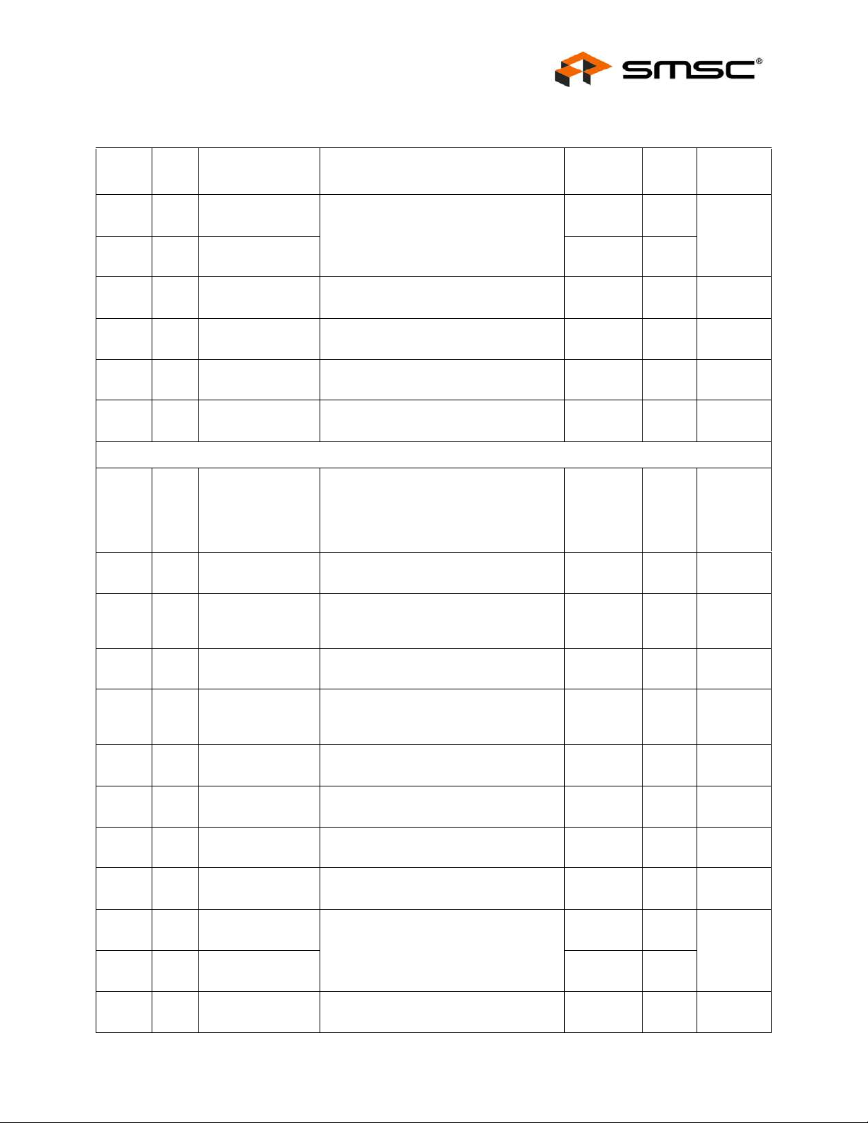
Table 5.1 EMC2305 Register Set (continued)
ADDR R/W
5Ah R/W
5Bh R/W
5Ch R/W
5Dh R/W
5Eh R
5Fh R
NAME FUNCTION
Fan 3 Drive Fail
Band Low Byte
Fan 3 Drive Fail
Band High Byte
TACH 3 Target
Low Byte
TACH 3 Target
High Byte
TACH 3 Reading
High Byte
TACH 3 Reading
Low Byte
60h R/W Fan 4 Setting
61h R/W PWM 4 Divi de
REGISTER
Stores the number of Tach counts used
to determine how the actual fan speed
must match the target fan speed at full
scale drive
Holds the target tachometer reading low
byte for Fan 3
Holds the target tachometer reading
high byte for Fan 3
Holds the tachometer reading high byte
for Fan 3
Holds the tachometer reading low byte
for Fan 3
Fan 4 Control Registers
Always displays the most recent fan
driver input setting for Fan 4. If the
RPM- based Fan Speed Control
Algorithm is disabled, allows direct user
control of the fan driver.
Stores the divide ratio to set the
frequency for Fan 4
DEFAULT
VALUE LOCK PAGE
00h SW L
Page 45
00h SW L
F8h No
FFh No
FFh No
F8h No
00h No
01h No
Page 46
Page 46
Page 47
Page 47
Page 36
Page 36
62h R/W
63h R/W
Fan 4
Configuration1
Fan 4
Configuration 2
65h R/W Gain 4
66h R/W
Fan 4 Spin Up
Configuration
67h R/W Fan 4 Max Step
68h R/W
69h R/W
6Ah R/W
6Bh R/W
6Ch R/W
Fan 4 Minimum
Drive
Fan 4 Valid TACH
Count
Fan 4 Drive Fail
Band Low Byte
Fan 4 Drive Fail
Band High Byte
TACH 4 Target
Low Byte
Sets configuration values for the RPM-
based Fan Speed Control Algorithm for
Fan 4
Sets additional configuration values for
the Fan 4 driver
Holds the gain terms used by the RPMbased Fan Speed Control Algorithm for
Fan 4
Sets the configuration values for Spin
Up Routine of the Fan 4 driver
Sets the maximum change per update
for Fan 4
Sets the minimum drive value for the
Fan 4 driver
Holds the tachometer reading that
indicates Fan 4 is spinning properly
Stores the number of Tach counts used
to determine how the actual fan speed
must match the target fan speed at full
scale drive
Holds the target tachometer setting low
byte for Fan 4
2Bh No
28h SW L
2Ah SWL
19h SW L
10h SW L
66h
(40%)
SWL
F5h SWL
00h SW L
00h SW L
F8h No
Page 37
Page 38
Page 40
Page 41
Page 43
Page 44
Page 44
Page 45
Page 46
SMSC EMC2305 29 Revision 1.3 (05-18-11)
DATASHEET
Page 30
Multiple RPM-Based PWM Fan Controller for Five Fans
Table 5.1 EMC2305 Register Set (continued)
Datasheet
ADDR R/W
6Dh R/W
6Eh R
6Fh R
NAME FUNCTION
TACH 4 Target
High Byte
TACH 4 Reading
High Byte
TACH 4 Reading
Low Byte
70h R/W Fan 5 Setting
71h R/W PWM 5 Divi de
REGISTER
72h R/W
73h R/W
Fan 5
Configuration1
Fan 5
Configuration 2
Holds the target tachometer setting high
byte for Fan 4
Holds the tachometer reading high byte
for Fan 4
Holds the tachometer reading low byte
for Fan 4
Fan 5 Control Registers
Always displays the most recent fan
driver input setting for Fan 5. If the
RPM- based Fan Speed Control
Algorithm is disabled, allows direct user
control of the fan driver.
Stores the divide ratio to set the
frequency for Fan 5
Sets configuration values for the RPM-
based Fan Speed Control Algorithm for
Fan 5
Sets additional configuration values for
the Fan 5 driver
DEFAULT
VALUE LOCK PAGE
FFh No
FFh No
F8h No
00h No
01h No
2Bh No
28h SW L
Page 46
Page 47
Page 47
Page 36
Page 36
Page 37
Page 38
75h R/W Gain 5
76h R/W
Fan 5 Spin Up
Configuration
77h R/W Fan 5 Max Step
78h R/W
79h R/W
7Ah R/W
7Bh R/W
7Ch R/W
7Dh R/W
7Eh R
Fan 5 Minimum
Drive
Fan 5 Valid TACH
Count
Fan 5 Drive Fail
Band Low Byte
Fan 5 Drive Fail
Band High Byte
TACH 5 Target
Low Byte
TACH 5 Target
High Byte
TACH 5 Reading
High Byte
Holds the gain terms used by the RPMbased Fan Speed Control Algorithm for
Fan 5
Sets the configuration values for Spin
Up Routine of the Fan 5 driver
Sets the maximum change per update
for Fan 5
Sets the minimum drive value for the
Fan 5 driver
Holds the tachometer reading that
indicates Fan 5 is spinning properly
Stores the number of Tach counts used
to determine how the actual fan speed
must match the target fan speed at full
scale drive
Holds the target tachometer setting low
byte for Fan 5
Holds the target tachometer setting high
byte for Fan 5
Holds the tachometer reading high byte
for Fan 5
2Ah SWL
19h SW L
10h SW L
66h
(40%)
SWL
F5h SWL
00h SW L
00h SW L
F8h No
FFh No
FFh No
Page 40
Page 41
Page 43
Page 44
Page 44
Page 45
Page 46
Page 46
Page 47
7Fh R
Revision 1.3 (05-18-11) 30 SMSC EMC2305
TACH 5 Reading
Low Byte
Holds the tachometer reading low byte
for Fan 5
F8h No
Page 47
DATASHEET
Page 31
Multiple RPM-Based PWM Fan Controller for Five Fans
Datasheet
Table 5.1 EMC2305 Register Set (continued)
ADDR R/W
REGISTER
NAME FUNCTION
DEFAULT
VALUE LOCK PAGE
Lock Register
EF R/W Software Lock Locks all SWL registers 00h SWL
Page 48
Revision Registers
FCh R Product Features
Indicates functions determined upon
device power up by external pin states
00h No
Page 48
FDh R Product ID Stores the unique Product ID 34h No Page 49
FEh R Manufacturer ID Stores the Manufacturer ID 5Dh No Page 50
FFh R Revision Revision 80h No Page 50
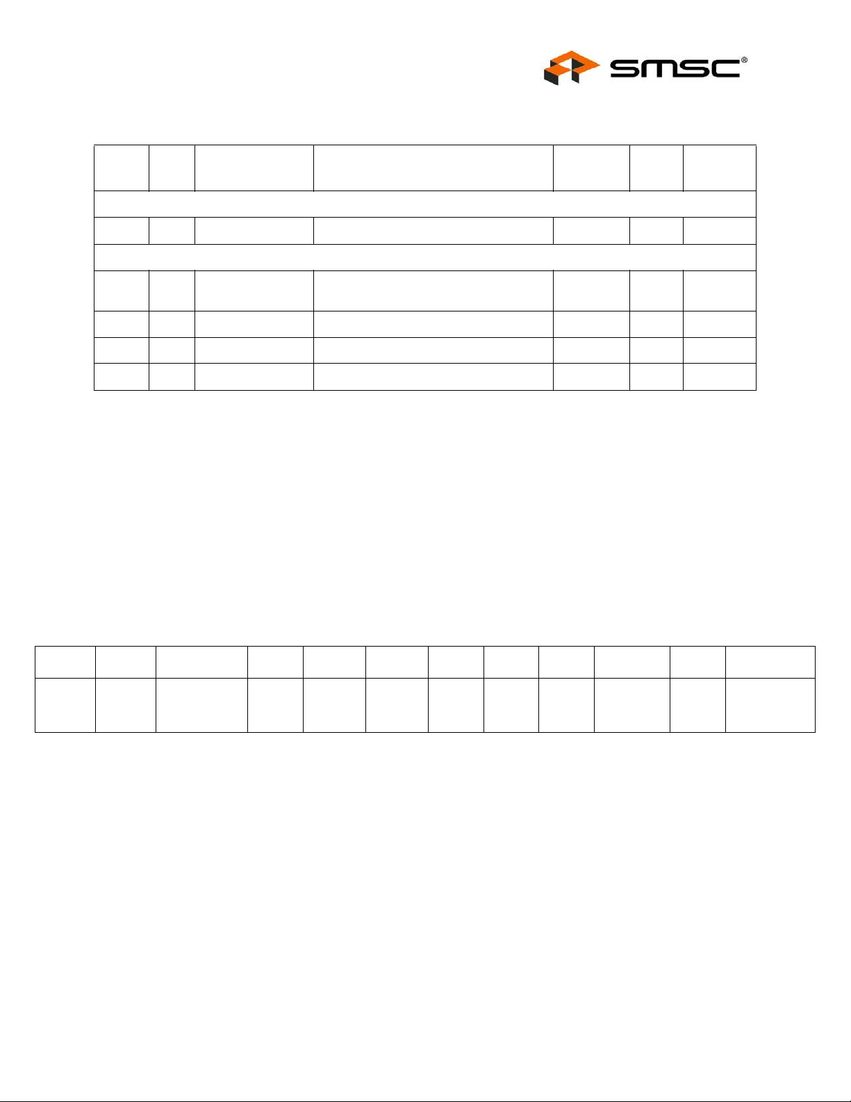
During Power-On-Reset (POR), the default values are stored in the registers. A POR is initiated when
power is first applied to the part and the voltage on the VDD supply surpasses the POR level as
specified in the electrical characteristics. Any reads to undefined registers will return 00h. Writes to
undefined registers will not have an effect.
5.1.1 Lock Entries
The Lock Column describes the locking mechanism, if any, used for individual registers. All SWL
registers are Software Locked and therefore made read-only when the LOCK bit is set.
5.2 Configuration Register
Table 5.2 Configuration Register
ADDR R/W REGISTER B7 B6 B5 B4 B3 B2 B1 B0 DEFAULT
USE_
EXT_
CLK
2
C compliant.
40h
20h R/W Configuration MASK DIS_TO WD_EN - - -
The Configuration Register controls the basic functionality of the EMC2305. The bits are described
below. The Configuration Register is software locked.
Bit 7 - MASK - Blocks the ALERT# pin from being asserted.
‘0’ (default) - The ALERT# pin is unmasked. If any bit in the status registers is set, the ALERT#
pin will be asserted (unless individually masked via the Fan Interrupt Enable Register).
‘1’ - The ALERT# pin is masked and will not be asserted.
Bit 6 - DIS_TO - Disables the SMBus timeout function for the SMBus client (if enabled).
‘0’ - The SMBus timeout function is enabled.
‘1’ (default) - The SMBus timeout function is disabled allowing the device to be fully I
Bit 5 - WD_EN - Enables the Watchdog timer (see
‘0’ (default) - The Watchdog timer does not operate continuously. It will function upon power up and
Section 4.8) to operate in Continuous Mode.
at no other time (see Section 4.8.1).
‘1’ - The Watchdog timer operates continuously as described in Section 4.8.2.
DR_EXT_
CLK
SMSC EMC2305 31 Revision 1.3 (05-18-11)
DATASHEET
Page 32

Multiple RPM-Based PWM Fan Controller for Five Fans
Datasheet
Bit 1 - DR_EXT_CLK - Enables the internal tachometer clock to be driven out on the CLK pin so that
multiple devices can be synced to the same source.
‘0’ (default) - The CLK pin acts as a clock input.
‘1’ - The CLK pin acts as a clock output and is a push-pull driver.
Bit 0 - USE_EXT_CLK - Enables the EMC2305 to use a clock present on the CLK pin as the
tachometer clock. If the DR_EXT_CLK bit is set, then this bit is ignored and the device will use the
internal oscillator.
‘0’ (default) - The EMC2305 will use its internal oscillator for all Tachometer measurements.
‘1’ - The EMC2305 will use the oscillator presented o n the CLK pin for all Tachometer
measurements.
5.3 Fan Status Registers
Table 5.3 Fan Status Registers
ADDR R/W REGISTER B7 B6 B5 B4 B3 B2 B1 B0 DEFAULT
24h R-C Fan Status WATCH - - - -
25h R-C
26h R-C
27h R-C
Fan Stall
Status
Fan Spin
Status
Fan Drive
Fail Status
---
---
---
FAN5_
STALL
FAN5_
SPIN
DRIVE_
FAIL5
FAN4_
STALL
FAN4_
SPIN
DRIVE_
FAI L4
The Fan Status registers contain the status bits associated with each fan driver.
5.3.1 Fan Status - 24h
The Fan Status register indicates that one or more of the fan drivers has stalled or failed or that the
Watchdog Timer has expired (see
Bit 7 - WATCH - Indicates that the Watchdog Timer has expired. When set, each fan is driven to 100%
duty cycle and will remain at 100% duty cycle until they are prog rammed. This bit is cleared when it
is read.
Bit 2 - DRIVE_FAIL - Indicates that one or more fan drivers cannot meet the programmed fan speed
at maximum PWM duty cycle. This bit is set when any bit in the Fan Drive Fail Status register is set
and cleared when all bits in the Fan Drive Fail Status register are cleared.
Bit 1 - FAN_SPIN - Indicates that one or more fan drivers cannot spin up. This bit is set when any bit
in the Fan Spin Status register is set and cleared when all of the bits in the Fan Spin Status register
are cleared.
Section 4.8).
DRIVE_
FAIL
FAN3_
STALL
FAN3_
SPIN
DRIVE_
FAIL3
FAN_
SPIN
FAN2_
STALL
FAN2_
SPIN
DRIVE_
FAIL2
FAN_
STALL
FAN1_
STALL
FAN1_
SPIN
DRIVE_
FAI L1
00h
00h
00h
00h
Bit 0 - FAN_STALL - Indicates that one or more fan drivers have stalled. This bit is set when any bit
in the Fan Stall Status register is set and cleared when all of the bits in the Fan Stall Status register
are cleared.
Revision 1.3 (05-18-11) 32 SMSC EMC2305
DATASHEET
Page 33

Multiple RPM-Based PWM Fan Controller for Five Fans
Datasheet
5.3.2 Fan Stall Status - 25h
The Fan Stall Status register indicates which fan driver has detected a stalled condition (see
Section 4.4.1). All bits are cleared upon a read if the error cond ition has been removed.
Bit 4 - FAN5_STALL - Indicates that Fan 5 has stalled.
Bit 3 - FAN4_STALL - Indicates that Fan 4 has stalled.
Bit 2 - FAN3_STALL - Indicates that Fan 3 has stalled.
Bit 1 - FAN2_STALL - Indicates that Fan 2 has stalled.
Bit 0 - FAN1_STALL - Indicates that Fan 1 has stalled.
5.3.3 Fan Spin Status - 26h
The Fan Spin Status register indicates which fan driver has failed to spin-up (see
are cleared upon a read if the error condition has been removed.
Bit 4 - FAN5_SPIN - Indicates that Fan 5 has failed to spin up.
Bit 3 - FAN4_SPIN - Indicates that Fan 4 has failed to spin up.
Bit 2 - FAN3_SPIN - Indicates that Fan 3 has failed to spin up.
Bit 1 - FAN2_SPIN - Indicates that Fan 2 has failed to spin up.
Bit 0 - FAN1_SPIN - Indicates that Fan 1 has failed to spin up.
5.3.4 Fan Drive Fail Status - 27h
The Fan Drive Fail Status register indicates which fan driver cannot drive to the programmed speed
even at 100% duty cycle (see
error condition has been removed.
Bit 4 - DRIVE_FAIL5 - Indicates that Fan 5 cannot reach its programmed fan speed even at 100% duty
cycle. This may be due to an aging fan or invalid programming.
Bit 3 - DRIVE_FAIL4 - Indicates that Fan 4 cannot reach its programmed fan speed even at 100% duty
cycle. This may be due to an aging fan or invalid programming.
Bit 2 - DRIVE_FAIL3 - Indicates that Fan 3 cannot reach its programmed fan speed even at 100% duty
cycle. This may be due to an aging fan or invalid programming.
Bit 1 - DRIVE_FAIL2 - Indicates that Fan 2 cannot reach its programmed fan speed even at 100% duty
cycle. This may be due to an aging fan or invalid programming.
Section 4.4.2 and Section 5.12). All bits are cleared upo n a read if the
Section 4.6). All bits
Bit 0 - DRIVE_FAIL1 - Indicates that Fan 1 cannot reach its programmed fan speed even at 100% duty
cycle. This may be due to an aging fan or invalid programming.
5.4 Fan Interrupt Enable Register
Table 5.4 Fan Interrupt Enable Register
ADDRR/WREGISTERB7B6B5B4 B3 B2 B1B0DEFAULT
29h R/W
SMSC EMC2305 33 Revision 1.3 (05-18-11)
Fan
Interrupt
Enable
---
DATASHEET
FAN5_
INT_EN
FAN4_
INT_EN
FAN3_
INT_EN
FAN2_
INT_EN
FAN1_
INT_EN
00h
Page 34
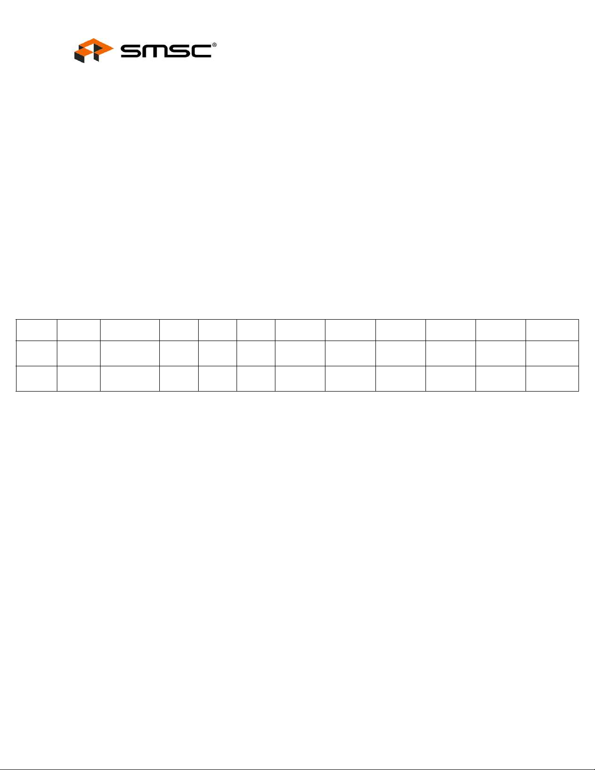
The Fan Interrupt Enable controls the masking for each Fan channel. When a channel i s enabled, it
will cause the ALERT# pin to be asserted when an error condition is detected .
Bit 4 - FAN5_INT_EN - Allows Fan 5 to assert the ALERT# pin if an error condition is detected.
Bit 3 - FAN4_INT_EN - Allows Fan 4 to assert the ALERT# pin if an error condition is detected.
Bit 2 - FAN3_INT_EN - Allows Fan 3 to assert the ALERT# pin if an error condition is detected.
Bit 1 - FAN2_INT_EN - Allows Fan 2 to assert the ALERT# pin if an error condition is detected.
Bit 0 - FAN1_INT_EN - Allows Fan 1 to assert the ALERT# pin if an error condition is detected.
‘0’ (default) - An error condition on Fan X will not cause the ALERT# pin to be asserted, however
the status registers will be updated normally.
‘1’ - An error condition (Stall, Spin Up, Drive Fail) on Fan X will cause the ALERT# pin to be
asserted.
5.5 PWM Configuration Registers
Table 5.5 PWM Configuration Registers
Multiple RPM-Based PWM Fan Controller for Five Fans
Datasheet
ADDR R/W REGISTER B7 B6 B5 B4 B3 B2 B1 B0 DEFAULT
2Ah R/W
2Bh R/W
PWM Polarity
Config
PWM Output
Config
---
- - - PWM5_OT PWM4_OT PWM3_OT PWM2_OT PWM1_OT 00h
POLARITY5POLARITY4POLARITY3POLARITY2POLARITY
1
00h
The PWM Config registers control the output type and polarity of all PWM outputs.
5.5.1 PWM Polarity Config - 2Ah
Bit 4 - POLARITY5 - Determines the polarity of PWM 5.
Bit 3 - POLARITY4 - Determines the polarity of PWM 4.
Bit 2 - POLARITY3 - Determines the polarity of PWM 3.
Bit 1 - POLARITY2 - Determines the polarity of PWM 2.
Bit 0 - POLARITY1 - Determines the polarity of PWM 1.
‘0’ (default) - the Polarity of the PWM driver is no rmal. A drive setting of 00h will cause the output
to be set at 0% duty cycle and a drive setting of FFh will cause the output to be set at 100% duty
cycle.
‘1’ - The Polarity of the PWM driver is inverted. A drive setting of 00h will cause the output to be
set at 100% duty cycle and a drive setting of FFh will cause the output to be set at 0% duty cycle.
5.5.2 PWM Output Config - 2Bh
Bit 4 - PWM5_OT - Determines the output type of the PWM 5 driver.
Bit 3 - PWM4_OT - Determines the output type of the of PWM 4 driver.
Bit 2 - PWM3_OT - Determines the output type of the of PWM 3 driver.
Bit 1 - PWM2_OT - Determines the output type of PWM 2 driver.
Revision 1.3 (05-18-11) 34 SMSC EMC2305
DATASHEET
Page 35
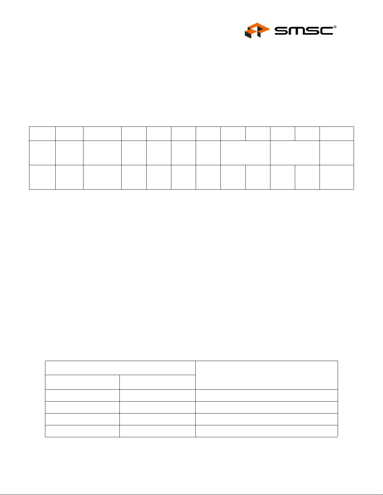
Multiple RPM-Based PWM Fan Controller for Five Fans
Datasheet
Bit 0 - PWM1_OT - Determines the output type of the PWM 1 driver.
‘0’ (default) - The PWM 1 output is configured as an open drain output.
‘1’ - The PWM 1 output is configured as a push-pull output.
5.6 PWM Base Frequency Registers
Table 5.6 PWM Base Frequency Registers
ADDRR/WREGISTERB7B6B5B4B3B2B1B0DEFAULT
PWM Base
2Ch R/W
2Dh R/W
Frequency
1
PWM Base
Frequency
2
The PWM Base Frequency registers determine the base frequency that is used with the PWM Divide
register to determine the final PWM frequency. Each PWM frequency is set by the base frequency and
its respective divide ratio (see
----
--
Section 5.8).
5.6.1 PWM Base Frequency 1 - 2Bh
Controls the base frequency of PWM drivers 4 and 5.
Bits 3-2 - PWM_BASE5[1:0] - Determines the base frequency of the PWM5 driver.
Bits 1-0 - PWM_BASE4[1:0] - Determines the base frequency of the PWM4 driver.
5.6.2 PWM Base Frequency 2 - 2Ch
Controls the base frequency of PWM drivers 1-3
Bits 5-6 - PWM_BASE3[1:0] - Determines the base frequency of the PWM3 driver.
Bits 3-2 - PWM_BASE2[1:0] - Determines the base frequency of the PWM2 driver.
PWM_
BASE
3_1
PWM_
BASE
3_0
PWM_BASE5
[1:0]
PWM_
BASE
2_1
PWM_
BASE
2_0
PWM_BASE4
[1:0]
PWM_
BASE
1_1
PWM_
BASE
00h
00h
1_0
Bits 1-0 - PWM_BASE1[1:0] - Determines the base frequency of the PWM1 driver.
Table 5.7 PWM_BASEx[1:0] Bit Decode
PWM_BASEX[1:0]
BASE FREQUENCY10
0 0 26.00kHz (default)
0 1 19.531kHz
1 0 4,882Hz
1 1 2,441Hz
SMSC EMC2305 35 Revision 1.3 (05-18-11)
DATASHEET
Page 36
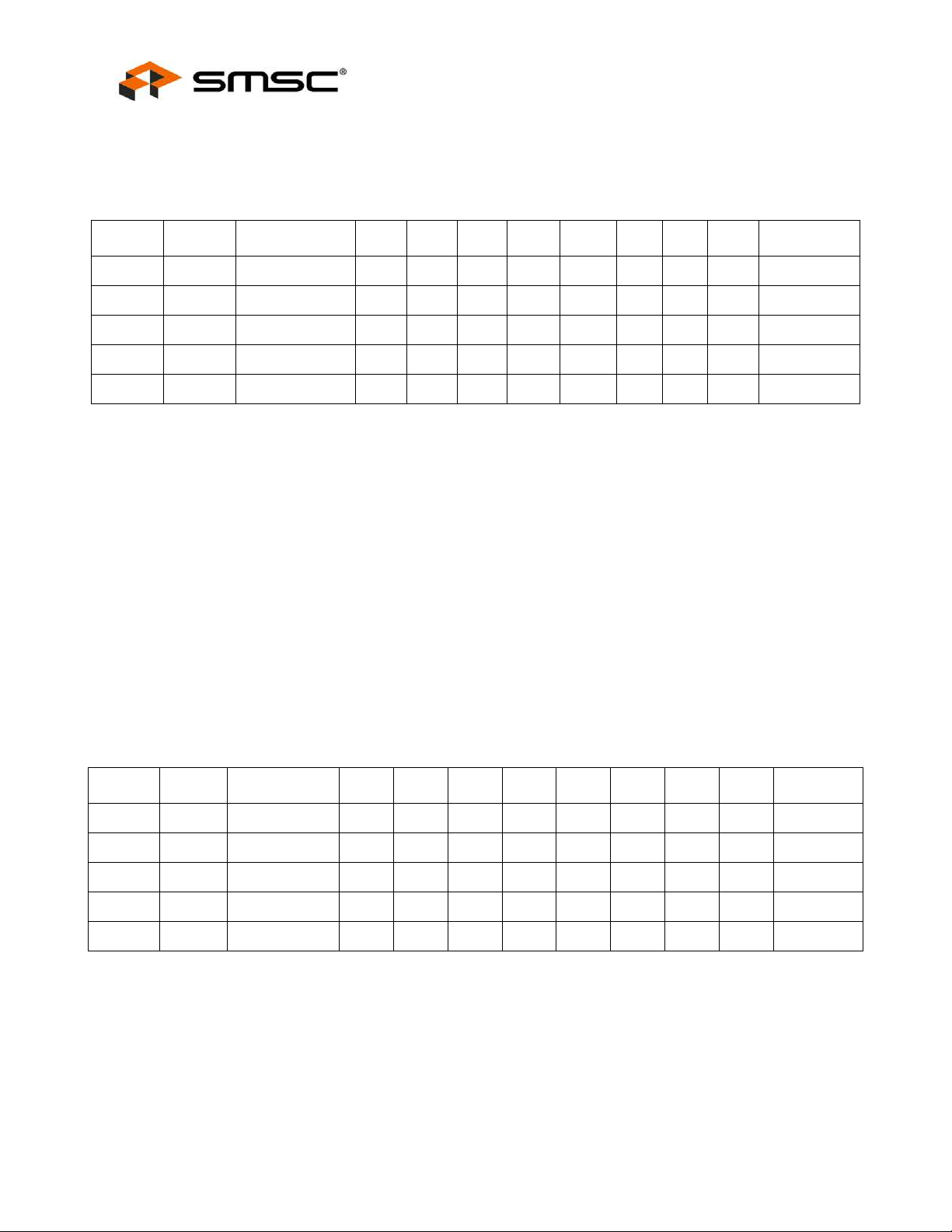
Multiple RPM-Based PWM Fan Controller for Five Fans
Drive
VALUE
255
-------------------- -
⎝⎠
⎛⎞
100%×=
Datasheet
5.7 Fan Setting Registers
Table 5.8 Fan Driver Setting Registers
ADDR R/W REGISTER B7 B6 B5 B4 B3 B2 B1 B0 DEFAULT
30h R/W Fan 1 Setting 128 64 32 16 8 4 2 1 00h
40h R/W Fan 2 Setting 128 64 32 16 8 4 2 1 00h
50h R/W Fan 3 Setting 128 64 32 16 8 4 2 1 00h
60h R/W Fan 4 Setting 128 64 32 16 8 4 2 1 00h
70h R/W Fan 5 Setting 128 64 32 16 8 4 2 1 00h
The Fan Setting register always displays the current setting of the respective fan driver. Reading from
any of the registers will report the current fan speed setting of the appropriate fan driver regardless of
the operating mode. Therefore it is possible that reading from this register will not report data that was
previously written into this register.
While the RPM-based Fan Speed Control Algorithm is active, the register is read only. Writing to the
register will have no effect and the data will not be stored.
The contents of the register represent the weighting of each bit in determining the final outp ut voltage.
The output drive for a PWM output is given by
Equation [1].
[1]
5.8 PWM Divide Registers
Table 5.9 PWM Divide Registers
ADDR R/W REGISTER B7 B6 B5 B4 B3 B2 B1 B0 DEFAULT
31h R/W Fan 1 Divide 128 64 32 16 8 4 2 1 01h
41h R/W Fan 2 Divide 128 64 32 1 6 8 4 2 1 01h
51h R/W Fan 3 Divide 128 64 32 16 8 4 2 1 01h
61h R/W Fan 4 Divide 128 64 32 1 6 8 4 2 1 01h
71h R/W Fan 5 Divide 128 64 32 16 8 4 2 1 01h
Revision 1.3 (05-18-11) 36 SMSC EMC2305
The PWM Divide registers determine the final frequency of the re spective PWM Fan Driver. Each driver
base frequency is divided by the value of the respec tive PWM Divide Register to determine the final
frequency. The duty cycle settings are not affected by these settings, only the final frequency of the
PWM driver. A value of 00h will be decoded as 01h.
DATASHEET
Page 37
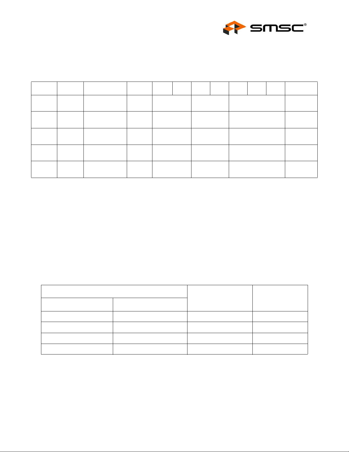
Multiple RPM-Based PWM Fan Controller for Five Fans
Datasheet
5.9 Fan Configuration 1 Registers
Table 5.10 Fan Configuration 1 Registers
ADDR R/W REGISTER B7 B6 B5 B 4 B3 B2 B1 B0 DEFAULT
32h R/W
42h R/W
52h R/W
62h R/W
72h R/W
Fan 1
Configuration 1
Fan 2
Configuration 1
Fan 3
Configuration 1
Fan 4
Configuration 1
Fan 5
Configuration 1
EN_
ALGO1
EN_
ALGO2
EN_
ALGO3
EN_
ALGO4
EN_
ALGO5
RANGE1[1:0] EDGES1[1:0] UPDATE1[2:0] 2Bh
RANGE2[1:0] EDGES2[1:0] UPDATE2[2:0] 2Bh
RANGE3[1:0] EDGES3[1:0] UPDATE3[2:0] 2Bh
RANGE4[1:0] EDGES4[1:0] UPDATE4[2:0] 2Bh
RANGE5[1:0] EDGES5[1:0] UPDATE5[2:0] 2Bh
The Fan Configuration 1 registers control the general operation of the RPM-based Fan Speed Control
Algorithm used for the respective Fan Driver.
Bit 7 - EN_ALGOx - enables the RPM-based Fan Speed Control Algorithm.
‘0’ - (default) the control circuitry is disabled and the fan dri ver output is determined by the Fan
Driver Setting Register.
‘1’ - the control circuitry is enabled and the Fan Driver outp ut will be automatically updated to
maintain the programmed fan speed as indicated by the TACH Target Register.
Bits 6- 5 - RANGEx[1:0] - Adjusts the range of reported and programmed tachometer reading values.
The RANGE bits determine the weighting of all TACH values (including the Valid TACH Count, TACH
Target, and TACH reading) as shown in
Table 5.11.
Table 5.11 Range Decode
RANGEX[1:0]
REPORTED MINIMUM
RPM
TACH COUNT
MULTIPLIER10
005001
0 1 1000 (default) 2
1 0 2000 4
1 1 4000 8
Bits 4-3 - EDGESx[1:0] - determines the minimum number of edges that must be detected on the
TACHx signal to determine a single rotation. A typical fan measured 5 ed ges (for a 2-pole fan). For
more accurate tachometer measurement, the minimum number of edges measured may be incre ased.
Increasing the number of edges measured with respect to th e number of poles of the fan will cause
the TACH Reading registers to indicate a fan speed that is higher or lower than the actual speed. In
order for the FSC Algorithm to operate correctly, the TACH Target must be updated by the user to
accommodate this shift. The Effective Tach Multiplier shown in
Table 5.12 is used as a direct multiplier
term that is applied to the Actual RPM to achieve the Reported RPM. It should only be applied if the
SMSC EMC2305 37 Revision 1.3 (05-18-11)
DATASHEET
Page 38
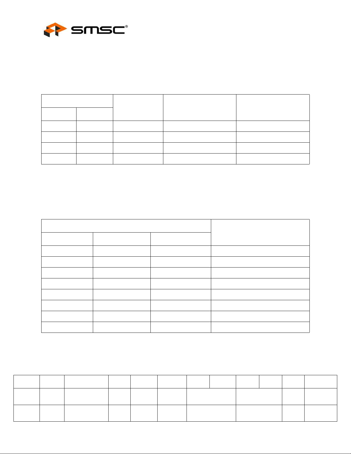
Multiple RPM-Based PWM Fan Controller for Five Fans
Datasheet
number of edges measured does not match the number of edges expected based on the number of
poles of the fan (which is fixed for any given fan).
Contact SMSC for recommended settings when using fans with more or less than 2 poles.
Table 5.12 Minimum Edges for Fan Rotation
EDGESX[1:0]
MINIMUM TACH
EDGES NUMBER OF FAN POLES
0 0 3 1 pole 0.5
0 1 5 2 poles (default) 1
1 0 7 3 poles 1.5
1 1 9 4 poles 2
Bit 2-0 - UPDATEx[2:0] - determines the base time between fan driver updates. The Update Time,
along with the Fan Step Register, is used to control the ramp rate of the drive response to provide a
cleaner transition of the actual fan operation as the desired fan speed changes. The Update Time is
set as shown in
00 0 100ms
00 1 200ms
Table 5.13.
Table 5.13 Update Time
UPDA TEX[2:0]
EFFECTIVE TACH
MULTIPLIER (BASED ON 2
POLE FANS)10
UPDATE TIME 21 0
01 0 300ms
0 1 1 400ms (default)
10 0 500ms
10 1 800ms
1 1 0 1200ms
1 1 1 1600ms
5.10 Fan Configuration 2 Registers
Table 5.14 Fan Configuration 2 Registers
ADDR R/W REGISTER B7 B6 B5 B4 B3 B2 B1 B0 DEFAULT
33h R/W
43h R/W
Revision 1.3 (05-18-11) 38 SMSC EMC2305
Fan 1
Configuration 2
Fan 2
Configuration 2
-
-
EN_
RRC1
EN_
RRC2
GLITCH_
EN1
GLITCH_
EN2
DATASHEET
DER_OPT1 [1:0] ERR_RNG1[1:0] - 28h
DER_OPT2 [1:0] ERR_RNG2[1:0] - 28h
Page 39
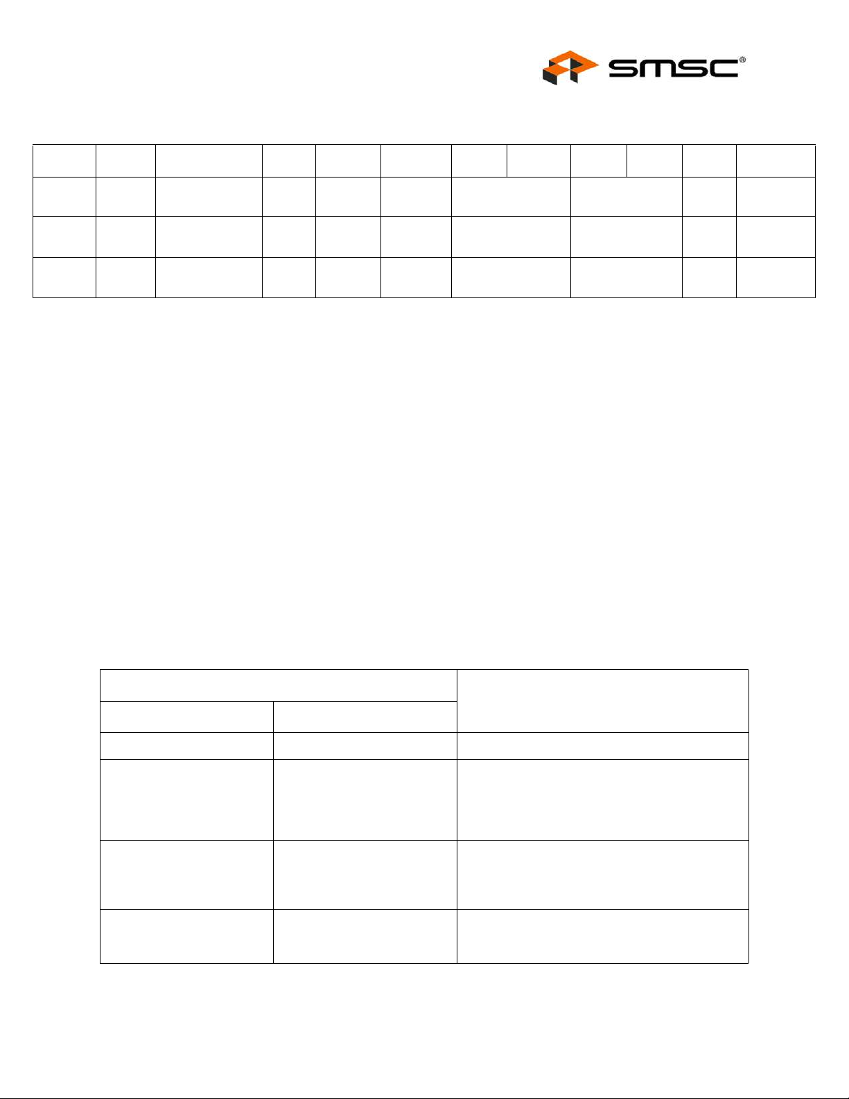
Multiple RPM-Based PWM Fan Controller for Five Fans
Datasheet
Table 5.14 Fan Configuration 2 Registers (continued)
ADDR R/W REGISTER B7 B6 B5 B4 B3 B2 B1 B0 DEFAULT
53h R/W
63h R/W
73h R/W
Fan 3
Configuration 2
Fan 4
Configuration 2
Fan 5
Configuration 2
-
-
-
EN_
RRC3
EN_
RRC4
EN_
RRC5
GLITCH_
EN3
GLITCH_
EN4
GLITCH_
EN5
DER_OPT3 [1:0] ERR_RNG3[1:0] - 28h
DER_OPT4 [1:0] ERR_RNG4[1:0] - 28h
DER_OPT5 [1:0] ERR_RN55[1:0] - 28h
The Fan Configuration 2 registers control the tachometer measurement and advanced features of the
RPM-based Fan Speed Control Algorithm.
Bit 6 - EN_RRCx - Enables ramp rate control when the corresponding fan driver is operated in the
Direct Setting Mode.
‘0’ (default) - Ramp rate control is disabled. When the fan driver is operating in Direct Setting mode,
the fan setting will instantly transition to the next programmed setting.
‘1’ - Ramp rate control is enabled. When the fan driver is opera ting in Direct Setting mode, the fan
drive setting will follow the ramp rate controls as determined by the Fan Step and Update Time
settings. The maximum fan drive setting step is capped at the Fa n Step setting and is updated
based on the Update Time as given by
Table 5.13.
Bit 5 - GLITCH_ENx - Disables the low pass glitch filter that removes high frequency noise injected
on the TACHx pin.
‘0’ - The glitch filter is disabled.
‘1’ (default) - The glitch filter is enabled.
Bits 4 - 3 - DER_OPTx[1:0] - Control some of the advan ced options that affect the derivative portion
of the RPM-based Fan Speed Control Algorithm as shown in
Table 5.15.
Table 5.15 Derivative Option s
DER_OPTX[1:0]
OPERATION10
0 0 No derivative options used
Basic derivative. The derivative of the error from
the current drive setting and the target is added
01
to the iterative Fan Drive Register setting (in
addition to proportional and integral terms)
(default)
Step derivative. The derivative of the error from
10
the current drive setting and the target is added
to the iterative Fan Drive Register setting and is
not capped by the Fan Step Register.
Both the basic derivative and the step derivative
11
are used effectively causing the derivative term to
have double the effect of the derivative term.
Bit 2 - 1 - ERR_RNGx[1:0] - Control some of the advanced options that affect the error window. When
the measured fan speed is within the programmed error windo w around the target speed, th en the fan
SMSC EMC2305 39 Revision 1.3 (05-18-11)
DATASHEET
Page 40
drive setting is not updated. The algorithm will continue to monitor the fan speed and calculate
necessary drive setting changes based on the error; however, these changes are ignored.
ERR_RNGX[1:0]
0 0 0 RPM (default)
0 1 50 RPM
1 0 100 RPM
1 1 200 RPM
5.11 Gain Registers
Multiple RPM-Based PWM Fan Controller for Five Fans
Datasheet
Table 5.16 Error Range Options
OPERATION10
Table 5.17 Gain Registers
ADDR R/W REGISTER B7 B6 B5 B4 B3 B2 B1 B0 DEFAULT
35h R/W
45h R/W
55h R/W
65h R/W
75h R/W
Gain 1
Register
Gain 2
Register
Gain 3
Register
Gain 4
Register
Gain 5
Register
The Gain registers store the gain terms used by the proporti onal and integral portions of each of the
RPM-based Fan Speed Control Algorithms. These gain terms are used as the KD, KI, and KP gain
terms in a classic PID control solution.
Bits 5 - 4 - GAINDX[1:0] - Controls the derivative gain term used by the FSC algorithm as shown in
Table 5.18.
Bits 3-2 - GAINIX[1:0] - Controls the integral gain term used by the FSC algorithm as shown in
Table 5.18.
- - GAIND1[1:0] GAINI1[1:0] GAINP1[1:0] 2Ah
- - GAIND2[1:0] GAINI2[1:0] GAINP2[1:0] 2Ah
- - GAIND3[1:0] GAINI3[1:0] GAINP3[1:0] 2Ah
- - GAIND4[1:0] GAINI4[1:0] GAINP4[1:0] 2Ah
- - GAIND5[1:0] GAINI5[1:0] GAINP5[1:0] 2Ah
Bits 1-0 - GAINP[1:0] - Controls the proportional gain term used by the FSC algorithm as shown in
Table 5.18.
Revision 1.3 (05-18-11) 40 SMSC EMC2305
DATASHEET
Page 41
Multiple RPM-Based PWM Fan Controller for Five Fans
Datasheet
Table 5.18 Gain Decode
GAIND OR GAINP OR GAINI [1:0]
RESPECTIVE GAIN FACTOR10
00 1x
01 2x
1 0 4x (default)
11 8x
5.12 Fan Spin Up Configuration Registers
Table 5.19 Fan Spin Up Configuration Registers
ADDR R/W REGISTER B7 B6 B5 B4 B3 B2 B1 B0 DEFAULT
36h R/W
46h R/W
56h R/W
66h R/W
76h R/W
Fan 1 Spin Up
Configuration
Fan 2 Spin up
Configuration
Fan 3 Spin up
Configuration
Fan 4 Spin up
Configuration
Fan 5 Spin up
Configuration
The Fan Spin Up Configuration registers control the settings of Spin Up Routine. The Fan Spin Up
Configuration registers are software locked.
Bit 7 - 6 - DRIVE_FAIL_CNTx[1:0] - Determines how many update cycles are used for the Drive Fail
detection function as shown in
the desired tach target.
DRIVE_FAIL_CNTX[1:0]
DRIVE_FAIL_
CNT1 [1:0]
DRIVE_FAIL_
CNT2 [1:0]
DRIVE_FAIL_
CNT3 [1:0]
DRIVE_FAIL_
CNT4 [1:0]
DRIVE_FAIL_
CNT5 [1:0]
Table 5.20 DRIVE_FAIL_CNT[1:0] Bit Decode
NOKICK1 SPIN_LVL1[2:0]
NOKICK2 SPIN_LVL2[2:0]
NOKICK3 SPIN_LVL3[2:0]
NOKICK4 SPIN_LVL4[2:0]
NOKICK5 SPIN_LVL5[2:0]
Table 5.20. This circuitry determines whether th e fan can be driven to
SPINUP_TIME
1 [1:0]
SPINUP_TIME
2 [1:0]
SPINUP_TIME
3[1:0]
SPINUP_TIME
4 [1:0]
SPINUP_TIME
5 [1:0]
19h
19h
19h
19h
19h
NUMBER OF UPDATE PERIODS10
0 0 Disabled - the Drive Fail detection circuitry is disabled (default)
01
SMSC EMC2305 41 Revision 1.3 (05-18-11)
16 - the Drive Fail detection circuitry will count for 16 update
periods
DATASHEET
Page 42
Table 5.20 DRIVE_FAIL_CNT[1:0] Bit Decode (continued)
DRIVE_FAIL_CNTX[1:0]
Multiple RPM-Based PWM Fan Controller for Five Fans
Datasheet
NUMBER OF UPDATE PERIODS10
10
11
32 - the Drive Fail detection circuitry will count for 32 update
periods
64 - the Drive Fail detection circuitry will count for 64 update
periods
Bit 5 - NOKICKx - Determines if the Spin Up Routine will drive the fan to 100% duty cycle for 1/4 of
the programmed spin up time before driving it at the programmed level.
‘0’ (default) - The Spin Up Routine will drive the fan driver to 100% for 1/4 of the programme d spin
up time before reverting to the programmed spin level.
‘1’ - The Spin Up Routine will not drive the fan driver to 100%. It will set the drive at the
programmed spin level for the entire duration of the programmed spin up time.
Bits 4 - 2 - SPIN_LVLx[2:0] - Determines the final drive level that is used by the Spin Up Routine as
shown in Table 5.21.
Table 5.21 Spin Level
SPIN_LVLX[2:0]
SPIN UP DRIVE LEVEL210
0 0 0 30%
0 0 1 35%
0 1 0 40%
0 1 1 45%
1 0 0 50%
1 0 1 55%
1 1 0 60% (default)
1 1 1 65%
Bit 1 -0 - SPINUP_TIMEx[1:0] - determines the maximum Spin Time that the Spin Up Routine will run
for (see
Section 4.6). If a valid tachometer measurement is not detected before the Spin Time has
elapsed, an interrupt will be generated. When the RPM-bas ed Fan Speed Control Algorithm is active,
the fan driver will attempt to re-start the fan immediately after the end of the last spin up attempt.
The Spin Time is set as shown in
Table 5.22.
Revision 1.3 (05-18-11) 42 SMSC EMC2305
DATASHEET
Page 43
Multiple RPM-Based PWM Fan Controller for Five Fans
Datasheet
Table 5.22 Spin Time
SPINUP_TIMEX[1:0]
0 0 250 ms
0 1 500 ms (default)
1 0 1 sec
1 1 2 sec
5.13 Fan Max Step Registers
Table 5.23 Fan Max Step Registers
TOT A L SP I N U P TI M E10
ADDR R/W REGISTER B7 B6 B5 B4 B3 B2 B1 B0 DEFAULT
37h R/W
47h R/W
57h R/W
67h R/W
77h R/W
The Fan Max Step registers, along with the Update Time, control the ramp rate of the fan driver
response calculated by the RPM-based Fan Speed Control Algorithm. The value of the register
represents the maximum step size each fan driver will take between update times (see
When the FSC algorithm is enabled, Ramp Rate control is automatically used. When the FSC is not
active, then Ramp Rate control can be enabled by asserting the EN_RRC bit (see
APPLICATION NOTE: The UPDATE bits and Fan Step Register settin gs operate independently of the RPM-based
Fan 1 Max
Step
Fan 2 Max
Ste p
Fan 3 Max
Ste p
Fan 4 Max
Ste p
Fan 5 Max
Ste p
Fan Speed Control Algorithm and will always limit the fan drive setting. That is, if the
programmed fan drive setting (either as determined by the RPM-based F an Speed Control
Algorithm or by manual settings) exceeds the current fan drive setting by greater than the
Fan Step Register setting, the EMC2305 will limit the fan drive change to the value of the
Fan Step Register. It will use the Update Time to determine how often to update the drive
settings.
- - 32 16 8 4 2 1 10h
- - 32 16 8 4 2 1 10h
- - 32 16 8 4 2 1 10h
- - 32 16 8 4 2 1 10h
- - 32 16 8 4 2 1 10h
Section 5.9).
Section 5.10).
APPLICATION NOTE: If the Fan Speed Control Algorithm is used, the default settings in the Fan Configuration 2
Register will cause the maximum fan step settings to be ignored.
The Fan Max Step registers are software locked.
SMSC EMC2305 43 Revision 1.3 (05-18-11)
DATASHEET
Page 44
Multiple RPM-Based PWM Fan Controller for Five Fans
Datasheet
5.14 Fan Minimum Drive Registers
Table 5.24 Minimum Fan Drive Registers
ADDRR/WREGISTERB7B6B5B4B3B2B1B0DEFAULT
38h R/W
48h R/W
58h R/W
68h R/W
78h R/W
Fan 1
Minimum
Drive
Fan 2
Minimum
Drive
Fan 3
Minimum
Drive
Fan 4
Minimum
Drive
Fan 5
Minimum
Drive
The Fan Minimum Drive registers store the minimum drive setting for each RPM-based Fan Speed
Control Algorithm. The RPM-based Fan Speed Control Algorithm will not drive the fan at a level lower
than the minimum drive unless the target Fan Speed is set at FFh (see
During normal operation, if the fan stops for any reason (including low drive), the RPM-based Fan
Speed Control Algorithm will attempt to restart the fan. Setting the Fan Minimum Dri ve Register to a
setting that will maintain fan operation is a useful way to avoid potential fan oscillations as the control
circuitry attempts to drive it at a level that cannot support fan operation.
128643216 8 4 2 1
128643216 8 4 2 1
128643216 8 4 2 1
128643216 8 4 2 1
128643216 8 4 2 1
Section 5.17).
66h
(40%)
66h
(40%)
66h
(40%)
66h
(40%)
66h
(40%)
The Fan Minimum Drive Registers are software locked.
5.15 Valid TACH Count Registers
Table 5.25 Valid TACH Count Registers
ADDRR/WREGISTERB7B6B5B4B3B2B1B0DEFAULT
39h R/W
49h R/W
59h R/W
69h R/W
79h R/W
Revision 1.3 (05-18-11) 44 SMSC EMC2305
Valid TACH
Count 1
Valid TACH
Count 2
Valid TACH
Count 3
Valid TACH
Count 4
Valid TACH
Count 5
4096 2048 1024 512 256 128 64 32 F5h
4096 2048 1024 512 256 128 64 32 F5h
4096 2048 1024 512 256 128 64 32 F5h
4096 2048 1024 512 256 128 64 32 F5h
4096 2048 1024 512 256 128 64 32 F5h
DATASHEET
Page 45
Multiple RPM-Based PWM Fan Controller for Five Fans
Datasheet
The Valid TACH Count registers store the maximum TACH Reading Register value to indicate that
each fan is spinning properly. The value is referenced at the end of the Spin Up Routine to determine
if the fan has started operating and decide if the device needs to retry. See
for translating the count to an RPM.
If the TACH Reading Register value exceeds the Valid TACH Count Register (indicating that the Fan
RPM is below the threshold set by this count), then a stalled fan is detected. In this condition, the
algorithm will automatically begin its Spin Up Routine.
If a TACH Target setting is set above the Valid TACH Count setting, then that setting will be ignored
and the algorithm will use the current fan drive setting.
The Valid TACH Count registers are software locked.
Equation [2] in Section 5.18
5.16 Fan Drive Fail Band Registers
Table 5.26 Fan Drive Fail Band Registers
ADDR R/W REGISTER B7 B6 B5 B4 B3 B2 B1 B0 DEFAULT
Fan 1 Drive
3Ah R/W
Fail Band
Low Byte
16 8 4 2 1 - - - 00h
3Bh R/W
4Ah R/W
4Bh R/W
5Ah R/W
5Bh R/W
6Ah R/W
6Bh R/W
7Ah R/W
Fan 1 Drive
Fail Band
High Byte
Fan 2 Drive
Fail Band
Low Byte
Fan 2 Drive
Fall Band
High Byte
Fan 3 Drive
Fail Band
Low Byte
Fan 3 Drive
Fail Band
High Byte
Fan 4 Drive
Fail Band
Low Byte
Fan 4 Drive
Fall Band
High Byte
Fan 5 Drive
Fail Band
Low Byte
4096 20 48 102 4 512 256 128 64 32 00h
16 8 4 2 1 - - - 00h
4096 20 48 102 4 512 256 128 64 32 00h
16 8 4 2 1 - - - 00h
4096 20 48 102 4 512 256 128 64 32 00h
16 8 4 2 1 - - - 00h
4096 20 48 102 4 512 256 128 64 32 00h
16 8 4 2 1 - - - 00h
Fan 5 Drive
7Bh R/W
SMSC EMC2305 45 Revision 1.3 (05-18-11)
Fall Band
High Byte
4096 20 48 102 4 512 256 128 64 32 00h
DATASHEET
Page 46

Multiple RPM-Based PWM Fan Controller for Five Fans
Datasheet
The Fan Drive Fail Band Registers store the number of tach counts used by the Fan Drive Fail
detection circuitry. This circuitry is activated when the fan drive setting high byte is at FFh. When it is
enabled, the actual measured fan speed is compared against the target fan speed. T hese registers
are only used when the FSC is active.
This circuitry is used to indicate that the target fan speed at full dri ve is higher than the fan is actually
capable of reaching. If the measured fan speed does not exceed the target fan speed minus the Fan
Drive Fail Band Register settings for a period of time longer than set by the DRIVE_FAIL_CNTx[1:0]
bits, then the DRIVE_FAIL status bit will be set and an interrupt generated.
5.17 TACH Target Registers
Table 5.27 TACH Target Registers
ADDR R/W REGISTER B7 B6 B5 B4 B3 B2 B1 B0 DEFAULT
3Ch R/W
3Dh R/W
4Ch R
4Dh R/W
5Ch R
5Dh R/W
6Ch R
6Dh R/W
7Ch R
7Dh R/W
TACH Target
1 Low Byte
T ACH Target
1 High Byte
TACH Target
2 Low Byte
TACH Target
2 High Byte
TACH Target
3 Low Byte
TACH Target
3 High Byte
TACH Target
4 Low Byte
TACH Target
4 High Byte
TACH Target
5 Low Byte
TACH Target
5 High Byte
168421-- - F8h
4096 20 48 102 4 512 256 128 64 32 FFh
168421-- - F8h
4096 20 48 102 4 512 256 128 64 32 FFh
168421-- - F8h
4096 20 48 102 4 512 256 128 64 32 FFh
168421-- - F8h
4096 20 48 102 4 512 256 128 64 32 FFh
168421-- - F8h
4096 20 48 102 4 512 256 128 64 32 FFh
The TACH Target Registers hold the target tachometer value that is maintained by the RPM-based
Fan Speed Control Algorithm.
The value in the TACH Target Registers will always reflect the current TACH Target value.
If one of the algorithms is enabled, setting the TACH Target Register to FFh will disa ble the fan driver
(set the fan drive setting to 0%). Setting the TACH Target to any other value (from a setting of FFh)
will cause the algorithm to invoke the Spin Up Routine after which it will function normally.
The Tach Target is not applied until the high byte is written. Once th e high byte is written, the current
value of both high and low bytes will be used as the next Tach target.
Revision 1.3 (05-18-11) 46 SMSC EMC2305
DATASHEET
Page 47

Multiple RPM-Based PWM Fan Controller for Five Fans
Datasheet
5.18 TACH Reading Registers
Table 5.28 TACH Reading Registers
ADDR R/W REGISTER B7 B6 B5 B4 B3 B2 B1 B0 DEFAULT
3Eh R Fan 1 TACH 4096 2048 1024 512 256 128 64 32 FFh
3Fh R
4Eh R Fan 2 TACH 4096 2048 1024 512 256 128 64 32 FFh
4Fh R
5Eh R Fan 3 TACH 4096 2048 1024 512 256 128 64 32 FFh
5Fh R
6Eh R Fan 4 TACH 4096 2048 1024 512 256 128 64 32 FFh
6Fh R
7Eh R Fan 5 TACH 4096 2048 1024 512 256 128 64 32 FFh
7Fh R
The TACH Reading Registers’ contents describe the current tachometer reading for each of the fans.
By default, the data represents the fan speed as the number of 32kHz clock periods that occur for a
single revolution of the fan.
Equation [2] shows the detailed conversion from TACH measurement (COUNT) to RPM while Equation
[3]
measuring 5 edges, with a frequency of 32.768kHz. These equations are solved and tabulated for ease
of use in
Fan 1 TACH
Low Byte
Fan 2 TACH
Low Byte
Fan 3 TACH
Low Byte
Fan 4 TACH
Low Byte
Fan 5 TACH
Low Byte
shows the simplified translation of TACH Reading Register count to RPM assuming a 2-pole fan,
AN17.4 RPM to TACH Counts Conversion.
168421-- - F8h
168421-- - F8h
168421-- - F8h
168421-- - F8h
168421-- - F8h
Whenever the high byte register is read, the corresponding low byte data will be loaded to internal
shadow registers so that when the low byte is read, the da ta will always coincide with the previously
read high byte.
SMSC EMC2305 47 Revision 1.3 (05-18-11)
DATASHEET
Page 48
Multiple RPM-Based PWM Fan Controller for Five Fans
RPM
1
poles()
--------------------
n 1–()
COUNT
1
m
---- -
×
--------------------------------- -
f
TACH
60×××=
RPM
3,932,160 m×
COUNT
--------------------------------------
=
Datasheet
where:
poles = number of poles of the fan
(typically 2)
= the tachometer
f
TAC H
measurement frequency (typically
[2]
32.768kHz)
n = number of edges measured
(typically 5 for a 2 pole fan)
m = the multiplier defined by the
RANGE bits
[3]
COUNT = TACH Reading Register
value (in decimal)
5.19 Software Lock Register
Table 5.29 Software Lock Register
ADDR R/W REGISTER B7 B6 B5 B4 B3 B2 B1 B0 DEFA ULT
EFh R/W
Software
Lock
-------LOCK00h
The Software Lock Register controls the software locking of critical registers. This register is software
locked.
Bit 0 - LOCK - this bit acts on all registers that are designated SWL. When this bi t is set, the locked
registers become read only and cannot be updated.
‘0’ (default) - all SWL registers can be updated normally.
‘1’ - all SWL registers cannot be updated and a hard-reset is required to unlock them.
5.20 Product Features Register
Table 5.30 Product Features Register
ADDRESS R/W REGISTER B7 B6 B5 B4 B3 B2 B1 B0 DEFAULT
FCh R
The Product Features register shows those functions that are enabled by external pin states.
Bits 5-3 - ADR[2:0] - Indicates the selected SMBus address as determined by the ADDR_SEL pin.
Product
Features
- - ADR[2:0] FAN_SPD [2:0] 00h
Revision 1.3 (05-18-11) 48 SMSC EMC2305
DATASHEET
Page 49
Multiple RPM-Based PWM Fan Controller for Five Fans
Datasheet
Table 5.31 ADDR_SEL Pin Configuration
ADR[2:0]
21 0
0 0 0 0101_110(r/w)
0 0 1 0101_111(r/w)
0 1 0 0101_100(r/w)
0 1 1 0101_101(r/w)
1 0 0 1001_100(r/w)
1 0 1 1001_101(r/w)
Bits 2-0 - FAN_SPD[2:0] - Indicates the selected fan speed if the CLK pin pull-up decode is enabled
via the ADDR_SEL pin.
SLAVE ADDRESS
Table 5.32 FAN_SPD Pin Configuration
FAN_SPD [2:0]
FAN SPEED
21 0
0 0 0 0% Drive
0 0 1 30% Drive
0 1 0 50% Drive
0 1 1 75% Drive
1 0 0 100% Drive
5.21 Product ID R egister
Table 5.33 Product ID Register
ADDR R/W REGISTER B7 B6 B5 B4 B3 B2 B1 B0 DEFAULT
FDh R Product ID 0 0 1 1 0 1 0 0 34h
The Product ID Register contains a unique 8-bit word that identifies th e product.
SMSC EMC2305 49 Revision 1.3 (05-18-11)
DATASHEET
Page 50
Multiple RPM-Based PWM Fan Controller for Five Fans
Datasheet
5.22 Manufacturer ID Register
Table 5.34 Manufacturer ID Register
ADDR R/W REGISTER B7 B6 B5 B4 B3 B2 B1 B0 DEFAULT
FEh R Manufacturer ID 0 1 0 1 1 1 0 1 5Dh
The Manufacturer ID Register contains an 8-bit word that identifies SMSC.
5.23 Revision Register
Table 5.35 Revision Register
ADDR R/W REGISTER B7 B6 B5 B4 B3 B2 B1 B0 DEFAULT
FFh R Revision 1 0 0 0 0 0 0 0 80h
The Revision Register contains an 8-bit word that identifies the die revision .
Revision 1.3 (05-18-11) 50 SMSC EMC2305
DATASHEET
Page 51
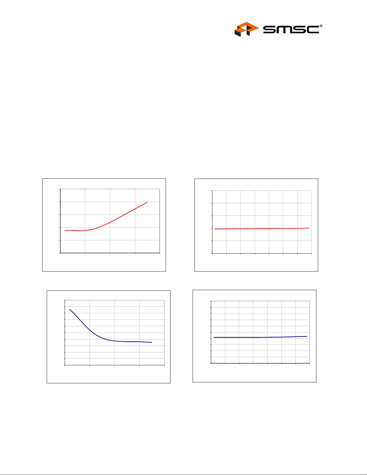
Multiple RPM-Based PWM Fan Controller for Five Fans
Supply Current vs. Ambient Temperature
500
550
600
650
700
750
-50 0 50 100 150
Temperature (C)
Supply Current (uA)
Supply Current (uA)
Ambient Temperature (°C)
Supply Current vs. Supply Voltage
500
550
600
650
700
750
2.95 3.05 3.15 3.25 3.35 3.45 3.55 3.65
Supply Voltage (V)
Supply Current (uA)
Supply Voltage (V)
Tachometer Measurement Accuracy vs. Ambient Temperature
-1
-0.8
-0.6
-0.4
-0.2
0
0.2
0.4
0.6
0.8
1
-50 0 50 100 150
Temperautre (C)
Ambient Temperature (°C)
Tach Measurement Accuracy (%)
Tachometer M easurement Accuracy vs. Supply Voltage
-1
-0.8
-0.6
-0.4
-0.2
0
0.2
0.4
0.6
0.8
1
2.95 3.05 3.15 3.25 3.35 3.45 3.55 3.65
Supply Voltage (V)
Tach Measurement Accuracy (%)
Datasheet
Chapter 6 Typical Operating Curves
The following Typical Operating Curves are included.
Supply Current vs. Temperature
Supply Current vs. Supply Voltage
Fan TACH Accuracy vs. Temperature
Fan TACH Accuracy vs. Supply Voltage
PWM output frequency vs. Supply Voltage
PWM output frequency vs. Temperature
FSC Operation
Tach Measurement Accuracy (%
SMSC EMC2305 51 Revision 1.3 (05-18-11)
Supply Current (uA)
Tach M easurement Accuracy (%
DATASHEET
Page 52
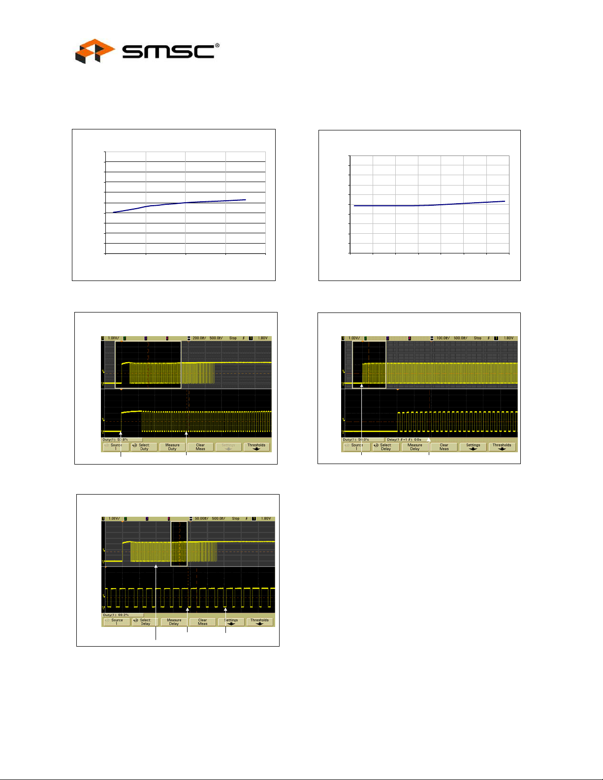
Multiple RPM-Based PWM Fan Controller for Five Fans
P WM Frequency vs. Ambient Temperature
V
DD
= 3.3V, Base Frequncy = 26Khz
25000
25200
25400
25600
25800
26000
26200
26400
26600
26800
27000
-50 0 50 100 150
Temperat ure ( C )
Ambient Temperature (°C)
PWM Frequency (Hz)
PW M Frequency vs. Supply Voltage
TA = 25C, Base Frequncy = 26Khz
25000
25200
25400
25600
25800
26000
26200
26400
26600
26800
27000
2.95 3.05 3.15 3.25 3.35 3.45 3.55 3.65
Supply Voltage (V)
PWM Frequency (Hz)
PWM
Output
10x
Zoom on
PWM
Output
Spin Time = 1.0s; Spin Level = 55%; Updated Time = 200ms;
RPM Target from 0 RPM -> 8000 RPM @ time t = 0
FSC Algorithm Spin Up Routine
t = 0
Duty Cycle Measured = 53.8%
PWM
Output
10x
Zoom on
PWM
Output
Spin Time = 1.0s; Spin Level = 50%; UpdateTime = 200ms;
RPM Target from 0 RPM -> 8000 RPM @ time t = 0
FSC Algorithm Spin Up Routine – NoKick
t = 0
Duty Cycle Measured = 50%
PWM
Output
10x
Zoom on
PWM
Output
Update Time = 200ms; Max Step = 16 PWM counts
RPM Target from 0 RP M -> 8000 RPM @ time t = 0
FSC Algorithm PWM Ramping
Spin Up Routine Ends – begins normal
operation
Update Time ends, PWM duty cycle changed
Update Time ends, PWM duty
cycle changed
Duty Cycle
Measured
Datasheet
Revision 1.3 (05-18-11) 52 SMSC EMC2305
DATASHEET
Page 53
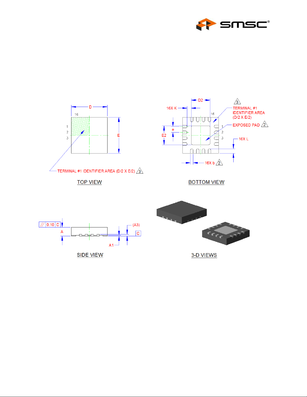
Multiple RPM-Based PWM Fan Controller for Five Fans
Datasheet
Chapter 7 Package Drawing
7.1 EMC2305 Package Information
Figure 7.1 Package Drawing - 16-Pin Q FN 4mm x 4mm
SMSC EMC2305 53 Revision 1.3 (05-18-11)
DATASHEET
Page 54
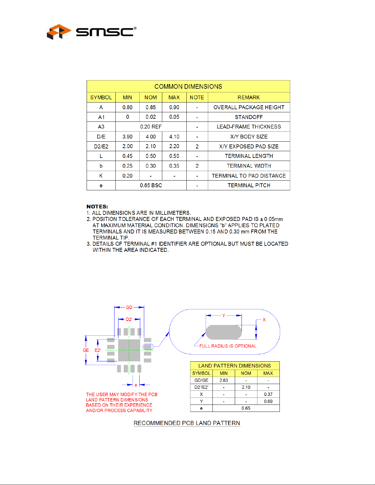
Multiple RPM-Based PWM Fan Controller for Five Fans
Datasheet
Figure 7.2 Package Dimensions - 16-Pin QFN 4mm x 4mm
Figure 7.3 PCB Footprint - 16-Pin QFN 4mm x 4mm
Revision 1.3 (05-18-11) 54 SMSC EMC2305
DATASHEET
Page 55
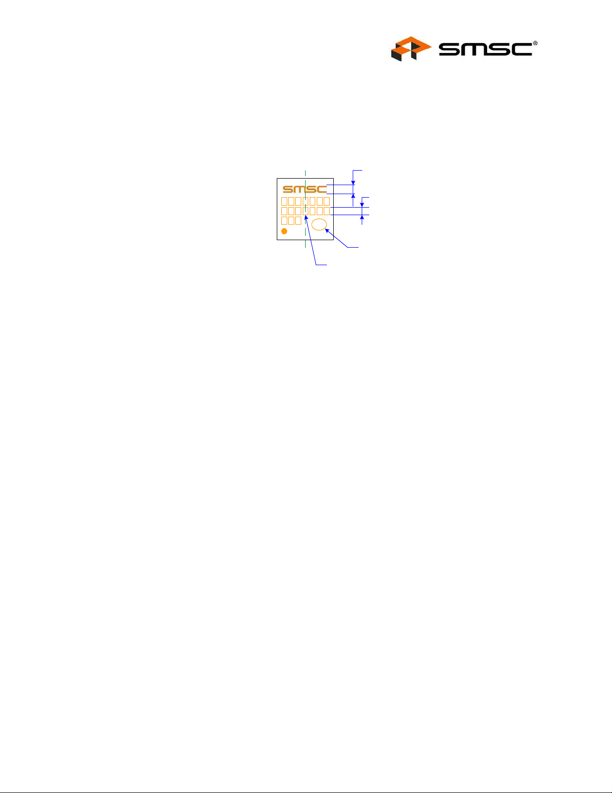
Multiple RPM-Based PWM Fan Controller for Five Fans
BOTTOM
BOTTOM MARKING NOT ALLOW ED
LINE: 1 – SMSC Logo without circled (R) symbol
LINE: 2 – Device Number
LINE: 3 – Last 7 digits of Lot Number
LINE: 4 – Revision and Country Code (RCC)
LINES 1 to 3: CENTER HORIZONTAL ALIGNMENT
LINE 4: LEFT HORIZONTAL ALIGNMENT
PB-FREE/GREEN SYMBOL
(Matte Sn )
0.41
3x 0.56
TOP
e3
PIN 1
2305
CCR
123456a
-
1
Datasheet
7.2 Package Markings
Figure 7.4 EMC2305 Package Markings
SMSC EMC2305 55 Revision 1.3 (05-18-11)
DATASHEET
Page 56

Multiple RPM-Based PWM Fan Controller for Five Fans
Chapter 8 Datasheet Revision History
T able 8.1 Customer Revision History
REVISION LEVEL & DATE SECTION/FIGURE/ENTRY CORRECTION
Datasheet
Rev. 1.3 (05-18-11)
Rev. 1.2 (03-22-10) Table 2.3, "SMBus Electrical
Rev. 1.1 (10-12-09) Table 2.2, "Electrical
Rev. 1.0 (05-15-09) Initial release of datasheet
Section 4.8, "Watchdog
Timer"
Section 5.2, "Configuration
Register"
Specifications"
Specifications"
Chapter 6, Typical
Operating Curves
The ALERT# pin is asserted when the watchdog is
triggered.
Corrected description for MASK bit. Changed “If
any bit in either status register is set, the ALERT#
pins will be asserted (unless individually masked
via the Mask Register)” to “If any bit in the status
registers is set, the ALERT# pin will be asserted
(unless individually masked via the Fan Interrupt
Enable Register)”.
Updated SMBus Data Hold Time spec to 0 us
Tachometer Settin g Accuracy max was changed
from +/-3% to +/-2%.
Added typical operating curves
Revision 1.3 (05-18-11) 56 SMSC EMC2305
DATASHEET
Page 57

 Loading...