

Page 1
ESMT/EMP
EMD2050
PWM Step-Up DC/DC Converter for Panel Backlight
General Description
The EMD2050 designed with high efficiency step up
DC/DC converter for driving white LEDs. The device
can drive up 3 white LEDs from a single Li-Ion battery
or a DC power 2.5V to 5.5V. The EMD2050 uses
current mode and pulse-width modulated (PWM)
operation. It switches at 1.2MHz and allows using
small inductor and both of input/output capacitors.
An internal compensation can reduce external
component.
The EMD2050 include under-voltage lockout, current
limit, over voltage and thermal shutdown protection.
The EMD2050 is available in SOT-26 package.
Applications
Mobile Phone
Digital Still Cameras
Portable applications
MP3 Players
GPS Receivers
Features
WLEDs supports (20mA for each channel):
Up to 3S13P at VIN=3.7V
Up to 3S18P at VIN=5.0V
(Note: SÆ Series; PÆ Parallel)
Low Quiescent Current: 55 μA
Over Voltage Protection: 15V
Inherently Matched LED Current
Shutdown Current < 1μA
Reference Voltage 0.235V
Efficiency : 85% (Typ) at VIN=5.0V
PWM Dimming Control
Internal Soft Start and Compensation
Low Profile SOT-26 Package
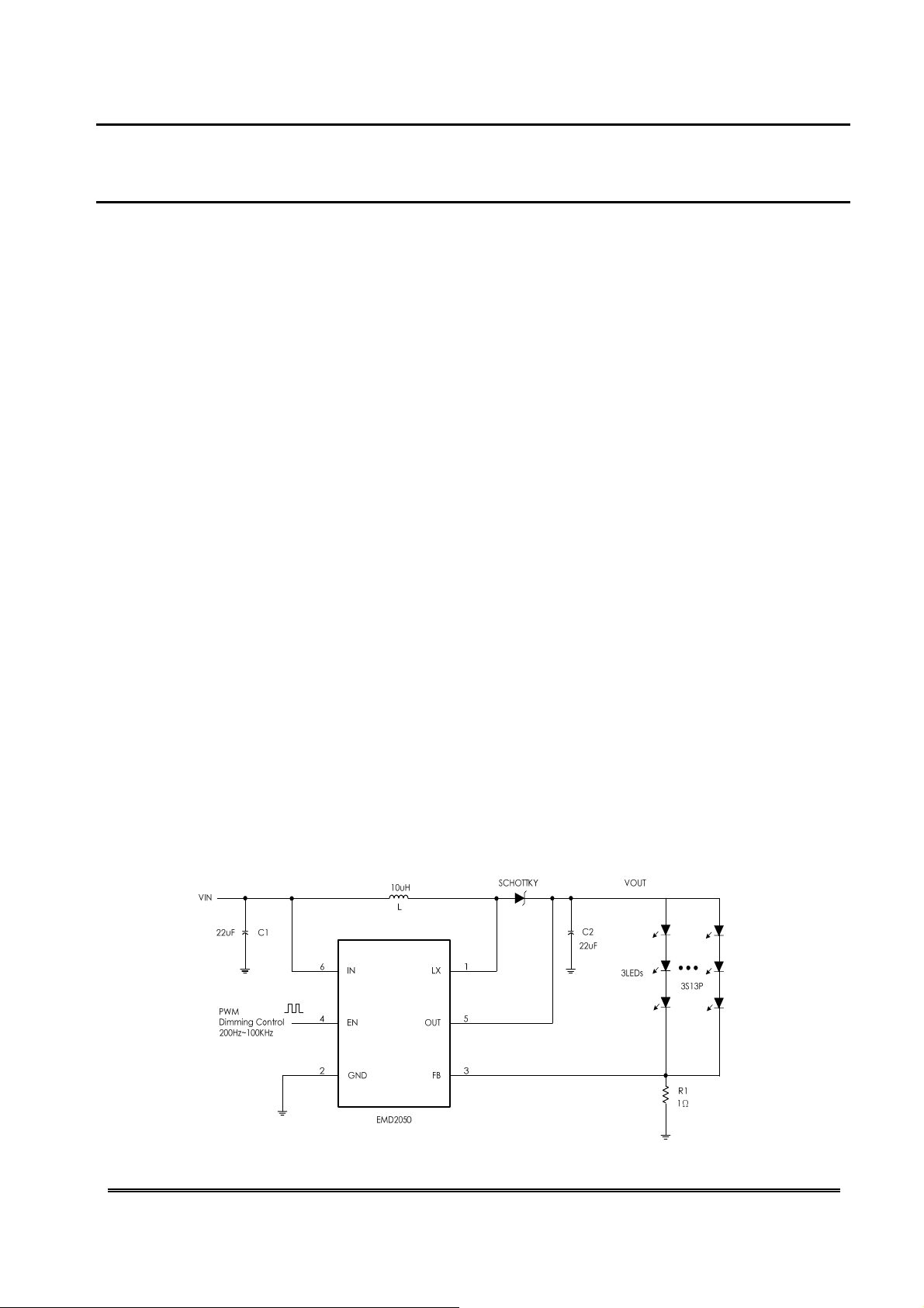
Typical Application (3S13P)
Fig.1
Elite Semiconductor Memory Technology Inc. /Elite MicroPower Inc. Publication Date: Oct. 2009
Revision: 1.0 1/12
Page 2

ESMT/EMP
EMD2050
Connection Diagram
Order Information
IN
LX GND FB
OUT
65 4
1 32
55
SOT-26
EN
EMD2050-00VC06NRR
00 Output voltage
VC06 SOT-26 Package
NRR RoHS & Halogen free package
Rating: -40 to 85°C
GRR RoHS Package (By Request)
Package in Tape & Reel
Order, Mark & Packing Information
Package Vout Product ID Marking Packing
OUT
SOT-26 Adjustable EMD2050-00VC06NRR
PIN1 DOT
IN
65 4
Tracking Code
1 32
LX GND FB
55
2050
EN
Tape & Reel
3Kpcs
Pin Functions
Pin Name
LX 1
GND 2 Ground Pin.
FB 3
EN 4
OUT 5 Over Voltage Protection Pin.
IN 6 Input Voltage Pin.
SOT-26
Pin #
Switch Pin.
Connect inductor/diode here.
Feedback Pin.
Reference voltage is 0.235V, connect cathode of lowest LED
and resistor here.
Chip Enable Pin.
Connect to 1.2V or higher to enable device, 0.4V or less to
disable device.
Function
Elite Semiconductor Memory Technology Inc. /Elite MicroPower Inc. Publication Date: Oct. 2009
Revision: 1.0 2/12
Page 3

ESMT/EMP
EMD2050
Absolute Maximum Ratings
Devices are subjected to failure if they stay above absolute maximum ratings
Input Voltage – 0.3V to 6V
EN, VFB Voltages – 0.3V to VIN
LX ,OUT Voltage – 0.3V to 16V
ESD Susceptibility HBM 2kV
MM 200V
Operating Temperature Range –40°C to 85°C
Storage Temperature –65°C to 150°C
Junction Temperature 150°C
Lead Temperature (Soldering, 10 sec) 260°C
Electrical Characteristics
(VCC = 3.7V, TA = 25°C, unless otherwise specified.)
PARAMETER TEST CONDITION MIN TYP MAX UNIT
Under Voltage Lock Out 1.8 2.4 V
Supply Current Continuously Switching 1 mA
Quiescent Current No Switching, VFB = 1V
Shutdown Current VEN < 0.4V 1 uA
Operation Frequency 0.9 1.2 1.5 MHz
Maximum Duty Cycle 93 95 %
Feedback Voltage 0.2115 0.235 0.2585 V
Thermal Shutdown Protection 160
Thermal Shutdown Hysteresis 20
Ron Isw = 200mA 0.5 0.8 ohm
Current Limit 1.4 A
Shutdown Voltage Low 0.4 V
Enable Voltage High 1.2 V
EN Leakage Current 1.3 μA
OVP 15 V
OVP Hysteresis 0.2 1 3 V
47 55 70 μA
℃
℃
Elite Semiconductor Memory Technology Inc. /Elite MicroPower Inc. Publication Date: Oct. 2009
Revision: 1.0 3/12
Page 4
ESMT/EMP
EMD2050
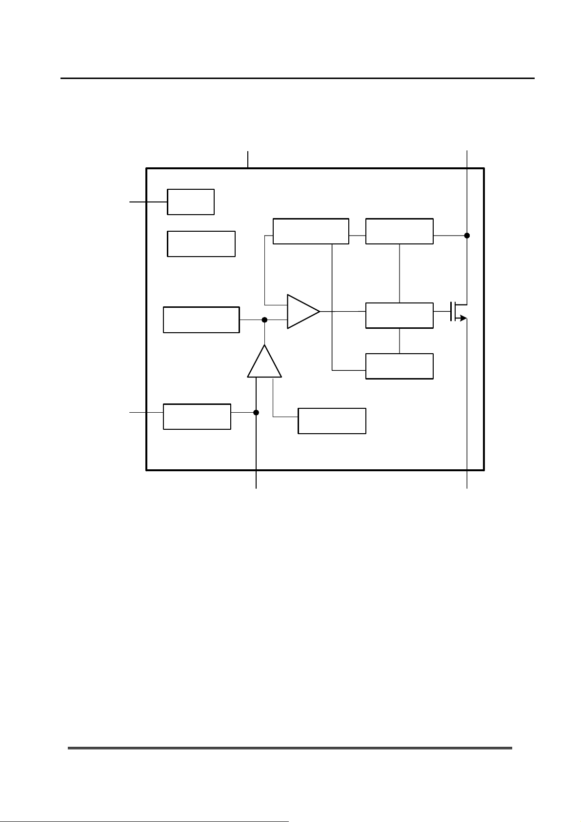
Function block
EN
OUT
EN
UVLO / OTP
INTERNAL
COMPENSATION
OVP
IN
_
+
SLOPE
COMPENSATION
_
+
VERF
LX
CURRENT
SENSER
LOGIC
BUFFER
OSC
GNDFB
Fig.2
Elite Semiconductor Memory Technology Inc. /Elite MicroPower Inc. Publication Date: Oct. 2009
Revision: 1.0 4/12
Page 5
ESMT/EMP
EMD2050
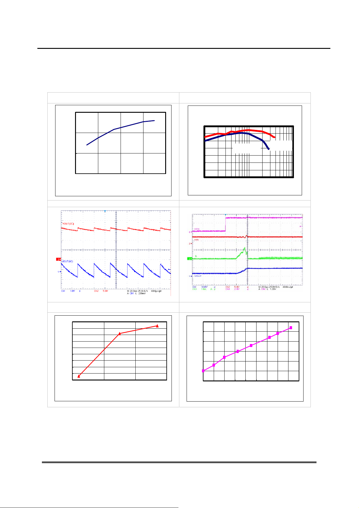
Typical Performance Characteristics
VIN=3.7V, unless otherwise specified
VIN vs. Efficiency (3S13P)
100
80
60
Efficiency (%)
40
23456
VIN ( V)
OVP Waveform Start-up Waveform
Load vs. Efficiency
EMD2050 Efficiency vs. Iout (Vout=9.5V, L=10uH
95
90
85
80
75
Efficiency (%)
70
65
60
10 100 1000
,Cin=Cout=10uF)
VIN=3.7V
Iout (mA)
VIN=5.0V
Fosc vs. Temperature Vfb vs. Temperature
1.22
1.21
1.20
1.19
1.18
1.17
1.16
Frequency (Hz)
1.15
1.14
1.13
-50 0 50 100
Temperature(℃)
0.255
0.25
0.245
0.24
VFB(V)
0.235
0.23
0.225
-40-200 20406080100120140
Temperature(℃)
Elite Semiconductor Memory Technology Inc. /Elite MicroPower Inc. Publication Date: Oct. 2009
Revision: 1.0 5/12
Page 6
ESMT/EMP
EMD2050
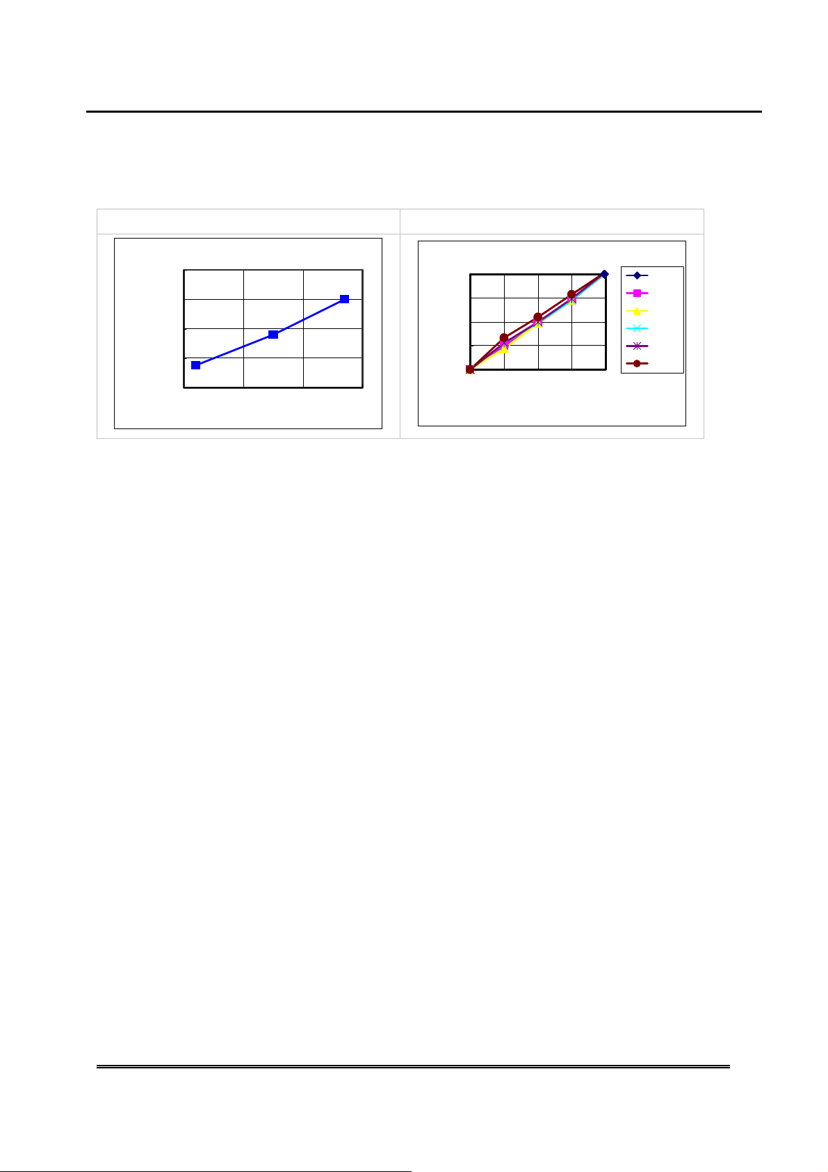
Typical Performance Characteristics
VIN=3.7V, unless otherwise specified
0.7500Ω
0.6500Ω
0.5500Ω
Rds
0.4500Ω
0.3500Ω
Rds vs. Temperature
Temperature vs Rds
-50
℃
0
℃
Temperature
20
15
10
ILEDs (mA)
5
0
50
℃
100
℃
PWM Duty vs. ILEDs
Duty vs ILEDs
200Hz
500Hz
1k
2k
32k
100k
0% 25% 50% 75% 100%
Duty (%)
Elite Semiconductor Memory Technology Inc. /Elite MicroPower Inc. Publication Date: Oct. 2009
Revision: 1.0 6/12
Page 7

ESMT/EMP
EMD2050
Application Information
Detailed Description
The EMD2050 is a constant frequency current-mode boost converter which can driver WLEDs 3S1P ~ 3S18P. The
device provides the same output current through each WLED that get even illumination. The fast operation
frequency allows for small inductor and input/output capacitors.
During normal operation, the internal oscillators send a pulse signal to set latch and turn on internal MOSFET
each duty circle. A current sense voltage sums MOSFET current and slope signal connected to the negative
terminal of the PWM comparator. When this signal voltage exceeds output voltage of error amplifier, the PWM
comparator will send a signal to reset latch and turn off internal MOSFET. The output voltage of error amplifier is
magnified from the difference between reference voltage and feedback voltage. If reference voltage is
higher than feedback voltage, more current is delivered to the output, the other way, less current is delivered.
UVLO
The EMD2050 provides under voltage lock out protection. When VIN is down close to UVLO threshold, the UVLO
block will send a signal to turn off power MOSFET. The device stops to supply current to output. The 100mV
hysteresis prevents supply transients from causing a restart. Once the VIN exceed UVLO threshold, the device
unlocks latch and turn power MOSFET.
Enable / Disable
The EMD2050 enter shutdown mode when EN pin voltage is less 0.4V. When in shutdown mode, all internal
circuits of the EMD2050 are turn off and quiescent current is reduced to 1uA. When driver EN pin voltage is
higher than 1.2V, start-up begins.
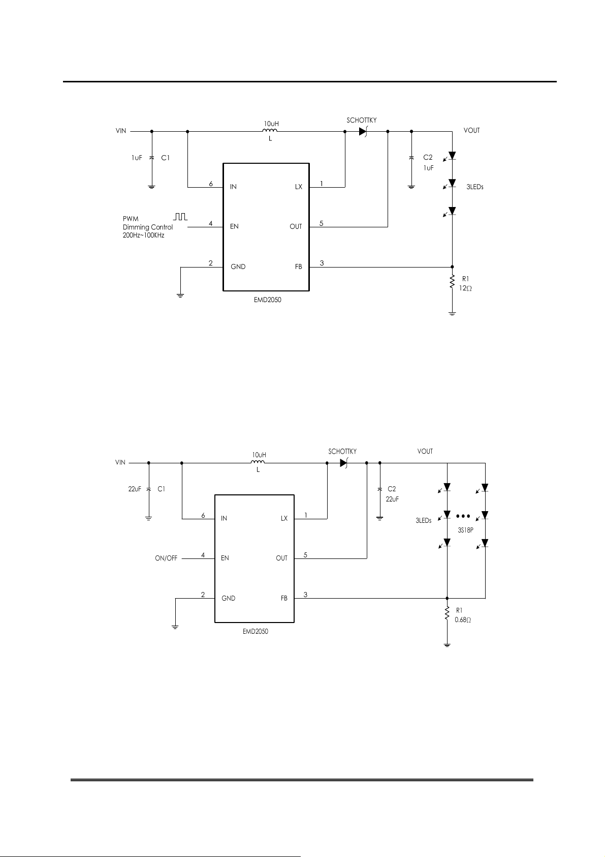
EN pin can be used for dimming control, the PWM frequency range is from 100Hz to 100kHz. The average LED
current is proportional to the PWM duty cycle, while 0% duty cycle triggers zero WLEDs current and 100% duty
cycle triggers full WLEDs current.
OVP
When WLEDs are open, the boost control loop just like open loop operation, it may causes over voltage
damage on LX pin. In order to prevent this damage, the EMD2050 provides OVP function to provide it. The
protection threshold is set at 15V.
OTP
The internal thermal sensor turn off power MOSFET when junction temperature is exceeded 160℃, the OTP is
designed with a 20℃ hysteresis.
Elite Semiconductor Memory Technology Inc. /Elite MicroPower Inc. Publication Date: Oct. 2009
Revision: 1.0 7/12
Page 8
ESMT/EMP
EMD2050
LED Current Setting
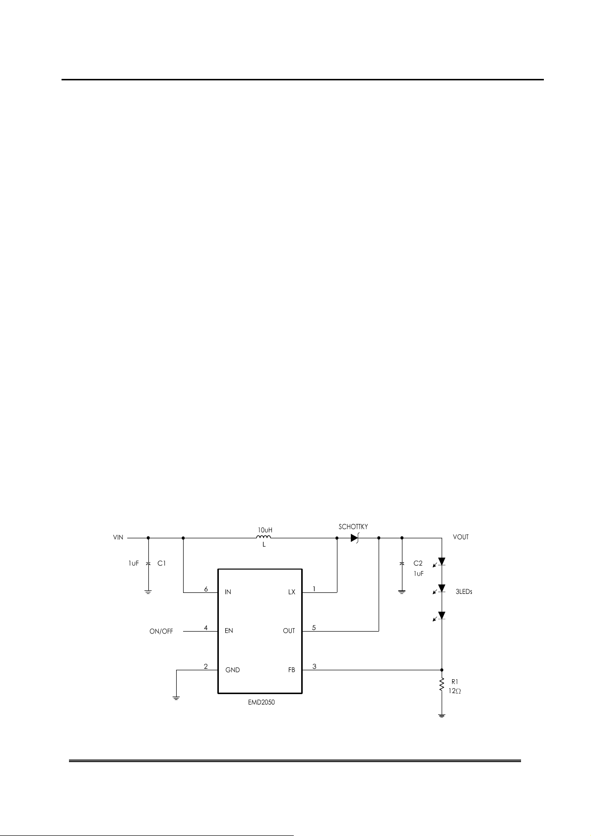
Referring to Figure 1 of the typical application, adjusting the output current changes the brightness of WLEDs,
the EMD2050 regulates output current by sense resistor (R1). The output current is given by:
LED current = 0.235V / R1
Cin and Cout Selection
It is recommended to use the X5R or X7R which have best temperature and voltage characteristics of all the
ceramics for a give value and size. A minimum input capacitance of 1μF is required for the EMD2050, The
capacitor value may be increased without limit. The typical output capacitor value is 1μF, Higher capacitance
can be used to reduce voltage ripple.
Inductor Selection
The inductor values range from 4.7μH to 22μH. The typical inductor value is 10μH. The low DCR inductor is
preferred. In addition, the limit saturation current of inductor must exceed current limit of the EMD2050.
Diode Selection
Referring to Figure 1 of the typical application, the EMD2050 is high switching control devise which demands a
high speed rectification diode for optimum efficiency. The schottky diode is preferred, for high efficiency,
schottky diode provide fast recovery time and low forward voltage that reduce power loss. The recover
breakdown voltage of schottky diode must exceed output voltage.
Application Circuit
Application circuit for 3S1P
z
Fig.3
Elite Semiconductor Memory Technology Inc. /Elite MicroPower Inc. Publication Date: Oct. 2009
Revision: 1.0 8/12
Page 9
ESMT/EMP
z Application circuit for 3S1P with dimming control
EMD2050
Fig.4
z
Application circuit for 3S18P (for VIN=5.0V application)
Fig.5
Elite Semiconductor Memory Technology Inc. /Elite MicroPower Inc. Publication Date: Oct. 2009
Revision: 1.0 9/12
Page 10
ESMT/EMP
EMD2050
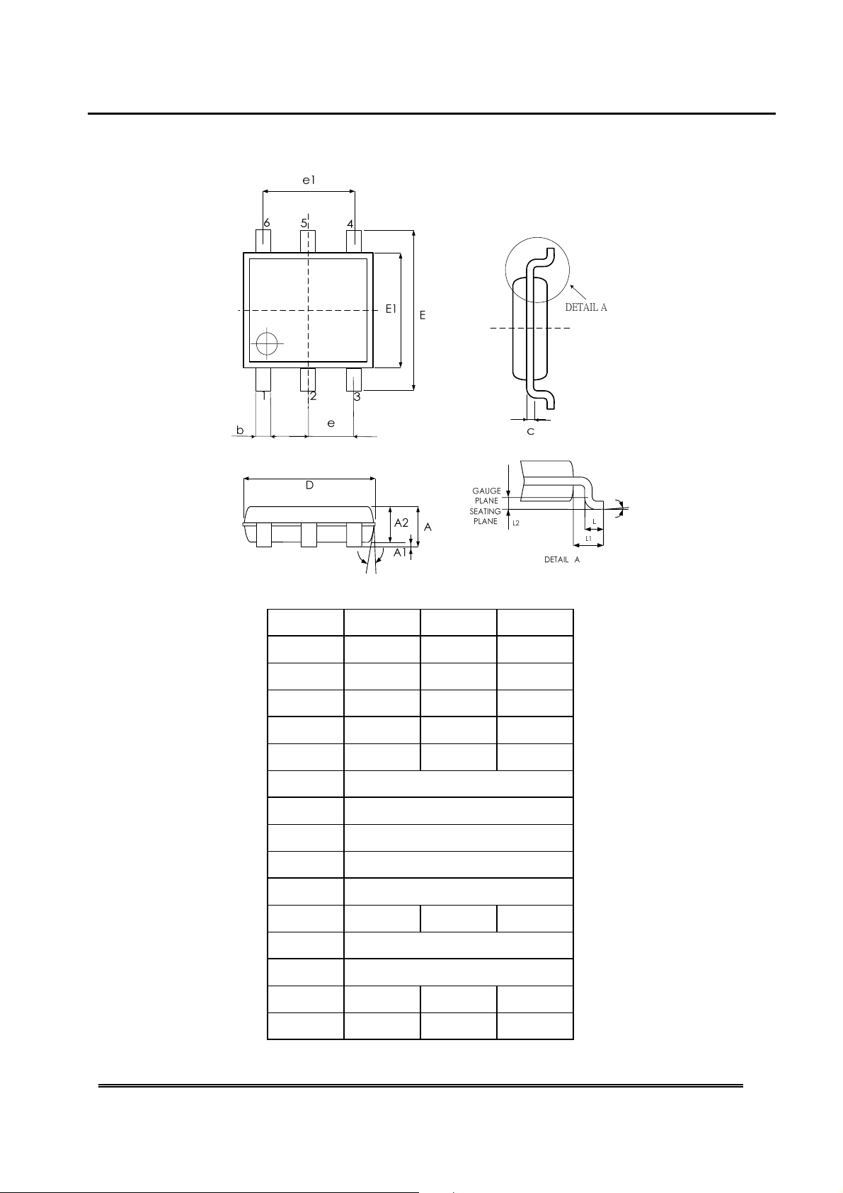
Package Outline
SOT-26
θ2
SYMBPLS MIN. NOM. MAX.
A
A1
A2 0.90 1.15
b 0.30
c 0.08
- -
- -
-
-
1.45
0.15
1.30
0.50
0.22
D 2.90 BSC.
E 2.80 BSC.
E1 1.60 BSC.
e 0.95 BSC
e1 1.90 BSC
L 0.30 0.45
0.60
o
θ
L1 0.60 REF
L2 0.25 REF
θ° 0 4 8
θ2° 5 10 15
Elite Semiconductor Memory Technology Inc. /Elite MicroPower Inc. Publication Date: Oct. 2009
Revision: 1.0 10/12
Page 11

ESMT/EMP
EMD2050
Revision History
Revision Date Description
0.1 2009.05.08 Original
1.0 2009.10.30 Removed the letters of “Preliminary”
Elite Semiconductor Memory Technology Inc. /Elite MicroPower Inc. Publication Date: Oct. 2009
Revision: 1.0 11/12
Page 12

ESMT/EMP
EMD2050
Important Notice
All rights reserved.
No part of this document may be reproduced or duplicated in any form or
by any means without the prior permission of ESMT.
The contents contained in this document are believed to be accurate at
the time of publication. ESMT assumes no responsibility for any error in this
document, and reserves the right to change the products or specification
in this document without notice.
The information contained herein is presented only as a guide or examples
for the application of our products. No responsibility is assumed by ESMT for
any infringement of patents, copyrights, or other intellectual property rights
of third parties which may result from its use. No license, either express ,
implied or otherwise, is granted under any patents, copyrights or other
intellectual property rights of ESMT or others.
Any semiconductor devices may have inherently a certain rate of failure.
To minimize risks associated with customer's application, adequate design
and operating safeguards against injury, damage, or loss from such failure,
should be provided by the customer when making application designs.
ESMT's products are not authorized for use in critical applications such as,
but not limited to, life support devices or system, where failure or abnormal
operation may directly affect human lives or cause physical injury or
property damage. If products described here are to be used for such kinds
of application, purchaser must do its own quality assurance testing
appropriate to such applications.
Elite Semiconductor Memory Technology Inc. /Elite MicroPower Inc. Publication Date: Oct. 2009
Revision: 1.0 12/12
Page 13

 Loading...