

Page 1

EMC2103
RPM-Based Fan
Controller with HW
Thermal Shutdown
PRODUCT FEATURES
The EMC2103 is an SMBus compliant fan controller with
up to up to 3 external and 1 internal temperature
channels. The fan driver can be operated using two
methods each with two modes. The methods include an
RPM based Fan Speed Control Algorithm and a direct
PWM drive setting. The modes include manually
programming the desired settings or using the internal
programmable temperature look-up table to select the
desired setting based on measured temperature.
The temperature monitors offer 1°C accuracy (for
external diodes) with sophisticated features to reduce
errors introduced by series resistance and beta variation
of substrate thermal diode transistors commonly found
in processors.
The EMC2103 also includes a hardware programmable
temperature limit and dedicated system shutdown
output for thermal protection of critical circuitry.
Applications
No tebook Computers
Projectors
Graphics Cards
Indu strial and Networking Equipment
Datasheet
Features
Programmable Fan Control circuit
— 4-wire fan compatible
— High and low frequency PWM
R PM based fan control algorithm
— 2.5% accuracy from 500RPM to 16k RPM
— Detects fan aging and variation
Temperature Look-Up Table
— Allows programmed fan response to temperature
— Controls fan speed or PWM drive setting
— Allows externally set temperature data to drive fan
— Supports DTS data from CPU
Up to Three External Temperature Channels
(EMC2103-2 only)
— Supports 45nm, 60nm, and 90nm CPU diodes
— Automatically detects and supports CPUs requiring BJT
or Transistor models
— Resistance error correction
— Supports discrete transistors (i.e. 2N3904)
— 1°C accurate (60°C to 125°C)
— 0.125°C resolution
H ardware Programmable Thermal Shutdown
Temperature
— Cannot be altered by software
— 65°C to 127°C Range
Prog rammable High and Low Limits for all channels
Interna l Temperature Monitor
— 2°C accuracy
— 0.125°C resolution
3 .3V Supply Voltage
SMBus 2.0 Compliant
— SMBus Alert compatible
Two dedicated GPIOs (EMC2103-2 and EMC2103-4
only)
Available in 12-pin, QFN Lead-Free RoHS Complia nt
Package (EMC2103-1 and EMC2103-3) or 16-pin,
QFN Lead-Free RoHS Compliant Package
(EMC2103-2 and EMC2103-4)
SMSC EMC2103 DATASHEET Revision 0.85 (01-29-08)
Page 2

RPM-Based Fan Controller with HW Thermal Shutdown
ORDER NUMBERS:
ORDERING NUMBER PACKAGE FEATURES
Datasheet
EMC2103-1-KP 12 pin, QFN Lead-Free, ROHS
Compliant
EMC2103-2-AP 16 pin, QFN Lead-Free, ROHS
Compliant
EMC2103-3-KP 12 pin, QFN Lead-Free, ROHS
Compliant
EMC2103-4-AP 16 pin, QFN Lead-Free, ROHS
Compliant
One external diode, RPM based
Fan Speed Control Algorithm, High
Frequency PWM driver, HW
Thermal / Critical shutdown,
EEPROM Load disabled
Up to three external diodes, RPM
based Fan Speed Control algorithm,
High Frequency PWM driver, HW
Thermal / Critical shutdown, 2
GPIOs, EEPROM Load disabled
One external diode, RPM based
Fan Speed Control Algorithm, High
Frequency PWM driver, HW
Thermal / Critical shutdown,
EEPROM Load enabled
Up to three external diodes, RPM
based Fan Speed Control algorithm,
High Frequency PWM driver, HW
Thermal / Critical shutdown, 2
GPIOs, EEPROM Load enabled
80 ARKAY DRIVE, HAUPPAUGE, NY 11788 (631) 435-6000, FAX (631) 273-3123
Copyright © 2008 SMSC or its subsidiaries. All rights reserved.
Circuit diagrams and other information relating to SMSC products are included as a mean s of illustrating typical applications. Conse quently, complete information sufficient for
construction purposes is not necessarily given. Although the information has been checked and is believed to be accurate, no responsibility is assumed for inaccuracies. SMSC
reserves the right to make changes to specifications and product descriptions at any time without notice. Contact your local SMSC sales office to obtain the latest specifications
before placing your product order. The provision of this information does not convey to the purchaser of the described semiconductor devices any licenses under any patent
rights or other intellectual property rights of SMSC or others. All sales are expressly conditional on your agreement to the terms and conditions of the most recently da ted
version of SMSC's standard Terms of Sale Agreement dated before the date of your order (the "Terms of Sale Agreement"). The product may contain design defects or errors
known as anomalies which may cause the product's functions to deviate from published specifications. Anomaly sheets are available upon request. SMSC products are not
designed, intended, authorized or warranted for use in any life support or other application where product failure could cause or contribute to personal injury or severe property
damage. Any and all such uses without prior written approval of an Officer of SMSC and further testing and/or modification will be fully at the risk of the customer. Copies of
this document or other SMSC literature, as well as the Terms of Sale Agreement, may be obtained by visiting SMSC’s website at http://www.smsc.com. SMSC is a registered
trademark of Standard Microsystems Corporation (“SMSC”). Product names and company names are the trademarks of their respective holders.
SMSC DISCLAIMS AND EXCLUDES ANY AND ALL WARRANTIES, INCLUDING WITHOUT LIMITATION ANY AND ALL IMPLIED WARRANTIES OF MERCHANTABILITY,
FITNESS FOR A PARTICULAR PURPOSE, TITLE, AND AGAINST INFRINGEMENT AND THE LIKE, AND ANY AND ALL WARRANTIES ARISING FROM ANY COURSE
OF DEALING OR USAGE OF TRADE. IN NO EVENT SHALL SMSC BE LIABLE FOR ANY DIRECT, INCIDENTAL, INDIRECT, SPECIAL, PUNITIVE, OR CONSEQUENTIAL
DAMAGES; OR FOR LOST DATA, PROFITS, SAVINGS OR REVENUES OF ANY KIND; REGARDLESS OF THE FORM OF ACTION, WHETHER BASED ON CONTRACT;
TORT; NEGLIGENCE OF SMSC OR OTHERS; STRICT LIABILITY; BREACH OF WARRANTY; OR OTHERWISE; WHETHER OR NOT ANY REMEDY OF BUYER IS HELD
TO HAVE FAILED OF ITS ESSENTIAL PURPOSE, AND WHETHER OR NOT SMSC HAS BEEN ADVISED OF THE POSSIBILITY OF SUCH DAMAGES.
Revision 0.85 (01-29-08) 2 SMSC EMC2103
DATASHEET
Page 3

RPM-Based Fan Controller with HW Thermal Shutdown
Datasheet
Table of Contents
Chapter 1 Block Diagram . . . . . . . . . . . . . . . . . . . . . . . . . . . . . . . . . . . . . . . . . . . . . . . . . . . . . 8
Chapter 2 Pin Layout . . . . . . . . . . . . . . . . . . . . . . . . . . . . . . . . . . . . . . . . . . . . . . . . . . . . . . . . 9
Chapter 3 Electrical Characteristics . . . . . . . . . . . . . . . . . . . . . . . . . . . . . . . . . . . . . . . . . . . 13
3.1 Electrical Specifications . . . . . . . . . . . . . . . . . . . . . . . . . . . . . . . . . . . . . . . . . . . . . . . . . . . . . . . . . 14
3.2 SMBus Electrical Specifications (Client Mode). . . . . . . . . . . . . . . . . . . . . . . . . . . . . . . . . . . . . . . . 15
Chapter 4 Communications . . . . . . . . . . . . . . . . . . . . . . . . . . . . . . . . . . . . . . . . . . . . . . . . . . 17
4.1 System Management Bus Interface Protocol . . . . . . . . . . . . . . . . . . . . . . . . . . . . . . . . . . . . . . . . . 17
4.2 Write Byte . . . . . . . . . . . . . . . . . . . . . . . . . . . . . . . . . . . . . . . . . . . . . . . . . . . . . . . . . . . . . . . . . . . . 17
4.3 Read Byte. . . . . . . . . . . . . . . . . . . . . . . . . . . . . . . . . . . . . . . . . . . . . . . . . . . . . . . . . . . . . . . . . . . . 18
4.4 Send Byte. . . . . . . . . . . . . . . . . . . . . . . . . . . . . . . . . . . . . . . . . . . . . . . . . . . . . . . . . . . . . . . . . . . . 18
4.5 Receive Byte. . . . . . . . . . . . . . . . . . . . . . . . . . . . . . . . . . . . . . . . . . . . . . . . . . . . . . . . . . . . . . . . . . 18
4.6 Alert Response Address. . . . . . . . . . . . . . . . . . . . . . . . . . . . . . . . . . . . . . . . . . . . . . . . . . . . . . . . . 18
4.7 SMBus Address . . . . . . . . . . . . . . . . . . . . . . . . . . . . . . . . . . . . . . . . . . . . . . . . . . . . . . . . . . . . . . . 19
4.8 SMBus Time-out. . . . . . . . . . . . . . . . . . . . . . . . . . . . . . . . . . . . . . . . . . . . . . . . . . . . . . . . . . . . . . . 19
Chapter 5 General Description. . . . . . . . . . . . . . . . . . . . . . . . . . . . . . . . . . . . . . . . . . . . . . . . 20
5.1 Critical/Thermal Shutdown . . . . . . . . . . . . . . . . . . . . . . . . . . . . . . . . . . . . . . . . . . . . . . . . . . . . . . . 21
5.1.1 SHDN_SEL Pin . . . . . . . . . . . . . . . . . . . . . . . . . . . . . . . . . . . . . . . . . . . . . . . . . . . . . . . . 22
5.1.2 TRIP_SET Pin . . . . . . . . . . . . . . . . . . . . . . . . . . . . . . . . . . . . . . . . . . . . . . . . . . . . . . . . . 22
5.2 Fan Control Modes of Operation . . . . . . . . . . . . . . . . . . . . . . . . . . . . . . . . . . . . . . . . . . . . . . . . . . 24
5.3 PWM Fan Driver . . . . . . . . . . . . . . . . . . . . . . . . . . . . . . . . . . . . . . . . . . . . . . . . . . . . . . . . . . . . . . . 25
5.4 Fan Control Look-Up Table . . . . . . . . . . . . . . . . . . . . . . . . . . . . . . . . . . . . . . . . . . . . . . . . . . . . . . 25
5.4.1 Programming the Look Up Table. . . . . . . . . . . . . . . . . . . . . . . . . . . . . . . . . . . . . . . . . . . 26
5.4.2 DTS Support . . . . . . . . . . . . . . . . . . . . . . . . . . . . . . . . . . . . . . . . . . . . . . . . . . . . . . . . . . 27
5.5 RPM based Fan Speed Control Algorithm (FSC). . . . . . . . . . . . . . . . . . . . . . . . . . . . . . . . . . . . . . 27
5.5.1 Programming the RPM Based Fan Speed Control Algorithm . . . . . . . . . . . . . . . . . . . . . 28
5.6 Tachometer Measurement . . . . . . . . . . . . . . . . . . . . . . . . . . . . . . . . . . . . . . . . . . . . . . . . . . . . . . . 29
5.6.1 Stalled Fan . . . . . . . . . . . . . . . . . . . . . . . . . . . . . . . . . . . . . . . . . . . . . . . . . . . . . . . . . . . 29
5.6.2 Aging Fan or Invalid Drive Detection. . . . . . . . . . . . . . . . . . . . . . . . . . . . . . . . . . . . . . . . 29
5.7 Spin Up Routine . . . . . . . . . . . . . . . . . . . . . . . . . . . . . . . . . . . . . . . . . . . . . . . . . . . . . . . . . . . . . . . 30
5.8 Ramp Rate Control. . . . . . . . . . . . . . . . . . . . . . . . . . . . . . . . . . . . . . . . . . . . . . . . . . . . . . . . . . . . . 31
5.9 Watchdog Timer . . . . . . . . . . . . . . . . . . . . . . . . . . . . . . . . . . . . . . . . . . . . . . . . . . . . . . . . . . . . . . . 31
5.10 Fault Queue . . . . . . . . . . . . . . . . . . . . . . . . . . . . . . . . . . . . . . . . . . . . . . . . . . . . . . . . . . . . . . . . . . 32
5.11 Temperature Monitoring . . . . . . . . . . . . . . . . . . . . . . . . . . . . . . . . . . . . . . . . . . . . . . . . . . . . . . . . . 32
5.11.1 Dynamic Averaging . . . . . . . . . . . . . . . . . . . . . . . . . . . . . . . . . . . . . . . . . . . . . . . . . . . . . 32
5.11.2 Resistance Error Correction . . . . . . . . . . . . . . . . . . . . . . . . . . . . . . . . . . . . . . . . . . . . . . 32
5.11.3 Beta Compensation. . . . . . . . . . . . . . . . . . . . . . . . . . . . . . . . . . . . . . . . . . . . . . . . . . . . . 33
5.11.4 Digital Averaging . . . . . . . . . . . . . . . . . . . . . . . . . . . . . . . . . . . . . . . . . . . . . . . . . . . . . . . 33
5.12 Diode Connections . . . . . . . . . . . . . . . . . . . . . . . . . . . . . . . . . . . . . . . . . . . . . . . . . . . . . . . . . . . . . 33
5.12.1 Diode Faults . . . . . . . . . . . . . . . . . . . . . . . . . . . . . . . . . . . . . . . . . . . . . . . . . . . . . . . . . . 34
5.13 GPIOs. . . . . . . . . . . . . . . . . . . . . . . . . . . . . . . . . . . . . . . . . . . . . . . . . . . . . . . . . . . . . . . . . . . . . . . 34
Chapter 6 Register Set. . . . . . . . . . . . . . . . . . . . . . . . . . . . . . . . . . . . . . . . . . . . . . . . . . . . . . . 35
6.1 Register Map . . . . . . . . . . . . . . . . . . . . . . . . . . . . . . . . . . . . . . . . . . . . . . . . . . . . . . . . . . . . . . . . . 35
6.1.1 Lock Entries. . . . . . . . . . . . . . . . . . . . . . . . . . . . . . . . . . . . . . . . . . . . . . . . . . . . . . . . . . . 41
6.2 Temperature Data Registers . . . . . . . . . . . . . . . . . . . . . . . . . . . . . . . . . . . . . . . . . . . . . . . . . . . . . 42
6.3 Critical/Thermal Shutdown Temperature Register . . . . . . . . . . . . . . . . . . . . . . . . . . . . . . . . . . . . . 43
6.4 Pushed Temperature Registers . . . . . . . . . . . . . . . . . . . . . . . . . . . . . . . . . . . . . . . . . . . . . . . . . . . 43
SMSC EMC2103 3 Revision 0.85 (01-29-08)
DATASHEET
Page 4

RPM-Based Fan Controller with HW Thermal Shutdown
Datasheet
6.5 TRIP_SET Voltage Register. . . . . . . . . . . . . . . . . . . . . . . . . . . . . . . . . . . . . . . . . . . . . . . . . . . . . . 44
6.6 Ideality Factor Registers. . . . . . . . . . . . . . . . . . . . . . . . . . . . . . . . . . . . . . . . . . . . . . . . . . . . . . . . . 44
6.7 Beta Configuration Register . . . . . . . . . . . . . . . . . . . . . . . . . . . . . . . . . . . . . . . . . . . . . . . . . . . . . . 45
6.8 REC Configuration Register . . . . . . . . . . . . . . . . . . . . . . . . . . . . . . . . . . . . . . . . . . . . . . . . . . . . . . 46
6.9 Critical Temperature Limit Registers . . . . . . . . . . . . . . . . . . . . . . . . . . . . . . . . . . . . . . . . . . . . . . . 47
6.10 Configuration Register . . . . . . . . . . . . . . . . . . . . . . . . . . . . . . . . . . . . . . . . . . . . . . . . . . . . . . . . . . 47
6.11 Configuration 2 Register. . . . . . . . . . . . . . . . . . . . . . . . . . . . . . . . . . . . . . . . . . . . . . . . . . . . . . . . . 48
6.12 Interrupt Status Register. . . . . . . . . . . . . . . . . . . . . . . . . . . . . . . . . . . . . . . . . . . . . . . . . . . . . . . . . 49
6.13 Error Status Registers . . . . . . . . . . . . . . . . . . . . . . . . . . . . . . . . . . . . . . . . . . . . . . . . . . . . . . . . . . 50
6.13.1 Tcrit Status Register . . . . . . . . . . . . . . . . . . . . . . . . . . . . . . . . . . . . . . . . . . . . . . . . . . . . 50
6.14 Fan Status Register . . . . . . . . . . . . . . . . . . . . . . . . . . . . . . . . . . . . . . . . . . . . . . . . . . . . . . . . . . . . 51
6.15 Interrupt Enable Register . . . . . . . . . . . . . . . . . . . . . . . . . . . . . . . . . . . . . . . . . . . . . . . . . . . . . . . . 51
6.16 Fan Interrupt Enable Register. . . . . . . . . . . . . . . . . . . . . . . . . . . . . . . . . . . . . . . . . . . . . . . . . . . . . 52
6.17 PWM Configuration Register . . . . . . . . . . . . . . . . . . . . . . . . . . . . . . . . . . . . . . . . . . . . . . . . . . . . . 52
6.18 PWM Base Frequency Register . . . . . . . . . . . . . . . . . . . . . . . . . . . . . . . . . . . . . . . . . . . . . . . . . . . 53
6.19 Limit Registers . . . . . . . . . . . . . . . . . . . . . . . . . . . . . . . . . . . . . . . . . . . . . . . . . . . . . . . . . . . . . . . . 53
6.20 Fan Setting Registers. . . . . . . . . . . . . . . . . . . . . . . . . . . . . . . . . . . . . . . . . . . . . . . . . . . . . . . . . . . 54
6.21 PWM Divide Register . . . . . . . . . . . . . . . . . . . . . . . . . . . . . . . . . . . . . . . . . . . . . . . . . . . . . . . . . . . 54
6.22 Fan Configuration 1 Register . . . . . . . . . . . . . . . . . . . . . . . . . . . . . . . . . . . . . . . . . . . . . . . . . . . . . 55
6.23 Fan Configuration 2 Register . . . . . . . . . . . . . . . . . . . . . . . . . . . . . . . . . . . . . . . . . . . . . . . . . . . . . 56
6.24 Gain Register . . . . . . . . . . . . . . . . . . . . . . . . . . . . . . . . . . . . . . . . . . . . . . . . . . . . . . . . . . . . . . . . . 58
6.25 Fan Spin Up Configuration Register. . . . . . . . . . . . . . . . . . . . . . . . . . . . . . . . . . . . . . . . . . . . . . . . 58
6.26 Fan Step Register. . . . . . . . . . . . . . . . . . . . . . . . . . . . . . . . . . . . . . . . . . . . . . . . . . . . . . . . . . . . . . 60
6.27 Fan Minimum Drive Register . . . . . . . . . . . . . . . . . . . . . . . . . . . . . . . . . . . . . . . . . . . . . . . . . . . . . 60
6.28 Valid TACH Count Register . . . . . . . . . . . . . . . . . . . . . . . . . . . . . . . . . . . . . . . . . . . . . . . . . . . . . . 61
6.29 Fan Drive Fail Band Registers . . . . . . . . . . . . . . . . . . . . . . . . . . . . . . . . . . . . . . . . . . . . . . . . . . . . 61
6.30 TACH Target Register . . . . . . . . . . . . . . . . . . . . . . . . . . . . . . . . . . . . . . . . . . . . . . . . . . . . . . . . . . 62
6.31 TACH Reading Register. . . . . . . . . . . . . . . . . . . . . . . . . . . . . . . . . . . . . . . . . . . . . . . . . . . . . . . . . 62
6.32 Look Up Table Configuration Register . . . . . . . . . . . . . . . . . . . . . . . . . . . . . . . . . . . . . . . . . . . . . . 63
6.33 Look Up Table Registers . . . . . . . . . . . . . . . . . . . . . . . . . . . . . . . . . . . . . . . . . . . . . . . . . . . . . . . . 64
6.34 GPIO Direction Register (EMC2103-2 Only) . . . . . . . . . . . . . . . . . . . . . . . . . . . . . . . . . . . . . . . . . 65
6.35 GPIO Output Configuration Register (EMC2103-2 Only) . . . . . . . . . . . . . . . . . . . . . . . . . . . . . . . . 66
6.36 GPIO Input Register (EMC2103-2 Only) . . . . . . . . . . . . . . . . . . . . . . . . . . . . . . . . . . . . . . . . . . . . 66
6.37 GPIO Output Register (EMC2103-2 Only) . . . . . . . . . . . . . . . . . . . . . . . . . . . . . . . . . . . . . . . . . . . 66
6.38 GPIO Interrupt Enable Register (EMC2103-2 Only). . . . . . . . . . . . . . . . . . . . . . . . . . . . . . . . . . . . 67
6.39 GPIO Status Register (EMC2103-2 Only) . . . . . . . . . . . . . . . . . . . . . . . . . . . . . . . . . . . . . . . . . . . 67
6.40 Software Lock Register. . . . . . . . . . . . . . . . . . . . . . . . . . . . . . . . . . . . . . . . . . . . . . . . . . . . . . . . . . 68
6.41 Product Features Register . . . . . . . . . . . . . . . . . . . . . . . . . . . . . . . . . . . . . . . . . . . . . . . . . . . . . . . 68
6.42 Product ID Register . . . . . . . . . . . . . . . . . . . . . . . . . . . . . . . . . . . . . . . . . . . . . . . . . . . . . . . . . . . . 69
6.43 Manufacturer ID Register . . . . . . . . . . . . . . . . . . . . . . . . . . . . . . . . . . . . . . . . . . . . . . . . . . . . . . . . 69
6.44 Revision Register . . . . . . . . . . . . . . . . . . . . . . . . . . . . . . . . . . . . . . . . . . . . . . . . . . . . . . . . . . . . . . 69
Chapter 7 Package Drawing . . . . . . . . . . . . . . . . . . . . . . . . . . . . . . . . . . . . . . . . . . . . . . . . . . 70
7.1 EMC2103-1 Package Information. . . . . . . . . . . . . . . . . . . . . . . . . . . . . . . . . . . . . . . . . . . . . . . . . . 70
7.2 EMC2103-2 Package Information. . . . . . . . . . . . . . . . . . . . . . . . . . . . . . . . . . . . . . . . . . . . . . . . . . 73
Appendix ALook Up Table Operation. . . . . . . . . . . . . . . . . . . . . . . . . . . . . . . . . . . . . . . . . . . 76
A.1 Example #1. . . . . . . . . . . . . . . . . . . . . . . . . . . . . . . . . . . . . . . . . . . . . . . . . . . . . . . . . . . . . . . . . . . 76
A.2 Example #2. . . . . . . . . . . . . . . . . . . . . . . . . . . . . . . . . . . . . . . . . . . . . . . . . . . . . . . . . . . . . . . . . . . 78
Appendix BRPM to Tachometer Count Look Up Tables . . . . . . . . . . . . . . . . . . . . . . . . . . . 80
B.1 1k RPM Range . . . . . . . . . . . . . . . . . . . . . . . . . . . . . . . . . . . . . . . . . . . . . . . . . . . . . . . . . . . . . . . . 80
Revision 0.85 (01-29-08) 4 SMSC EMC2103
DATASHEET
Page 5

RPM-Based Fan Controller with HW Thermal Shutdown
Datasheet
List of Figures
Figure 1.1 EMC2103 Block Diagram. . . . . . . . . . . . . . . . . . . . . . . . . . . . . . . . . . . . . . . . . . . . . . . . . . . . . 8
Figure 2.1 EMC2103-1 Pin Diagram (12 Pin QFN). . . . . . . . . . . . . . . . . . . . . . . . . . . . . . . . . . . . . . . . . . 9
Figure 2.2 EMC2103-2 Pin Diagram (16 pin QFN) . . . . . . . . . . . . . . . . . . . . . . . . . . . . . . . . . . . . . . . . 10
Figure 4.1 SMBus Timing Diagram. . . . . . . . . . . . . . . . . . . . . . . . . . . . . . . . . . . . . . . . . . . . . . . . . . . . . 17
Figure 5.1 System Diagram for EMC2103 . . . . . . . . . . . . . . . . . . . . . . . . . . . . . . . . . . . . . . . . . . . . . . . 20
Figure 5.2 Block Diagram of Critical / Thermal Shutdown. . . . . . . . . . . . . . . . . . . . . . . . . . . . . . . . . . . . 21
Figure 5.3 Fan Control Look-Up Table Example. . . . . . . . . . . . . . . . . . . . . . . . . . . . . . . . . . . . . . . . . . . 26
Figure 5.4 RPM based Fan Speed Control Algorithm. . . . . . . . . . . . . . . . . . . . . . . . . . . . . . . . . . . . . . . 28
Figure 5.5 Spin Up Routine. . . . . . . . . . . . . . . . . . . . . . . . . . . . . . . . . . . . . . . . . . . . . . . . . . . . . . . . . . . 30
Figure 5.6 Ramp Rate Control . . . . . . . . . . . . . . . . . . . . . . . . . . . . . . . . . . . . . . . . . . . . . . . . . . . . . . . . 31
Figure 5.7 Diode Connections. . . . . . . . . . . . . . . . . . . . . . . . . . . . . . . . . . . . . . . . . . . . . . . . . . . . . . . . . 33
Figure 7.1 Preliminary 12 pin QFN 4mm x 4mm Package Dimensions . . . . . . . . . . . . . . . . . . . . . . . . . 70
Figure 7.2 Preliminary 12 Pin QFN 4mm x 4mm Package Drawing . . . . . . . . . . . . . . . . . . . . . . . . . . . . 71
Figure 7.3 Recommended PCB Footprint 12-pin QFN 4mm x 4mm. . . . . . . . . . . . . . . . . . . . . . . . . . . . 72
Figure 7.4 Preliminary 16 Pin QFN 4mm x 4mm Package Dimensions . . . . . . . . . . . . . . . . . . . . . . . . . 73
Figure 7.5 Preliminary 16 Pin QFN 4mm x 4mm Package Drawing . . . . . . . . . . . . . . . . . . . . . . . . . . . . 74
Figure 7.6 Recommended PCB Footprint 16-pin QFN 4mm x 4mm. . . . . . . . . . . . . . . . . . . . . . . . . . . . 75
SMSC EMC2103 5 Revision 0.85 (01-29-08)
DATASHEET
Page 6

RPM-Based Fan Controller with HW Thermal Shutdown
Datasheet
List of Tables
Table 2.1 Pin Description for EMC2103 . . . . . . . . . . . . . . . . . . . . . . . . . . . . . . . . . . . . . . . . . . . . . . . . . 10
Table 2.2 Pin Types. . . . . . . . . . . . . . . . . . . . . . . . . . . . . . . . . . . . . . . . . . . . . . . . . . . . . . . . . . . . . . . . . 12
Table 3.1 Absolute Maximum Ratings. . . . . . . . . . . . . . . . . . . . . . . . . . . . . . . . . . . . . . . . . . . . . . . . . . . 13
Table 3.2 Electrical Specifications. . . . . . . . . . . . . . . . . . . . . . . . . . . . . . . . . . . . . . . . . . . . . . . . . . . . . . 14
Table 3.3 SMBus Electrical Specifications . . . . . . . . . . . . . . . . . . . . . . . . . . . . . . . . . . . . . . . . . . . . . . . 15
Table 4.1 Protocol Format . . . . . . . . . . . . . . . . . . . . . . . . . . . . . . . . . . . . . . . . . . . . . . . . . . . . . . . . . . . . 17
Table 4.2 Write Byte Protocol . . . . . . . . . . . . . . . . . . . . . . . . . . . . . . . . . . . . . . . . . . . . . . . . . . . . . . . . . 17
Table 4.3 Read Byte Protocol . . . . . . . . . . . . . . . . . . . . . . . . . . . . . . . . . . . . . . . . . . . . . . . . . . . . . . . . . 18
Table 4.4 Send Byte Protocol . . . . . . . . . . . . . . . . . . . . . . . . . . . . . . . . . . . . . . . . . . . . . . . . . . . . . . . . . 18
Table 4.5 Receive Byte Protocol . . . . . . . . . . . . . . . . . . . . . . . . . . . . . . . . . . . . . . . . . . . . . . . . . . . . . . . 18
Table 4.6 Alert Response Address Protocol . . . . . . . . . . . . . . . . . . . . . . . . . . . . . . . . . . . . . . . . . . . . . . 18
Table 5.1 SHDN_SEL Pin Decode . . . . . . . . . . . . . . . . . . . . . . . . . . . . . . . . . . . . . . . . . . . . . . . . . . . . . 22
Table 5.2 TRIP_SET Resistor Setting . . . . . . . . . . . . . . . . . . . . . . . . . . . . . . . . . . . . . . . . . . . . . . . . . . . 23
Table 5.3 Fan Controls Active for Operating Mode . . . . . . . . . . . . . . . . . . . . . . . . . . . . . . . . . . . . . . . . . 24
Table 5.4 Dynamic Averaging Behavior . . . . . . . . . . . . . . . . . . . . . . . . . . . . . . . . . . . . . . . . . . . . . . . . . 32
Table 6.1 EMC2103 Register Set . . . . . . . . . . . . . . . . . . . . . . . . . . . . . . . . . . . . . . . . . . . . . . . . . . . . . . 35
Table 6.2 Temperature Data Registers . . . . . . . . . . . . . . . . . . . . . . . . . . . . . . . . . . . . . . . . . . . . . . . . . . 42
Table 6.3 Temperature Data Format. . . . . . . . . . . . . . . . . . . . . . . . . . . . . . . . . . . . . . . . . . . . . . . . . . . . 42
Table 6.4 Critical/Thermal Shutdown Temperature Register. . . . . . . . . . . . . . . . . . . . . . . . . . . . . . . . . . 43
Table 6.5 Critical / Thermal Shutdown Data Format . . . . . . . . . . . . . . . . . . . . . . . . . . . . . . . . . . . . . . . . 43
Table 6.6 Pushed Temperature Register. . . . . . . . . . . . . . . . . . . . . . . . . . . . . . . . . . . . . . . . . . . . . . . . . 43
Table 6.7 TRIP_SET Voltage Register . . . . . . . . . . . . . . . . . . . . . . . . . . . . . . . . . . . . . . . . . . . . . . . . . . 44
Table 6.8 Ideality Factor Registers . . . . . . . . . . . . . . . . . . . . . . . . . . . . . . . . . . . . . . . . . . . . . . . . . . . . . 44
Table 6.9 Ideality Factor Look-Up Table . . . . . . . . . . . . . . . . . . . . . . . . . . . . . . . . . . . . . . . . . . . . . . . . . 44
Table 6.10 Beta Configuration Register. . . . . . . . . . . . . . . . . . . . . . . . . . . . . . . . . . . . . . . . . . . . . . . . . . . 45
Table 6.11 Beta Compensation Look Up Table. . . . . . . . . . . . . . . . . . . . . . . . . . . . . . . . . . . . . . . . . . . . . 46
Table 6.12 REC Configuration Register . . . . . . . . . . . . . . . . . . . . . . . . . . . . . . . . . . . . . . . . . . . . . . . . . . 46
Table 6.13 Limit Registers . . . . . . . . . . . . . . . . . . . . . . . . . . . . . . . . . . . . . . . . . . . . . . . . . . . . . . . . . . . . 47
Table 6.14 Configuration Register. . . . . . . . . . . . . . . . . . . . . . . . . . . . . . . . . . . . . . . . . . . . . . . . . . . . . . . 47
Table 6.15 Configuration 2 Register . . . . . . . . . . . . . . . . . . . . . . . . . . . . . . . . . . . . . . . . . . . . . . . . . . . . . 48
Table 6.16 Fault Queue. . . . . . . . . . . . . . . . . . . . . . . . . . . . . . . . . . . . . . . . . . . . . . . . . . . . . . . . . . . . . . . 49
Table 6.17 Conversion Rate . . . . . . . . . . . . . . . . . . . . . . . . . . . . . . . . . . . . . . . . . . . . . . . . . . . . . . . . . . . 49
Table 6.18 Interrupt Status Register . . . . . . . . . . . . . . . . . . . . . . . . . . . . . . . . . . . . . . . . . . . . . . . . . . . . . 49
Table 6.19 Error Status Register. . . . . . . . . . . . . . . . . . . . . . . . . . . . . . . . . . . . . . . . . . . . . . . . . . . . . . . . 50
Table 6.20 Fan Status Register. . . . . . . . . . . . . . . . . . . . . . . . . . . . . . . . . . . . . . . . . . . . . . . . . . . . . . . . . 51
Table 6.21 Interrupt Enable Register. . . . . . . . . . . . . . . . . . . . . . . . . . . . . . . . . . . . . . . . . . . . . . . . . . . . . 51
Table 6.22 Fan Interrupt Enable Register . . . . . . . . . . . . . . . . . . . . . . . . . . . . . . . . . . . . . . . . . . . . . . . . . 52
Table 6.23 PWM Configuration Register . . . . . . . . . . . . . . . . . . . . . . . . . . . . . . . . . . . . . . . . . . . . . . . . . . 52
Table 6.24 PWM Base Frequency Register . . . . . . . . . . . . . . . . . . . . . . . . . . . . . . . . . . . . . . . . . . . . . . . 53
Table 6.25PWM_BASEx[1:0] it Decode . . . . . . . . . . . . . . . . . . . . . . . . . . . . . . . . . . . . . . . . . . . . . . . . . . 53
Table 6.26 Limit Registers . . . . . . . . . . . . . . . . . . . . . . . . . . . . . . . . . . . . . . . . . . . . . . . . . . . . . . . . . . . . 53
Table 6.27 Fan Driver Setting Register . . . . . . . . . . . . . . . . . . . . . . . . . . . . . . . . . . . . . . . . . . . . . . . . . . . 54
Table 6.28 PWM Divide Register. . . . . . . . . . . . . . . . . . . . . . . . . . . . . . . . . . . . . . . . . . . . . . . . . . . . . . . . 54
Table 6.29 Fan Configuration 1 Register. . . . . . . . . . . . . . . . . . . . . . . . . . . . . . . . . . . . . . . . . . . . . . . . . . 55
Table 6.30 Range Decode. . . . . . . . . . . . . . . . . . . . . . . . . . . . . . . . . . . . . . . . . . . . . . . . . . . . . . . . . . . . . 55
Table 6.31 Minimum Edges for Fan Rotation . . . . . . . . . . . . . . . . . . . . . . . . . . . . . . . . . . . . . . . . . . . . . . 56
Table 6.32 Update Time . . . . . . . . . . . . . . . . . . . . . . . . . . . . . . . . . . . . . . . . . . . . . . . . . . . . . . . . . . . . . . 56
Table 6.33 Fan Configuration 2 Register. . . . . . . . . . . . . . . . . . . . . . . . . . . . . . . . . . . . . . . . . . . . . . . . . . 56
Table 6.34 Derivative Options . . . . . . . . . . . . . . . . . . . . . . . . . . . . . . . . . . . . . . . . . . . . . . . . . . . . . . . . . . 57
Table 6.35 Error Range Options . . . . . . . . . . . . . . . . . . . . . . . . . . . . . . . . . . . . . . . . . . . . . . . . . . . . . . . . 58
Table 6.36 Gain Register. . . . . . . . . . . . . . . . . . . . . . . . . . . . . . . . . . . . . . . . . . . . . . . . . . . . . . . . . . . . . . 58
Table 6.37 Gain Decode . . . . . . . . . . . . . . . . . . . . . . . . . . . . . . . . . . . . . . . . . . . . . . . . . . . . . . . . . . . . . . 58
Revision 0.85 (01-29-08) 6 SMSC EMC2103
DATASHEET
Page 7

RPM-Based Fan Controller with HW Thermal Shutdown
Datasheet
Table 6.38 Fan Spin Up Configuration Register . . . . . . . . . . . . . . . . . . . . . . . . . . . . . . . . . . . . . . . . . . . . 58
Table 6.39 DRIVE_FAIL_CNT[1:0] Bit Decode. . . . . . . . . . . . . . . . . . . . . . . . . . . . . . . . . . . . . . . . . . . . . 59
Table 6.40 Spin Level . . . . . . . . . . . . . . . . . . . . . . . . . . . . . . . . . . . . . . . . . . . . . . . . . . . . . . . . . . . . . . . . 59
Table 6.41 Spin Time. . . . . . . . . . . . . . . . . . . . . . . . . . . . . . . . . . . . . . . . . . . . . . . . . . . . . . . . . . . . . . . . . 60
Table 6.42 Fan Step Register . . . . . . . . . . . . . . . . . . . . . . . . . . . . . . . . . . . . . . . . . . . . . . . . . . . . . . . . . . 60
Table 6.43 Minimum Fan Drive Register. . . . . . . . . . . . . . . . . . . . . . . . . . . . . . . . . . . . . . . . . . . . . . . . . . 60
Table 6.44 Valid TACH Count Register. . . . . . . . . . . . . . . . . . . . . . . . . . . . . . . . . . . . . . . . . . . . . . . . . . . 61
Table 6.45 Fan Drive Fail Band Registers. . . . . . . . . . . . . . . . . . . . . . . . . . . . . . . . . . . . . . . . . . . . . . . . . 61
Table 6.46 TACH Target Register. . . . . . . . . . . . . . . . . . . . . . . . . . . . . . . . . . . . . . . . . . . . . . . . . . . . . . . 62
Table 6.47 TACH Reading Register . . . . . . . . . . . . . . . . . . . . . . . . . . . . . . . . . . . . . . . . . . . . . . . . . . . . . 62
Table 6.48 Look Up Table Configuration Register. . . . . . . . . . . . . . . . . . . . . . . . . . . . . . . . . . . . . . . . . . . 63
Table 6.49 Look Up Table Registers. . . . . . . . . . . . . . . . . . . . . . . . . . . . . . . . . . . . . . . . . . . . . . . . . . . . . 64
Table 6.50 GPIO Direction Register . . . . . . . . . . . . . . . . . . . . . . . . . . . . . . . . . . . . . . . . . . . . . . . . . . . . . 65
Table 6.51 GPIO Output Configuration Register . . . . . . . . . . . . . . . . . . . . . . . . . . . . . . . . . . . . . . . . . . . . 66
Table 6.52 GPIO Input Register . . . . . . . . . . . . . . . . . . . . . . . . . . . . . . . . . . . . . . . . . . . . . . . . . . . . . . . . 66
Table 6.53 GPIO Output Register . . . . . . . . . . . . . . . . . . . . . . . . . . . . . . . . . . . . . . . . . . . . . . . . . . . . . . . 66
Table 6.54GPIO Interrupt Enable Register. . . . . . . . . . . . . . . . . . . . . . . . . . . . . . . . . . . . . . . . . . . . . . . . 67
Table 6.55 GPIO Status Register . . . . . . . . . . . . . . . . . . . . . . . . . . . . . . . . . . . . . . . . . . . . . . . . . . . . . . . 67
Table 6.56 Software Lock . . . . . . . . . . . . . . . . . . . . . . . . . . . . . . . . . . . . . . . . . . . . . . . . . . . . . . . . . . . . . 68
Table 6.57 Product Features Register. . . . . . . . . . . . . . . . . . . . . . . . . . . . . . . . . . . . . . . . . . . . . . . . . . . . 68
Table 6.58 SHDN_SEL[2:0] Encoding. . . . . . . . . . . . . . . . . . . . . . . . . . . . . . . . . . . . . . . . . . . . . . . . . . . . 68
Table 6.59 Product ID Register . . . . . . . . . . . . . . . . . . . . . . . . . . . . . . . . . . . . . . . . . . . . . . . . . . . . . . . . . 69
Table 6.60 Manufacturer ID Register. . . . . . . . . . . . . . . . . . . . . . . . . . . . . . . . . . . . . . . . . . . . . . . . . . . . . 69
Table 6.61 Revision Register. . . . . . . . . . . . . . . . . . . . . . . . . . . . . . . . . . . . . . . . . . . . . . . . . . . . . . . . . . . 69
Table A.1 Look Up Table Format. . . . . . . . . . . . . . . . . . . . . . . . . . . . . . . . . . . . . . . . . . . . . . . . . . . . . . . 76
Table A.2 Look Up Table Example #1 Configuration. . . . . . . . . . . . . . . . . . . . . . . . . . . . . . . . . . . . . . . . 77
Table A.3 Fan Speed Control Table Example #1. . . . . . . . . . . . . . . . . . . . . . . . . . . . . . . . . . . . . . . . . . . 77
Table A.4 Fan Speed Determination for Example #1 (using settings in Table A.3) . . . . . . . . . . . . . . . . . 77
Table A.5 Look Up Table Example #2 Configuration. . . . . . . . . . . . . . . . . . . . . . . . . . . . . . . . . . . . . . . . 78
Table A.6 Fan Speed Control Table Example #2. . . . . . . . . . . . . . . . . . . . . . . . . . . . . . . . . . . . . . . . . . . 78
Table A.7 Fan Speed Determination for Example #2 (using settings in Table A.6) . . . . . . . . . . . . . . . . . 79
Table B.1 Tachometer Count to RPM Look Up Table (Range = 1000 RPM). . . . . . . . . . . . . . . . . . . . . . 80
SMSC EMC2103 7 Revision 0.85 (01-29-08)
DATASHEET
Page 8
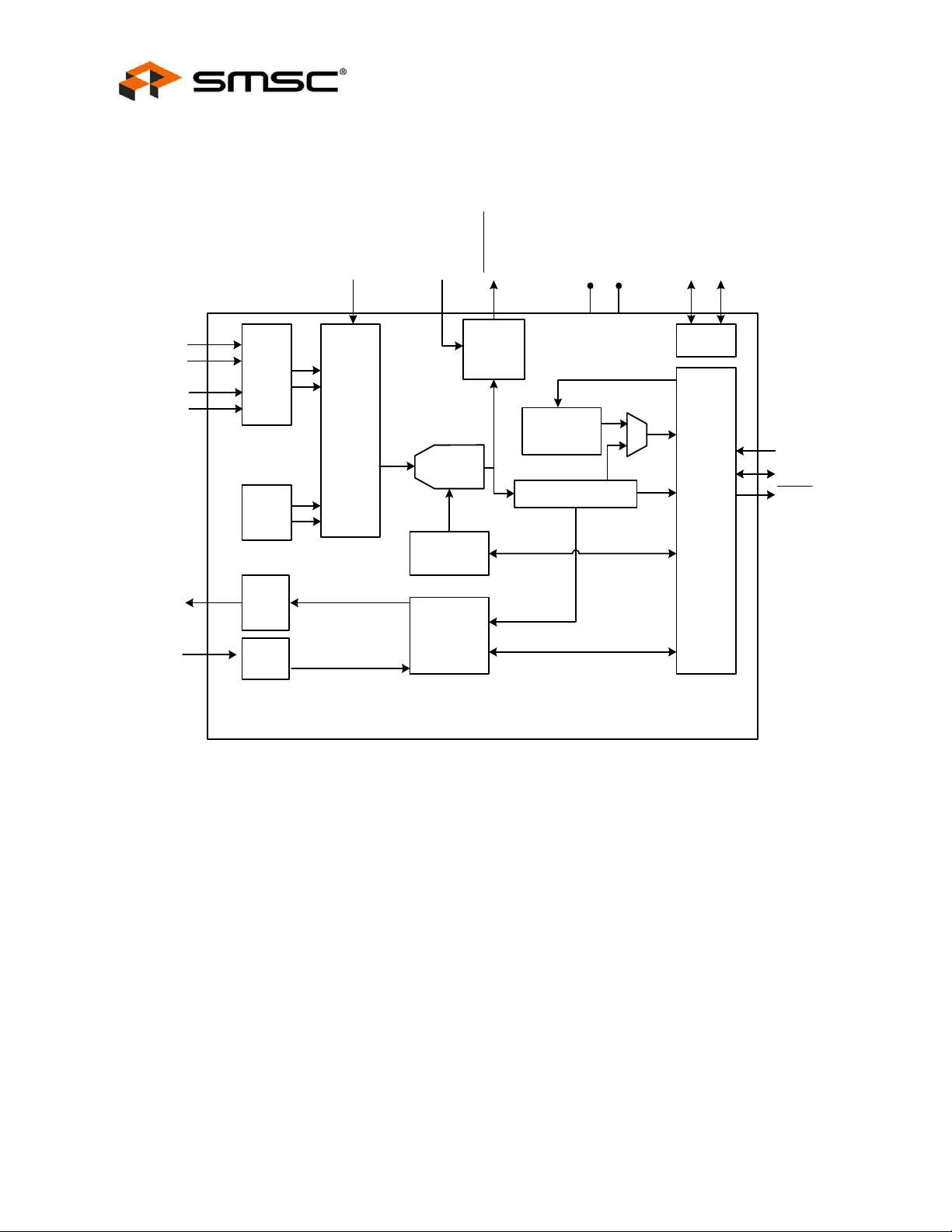
Chapter 1 Block Diagram
TRIP_SET
SHDN_SEL
RPM-Based Fan Controller with HW Thermal Shutdown
VDD
SYS_SHDN
GND
GPIO1*
GPIO2*
Datasheet
DP1
DN1
DP2 / DN3*
DN2 / DP3*
PWM
TACH
External
Temp
Diodes
Analog
Mux
Intern al
Temp
Diode
PWM
driver
Tach
* denote EMC2103-2 pins only
Figure 1.1 EMC2103 Block Diagram
Shutdown
11 bit Σ Δ
ADC
Configuration
Lookup
Table / RPM
Control
Thermal
Logic
Temp Limit
Registers
Temp Registers
GPIO
SMBus
Slave
Protocol
SMCLK
SMDATA
ALERT
Revision 0.85 (01-29-08) 8 SMSC EMC2103
DATASHEET
Page 9
RPM-Based Fan Controller with HW Thermal Shutdown
Datasheet
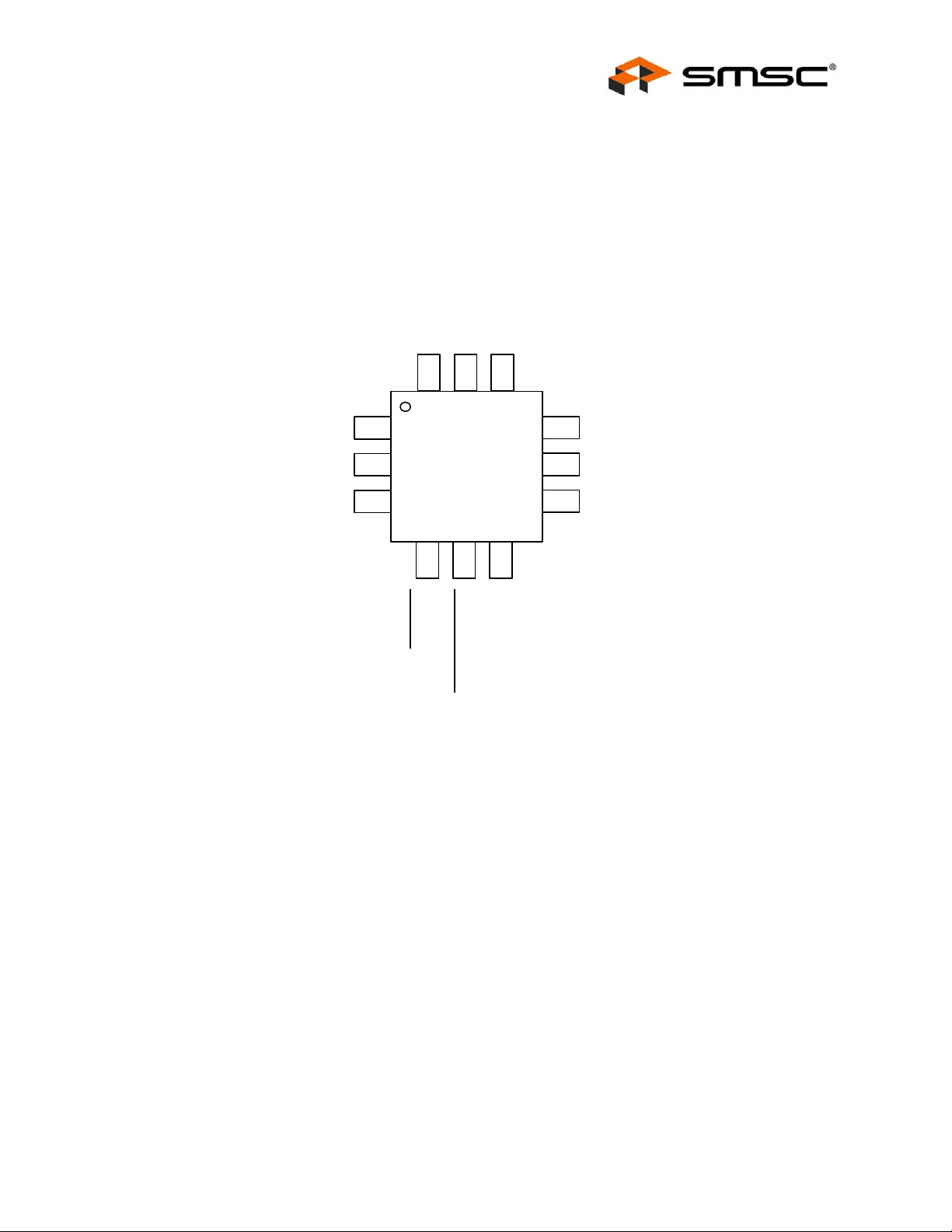
Chapter 2 Pin Layout
DN
DP
VDD
1
2
3
GND
SHDN_SEL
TRIP_SET
12
11
10
EMC2103-1
12-QFN
9
8
7
PWM
TACH
SMCLK
4
5
6
ALERT
SMDATA
SYS_SHDN
Figure 2.1 EMC2103-1 Pin Diagram (12 Pin QFN)
SMSC EMC2103 9 Revision 0.85 (01-29-08)
DATASHEET
Page 10
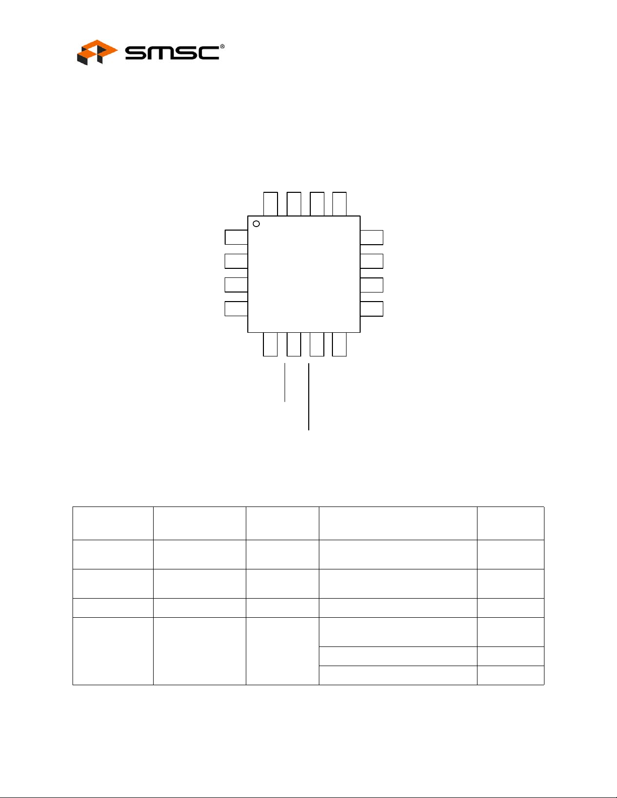
RPM-Based Fan Controller with HW Thermal Shutdown
Datasheet
DN2 / DP3
DP2 / DN3
16
15
TRIP_SET
14
SHDN_SEL
13
PIN NUMBER
EMC2103-1
DN1
DP1
VDD
GPIO1
1
2
3
EMC2103-2
16-QFN
4
5
6
7
8
GPIO2
ALERT
12
11
10
9
GND
PWM
TACH
SMCLK
SMDATA
SYS_SHDN
Figure 2.2 EMC2103-2 Pin Diagram (16 pin QFN)
Table 2.1 Pin Description for EMC2103
PIN NUMBER
EMC2103 -2 PIN NAME PIN FUNCTION PIN TYPE
11DN1
22DP1
3 3 VDD Power Supply Power
N/A 4 GPIO1
Revision 0.85 (01-29-08) 10 SMSC EMC2103
Negative (cathode) analog input for
External Diode 1.
Positive (anode) analog input for
External Diode 1.
GPI1 - General Purpose Input
(default)
GPO1 - Open Drain digital output OD (5V)
GPO1 - Push-pull digital output DO
AIO
AIO
DI (5V)
DATASHEET
Page 11

RPM-Based Fan Controller with HW Thermal Shutdown
Datasheet
Table 2.1 Pin Description for EMC2103 (continued)
PIN NUMBER
EMC2103-1
PIN NUMBER
EMC2103 -2 PIN NAME PIN FUNCTION PIN TYPE
GPI2 - General Purpose Input
(default)
N/A 5 GPIO2
GPO2 - Open Drain digital output OD (5V)
GPO2 - Push-pull digital output DO
4 6 ALERT
Active low interrupt - requires
external pull-up resistor.
Active low Critical / Thermal
5 7 SYS_SHDN
Shutdown output - requires external
pull-up resistor
68SMDATA
79SMCLK
SMBus data input/output - requires
external pull-up resistor
SMBus clock input - requires
external pull-up resistor
8 10 TACH Tachometer input for the Fan DI (5V)
PWM - Open Drain PWM drive
output for the Fan
911PWM
(default)
PWM - Push-Pull PWM drive output
for the Fan
DI (5V)
OD (5V)
OD (5V)
DIOD (5V)
DI (5V)
OD (5V)
DO
10 12 GND Ground connection Power
11 13 SHDN_SEL
12 14 TRIP_SET
Selects the hardware shutdown
channel and operating mode
Voltage input to set the Critical /
Thermal Shutdown threshold
AIO
AIO
Negative (cathode) analog input for
N/A 15 DN2 / DP3
External Diode 2 and positive
(anode) analog input for External
AIO
Diode 3
Positive (anode) analog input for
N/A 16 DP2 / DN3
External Diode 2 and negative
(cathode) connection for External
AIO
Diode 3
The pin type are described in detail below. All pins labelled with (5V) are 5V tolerant.
SMSC EMC2103 11 Revision 0.85 (01-29-08)
DATASHEET
Page 12

RPM-Based Fan Controller with HW Thermal Shutdown
Datasheet
Table 2.2 Pin Types
PIN TYPE DESCRIPTION
Power This pin is used to supply power or ground to the device.
DI
AIO
DO
DIOD
OD
Digital Input - this pin is used as a digital input. This pin is
5V tolerant.
Analog Input / Output - this pin is used as an I/O for analog
signals.
Push / Pull Digital Output - this pin is used as a digital
output. It can both source and sink current.
Digital Input / Open Drain Output this pin is used as an
digital I/O. When it is used as an output, It is open drain
and requires a pull-up resistor. This pin is 5V tolerant.
Open Drain Digital Output - this pin is used as a digital
output. It is open drain and requires a pull-up resistor. This
pin is 5V tolerant.
Revision 0.85 (01-29-08) 12 SMSC EMC2103
DATASHEET
Page 13

RPM-Based Fan Controller with HW Thermal Shutdown
Datasheet
Chapter 3 Electrical Characteristics
Table 3.1 Absolute Maximum Ratings
Voltage on 5V tolerant pins -0.3 to 5.5 V
Voltage on VDD pin -0.3 to 4 V
Voltage on any other pin to GND -0.3 to V
Package Power Dissipation 0.8W up to T
Junction to Ambient (θ
) 50 °C/W
JA
+ 0.3 V
DD
= 85°C W
A
Operating Ambient Temperature Range -40 to 125 °C
Storage Temperature Range -55 to 150 °C
ESD Rating, All Pins, HBM 2000 V
Note: Stresses above those listed could cause permanent damage to the device. This is a stress
rating only and functional operation of the device at any other conditio n above those indicated
in the operation sections of this specification is not implied. When powering this device from
laboratory or system power supplies, it is important that the Absolute Maximum Ratings not be
exceeded or device failure can result. Some power supplies exhibit voltage spikes on their
outputs when the AC power is switched on or off. In addition, voltage transients on the AC
power line may appear on the DC output. If this possibility exi sts, it is suggested that a clamp
circuit be used.
Note: All voltages are relative to ground.
Note: θ
numbers are based on a recommended four 12 mil via s conn ecting the the rma l pad to PCB
JA
ground.
SMSC EMC2103 13 Revision 0.85 (01-29-08)
DATASHEET
Page 14

3.1 Electrical Specifications
Table 3.2 Electrical Specifications
RPM-Based Fan Controller with HW Thermal Shutdown
Datasheet
VDD = 3V to 3.6V, T
= -40°C to 125°C, all Typical values at TA = 27°C unless otherwise noted.
A
CHARACTERISTIC SYMBOL MIN TYP MAX UNIT CONDITIONS
DC Power
Supply Voltage V
DD
33.33.6V
4 Conversions / second, Fan
1.3 1.8 mA
Driver active at maximum PWM
frequency, Dynamic Averaging
Enabled (EMC2103-2)
4 Conversions / second, Fan
Supply Current I
DD
11.5mA
Driver active at maximum PWM
frequency, Dynamic Averaging
Enabled (EMC2103-1)
1 Conversions / second, Fan
450 750 uA
Driver not active, Dynamic
Averaging Disabled
First Conversion
Ready
t
CONV_T
300 ms
Time after power up before all
channels updated
Time before SMBus
SMBus Delay t
SMB_D
10 ms
communications should be sent
by host
External Temperature Monitors
Temperature
±0.5 ±1 °C
Accuracy
±1 ±2 °C -40°C < T
Temperature
Resolution
Diode decoupling
capacitor
Resistance Error
Corrected
C
FILTER
R
SERIES
0.125 °C
2200 2700 pF
100 Ohm
Internal Temperature Monitor
Temperature
Accuracy
Temperature
Resolution
T
DIE
±1 ±2 °C
0.125 °C
PWM Fan Driver
PWM Resolution PWM 256 Steps
PWM Duty Cycle DUTY 0 100 %
TRIP_SET Measurement
Voltage Accuracy V
TRIP
0.5 1 %
60°C < T
30°C < TA < 100°C
DIODE
DIODE
< 125°C
< 125°C
Connected across external
diode, CPU, GPU, or AMD diode
Sum of series resistance in both
DP and DN lines
Revision 0.85 (01-29-08) 14 SMSC EMC2103
DATASHEET
Page 15
RPM-Based Fan Controller with HW Thermal Shutdown
Datasheet
Table 3.2 Electrical Specifications (continued)
VDD = 3V to 3.6V, T
= -40°C to 125°C, all Typical values at TA = 27°C unless otherwise noted.
A
CHARACTERISTIC SYMBOL MIN TYP MAX UNIT CONDITIONS
T emperature Decode
Accuracy
T
TRIP
1 2 °C 5% external resistor
0.5 °C 1% external resistor
RPM Based Fan Controller
Tachometer Range TACH 480 16000 RPM
Tachometer Setting
Accuracy
Δ
TACH
±2.5 ±5 %
Digital I/O pins
Input High Voltage V
Input Low Voltage V
Output High Voltage V
Output Low Voltage V
IH
IL
OH
OL
2.0 V
0.8 V
VDD -
0.4
0.4 V 8 mA current sink
8 mA current drive
V
ALERT and SYS_SHDN pins
Leakage Current I
LEAK
±5 uA
Device powered or unpowered
TA < 85°C
3.2 SMBus Electrical Specifications (Client Mode)
Table 3.3 SMBus Electrical Specifications
VDD= 3V to 3.6V, T
CHARACTERISTIC SYMBOL MIN TYP MAX UNITS CONDITIONS
Input High/Low Current I
Input Capacitance C
Clock Frequency f
Spike Suppression t
Bus free time Start to
Stop
Setup Time: Start t
Setup Time: Stop t
Data Hold Time t
Data Setup Time t
= -40°C to 125°C Typical values are at TA = 27°C unless otherwise noted.
A
SMBus Interface
IH / IIL
IN
410 pF
±5 uA Device powered or unpowered
TA < 85°C
SMBus Timing
SMB
SP
t
BUF
SU:STA
SU:STP
HD:DAT
SU:DAT
10 400 kHz
50 ns
1.3 us
0.6 us
0.6 us
0.6 6 us
0.6 72 us
SMSC EMC2103 15 Revision 0.85 (01-29-08)
DATASHEET
Page 16

RPM-Based Fan Controller with HW Thermal Shutdown
T able 3.3 SMBus Electrical Specifications (continu ed)
VDD= 3V to 3.6V, TA = -40°C to 125°C Typical values are at TA = 27°C unless otherwise noted.
CHARACTERISTIC SYMBOL MIN TYP MAX UNITS CONDITIONS
Datasheet
Clock Low Period t
Clock High Period t
Clock/Data Fall time t
Clock/Data Rise time t
Capacitive Load C
LOW
HIGH
FALL
RISE
LOAD
1.3 us
0.6 us
300 ns Min = 20+0.1C
300 ns Min = 20+0.1C
400 pF Total per bus line
LOAD
LOAD
ns
ns
Revision 0.85 (01-29-08) 16 SMSC EMC2103
DATASHEET
Page 17
RPM-Based Fan Controller with HW Thermal Shutdown
Datasheet
Chapter 4 Communications
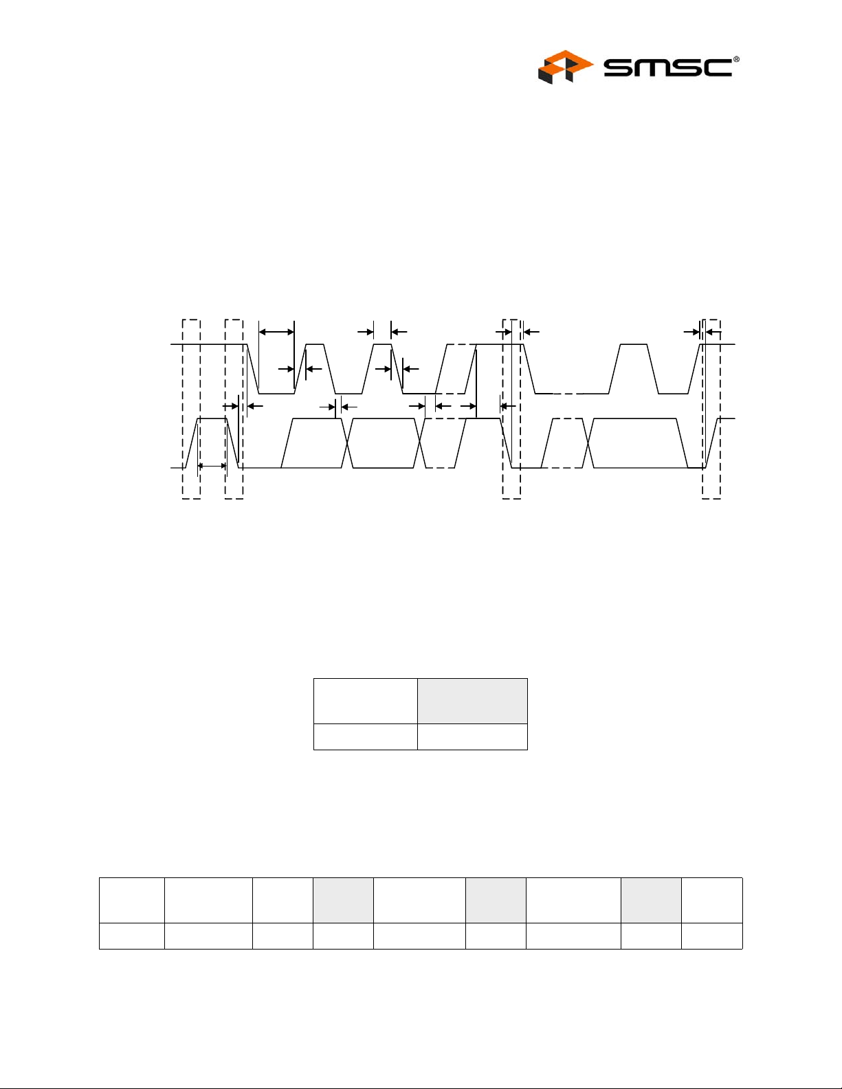
4.1 System Management Bus Interface Protocol
The EMC2103 communicates with a host controller, such as an SMSC SIO, through the SMBus. The
SMBus is a two-wire serial communication protocol between a computer host and its peripheral
devices. A detailed timing diagram is shown in Figure 4.1. Stretching of the SMCLK signal is supported,
however the EMC2103 will not stretch the clock signal.
SMCLK
SMDATA
T
LOW
T
T
HD:STA
T
HD:DAT
T
BUF
P
S
S - Start Condition
RISE
T
HIGH
T
FALL
T
SU:DAT
T
HD:STA
T
SU:STA
S
P - Stop Condition
T
SU:STO
P
Figure 4.1 SMBus Timing Diagram
The EMC2103 contains a single SMBus interface. The EMC2103 client interfaces are SMBus 2.0
compatible and support Send Byte, Read Byte, Receive Byte and the Alert Response Address as valid
protocols. These protocols are used as shown below.
All of the below protocols use the convention in Table 4.1.
Table 4.1 Protocol Format
DATA SENT
TO DEVICE
DATA SENT TO
THE HOST
# of bits sent # of bits sent
4.2 Write Byte
The Write Byte is used to write one byte of data to the registers as shown below Table 4.2:
Table 4.2 Write Byte Protocol
START
SLAVE
ADDRESS WR
ACK
REGISTER
ADDRESS ACK
0 -> 1 0101_110 0 0 0 -> 1 0 XXh 0 1 -> 0
SMSC EMC2103 17 Revision 0.85 (01-29-08)
DATASHEET
REGISTER
DATA ACK STOP
Page 18

4.3 Read Byte
The Read Byte protocol is used to read one byte of data from the registers as show n in Table 4.3.
RPM-Based Fan Controller with HW Thermal Shutdown
Datasheet
Table 4.3 Read Byte Protocol
SLAVE
START
0 -> 1 0101_110 0 0 XXh 0 0 -> 1 0101_110 1 0 XXh 1 1 -> 0
ADDRESS WR
ACK
REGISTER
ADDRESS ACK START
SLAVE
ADDRESS RD ACK
REGISTER
DATA NACK STOP
4.4 Send Byte
The Send Byte protocol is used to set the internal address register pointer to the correct address
location. No data is transferred during the Send Byte protocol as shown in Table 4.4.
Table 4.4 Send Byte Protocol
SLA VE
START
0 -> 1 0101_110 0 0 XXh 1 1 -> 0
ADDRESS WR
ACK
REGISTER
ADDRESS ACK STOP
4.5 Receive Byte
The Receive Byte protocol is used to read data from a register when the internal register address
pointer is known to be at the right location (e.g. set via Send Byte). This is used for consecutive reads
of the same register as shown in Table 4.5.
Table 4.5 Receive Byte Protocol
START
0 -> 1 0101_110 1 0 XXh 1 1 -> 0
SLA VE
ADDRESS RD
ACK REGISTER DATA NACK STOP
4.6 Alert Response Address
The ALERT output can be used as a processor interrupt or as an SMBus Alert when configured to
operate as an interrupt.
When it detects that the ALERT
to the general address of 0001_100b. All devices with active i nterrupts will respond with their client
address as shown in Table 4.6.
Table 4.6 Alert Response Address Protocol
ALERT
START
0 -> 1 0001_100 1 0 0101_1100 1 1 -> 0
Revision 0.85 (01-29-08) 18 SMSC EMC2103
RESPONSE
ADDRESS RD
pin is asserted, the host will send the Alert Response Address (ARA)
ACK
DEVICE
ADDRESS NACK STOP
DATASHEET
Page 19

RPM-Based Fan Controller with HW Thermal Shutdown
Datasheet
The EMC2103 will respond to the ARA in the following way i f the ALERT pin is asserted.
1. Send Slave Address and verify that full slav e address was sent (i.e. the SMBus communication
from the device was not prematurely stopped due to a bus contention event).
2. Set the MASK bit to clear the ALERT pin.
4.7 SMBus Address
The EMC2103 SMBus Address is fixed at 0101_110xb.
Other addresses are available. Contact SMSC for details.
Attempting to communicate with the EMC2103 SMBus interface with an invalid slave address or invalid
protocol will result in no response from the devi ce and will not affect its register contents.
4.8 SMBus Time-out
The EMC2103 includes an SMBus time-out feature. Following a 30ms period of inactivity on the
SMBus, the device will time-out and reset the SMBus interface.
SMSC EMC2103 19 Revision 0.85 (01-29-08)
DATASHEET
Page 20
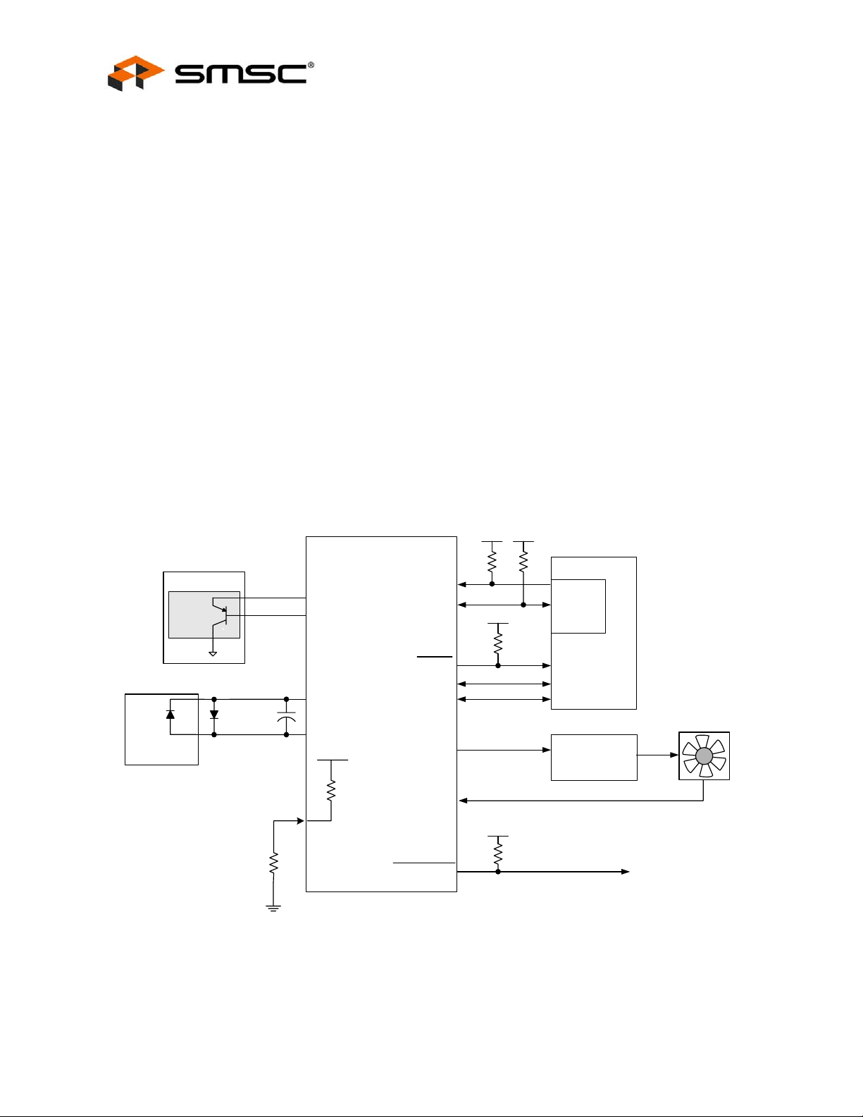
Chapter 5 General Description
The EMC2103 is an SMBus compliant fan controller with one external (EMC2103-2 offers up to three
external diode channels) and one internal temperature channels. The fan driver can be operated using
two methods each with two modes. The methods include an RPM based Fan Speed Control Algorithm
and a direct PWM drive setting. The modes include manually programming the desired settings or
using the internal programmable temperature look-up table to select the desired setting based on
measured temperature.
The temperature monitors offer 1°C accuracy (for external diodes) with sophisticated features to
reduce errors introduced by series resistance and beta variation of substrate the rmal diode transistors
commonly found in processors (including support of the BJT o r transistor model for a CPU diode).
The EMC2103 allows the user to program temperatures generated from external sources to control
the fan speed. This functionality also supports DTS data from the CPU. By pushing DTS or standard
temperature values into dedicated registers, the external temperature readings can be used in
conjunction with the external diode(s) and interna l diode to control the fan speed.
The EMC2103 also includes a hardware programmable temperature limit and dedicated system
shutdown output for thermal protection of critical circuitry.
Figure 5.1 shows a system diagram of the EMC2103.
RPM-Based Fan Controller with HW Thermal Shutdown
Datasheet
Thermal
diode
Optional antiparallel diode
CPU
* denotes EMC2103-2 only
EMC2103
DP1
DN1
DP2 / DN3*
DN2 / DP3*
1.5V
1.2k
TRIP_SET
SYS_SHDN
SMCLK
SMDATA
ALERT
GPIO1*
GPIO2*
PWM
TACH
VDD VDD
Figure 5.1 System Diagram for EMC2103
VDD
VDD
HOST
SMBus
Interface
Fan Drive
Circuitry
Revision 0.85 (01-29-08) 20 SMSC EMC2103
DATASHEET
Page 21
RPM-Based Fan Controller with HW Thermal Shutdown
Datasheet
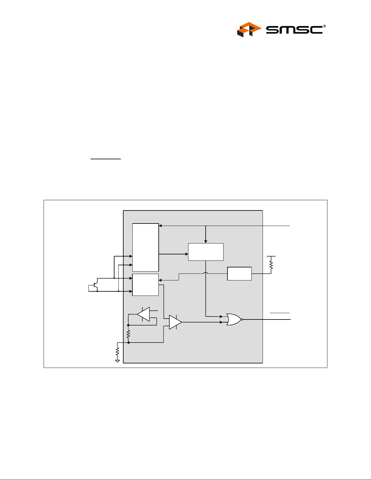
5.1 Critical/Thermal Shutdown
The EMC2103 provides a hardware Critical/Thermal Shutdown function for systems. Figure 5.2 is a
block diagram of this Critical/Thermal Shutdown function. The Critical/Thermal Shutdown function
accepts configuration information from the fixed states of the SHDN_SEL pin as described in
Section 5.1.1.
Each of the software programmed temperature limits can be optionally co nfigured to act as inputs to
the Critical / Thermal Shutdown independent of the hardware shutdown operation. When configured to
operate this way, the SYS_SHDN# pin will be asserted when the temperature meets or exceeds the
limit. The pin will be released when the temperature drops below the limit however the individual status
bits will not be cleared if set (see Section 6.13).
The analog portion of the Critical/Thermal Shutdown function monitors the hardware determined
shutdown channel (see Section 5.1.1). This measured temperature is then compared with TRIP_SET
point. This TRIP_SET point is set by the system designer with a single external resistor divider as
described in Section 5.1.2.
The SYS_SHDN is asserted when the indicated temperature meets or exceeds the temperature
threshold (TP) established by the TRIP_SET input pin for a number of consecutive measurements
defined by the fault queue. If the HW_SHDN output is asserted an d the temperature drops below the
threshold, then it will be set to a logic ‘0’ state.
H/W Thermal
Shutdown Sensor
TRIP_SET
Critical / Thermal Shutdown
Temperature
Conversion
Temperature
Conversion
Figure 5.2 Block Diagram of Critical / Thermal Shutdown
Software
Shutdown Enable
SW_SHDN
HW_SHDN
Resistor
Decode
SMBus
Traffic
VDD
SHDN_SEL
SYS_SHDN
SMSC EMC2103 21 Revision 0.85 (01-29-08)
DATASHEET
Page 22

5.1.1 S HDN_SEL Pin
The EMC2103 has a ‘strappable’ input (SHDN_SEL) allowing for configuration of the hardware
Critical/Thermal Shutdown input channel. The pull-up resistor used on this pin identifies which
configuration setting is used as shown in Table 5.1.
.
PULL UP RESISTOR MODE OF OPERATION CONFIGURATION MECHANISM
RPM-Based Fan Controller with HW Thermal Shutdown
Datasheet
Table 5.1 SHDN_SEL Pin Decode
4.7k Ohm
<
6.8k Ohm
10k Ohm
15k Ohm Internal Diode Host control via SMBus
22k Ohm
>
33k Ohm
Note 5.1 For the EMC2103-1, the decode for a 22k Ohm resistor on the SHDN_SEL pin will be to
use the External Diode 1 channel in Diode Mode (the same as the decode for a 6.8k Ohm
resistor) as the hardware shutdown device.
5.1.2 TRIP_SET Pin
External Diode 1 Simple Mode Beta compensation disabled, REC
disabled - recommended for AMD
CPU diodes
External Diode 1 Diode Mode Beta compensation disabled, REC
enabled
External Diode 1 Transistor Mode Beta compensation enabled, REC
enabled - recommended for Intel
45nm and 65mn CPU diodes
External Diode 2 Transistor Mode Beta Compensation enabled, REC
enabled (EMC2103-2 only) See
Note 5.1
External Diode 1 Transistor Mode Beta compensation enabled, REC
enabled
Host control via SMBus
Host control via SMBus
Host control via SMBus
Host control via SMBus
Host control via SMBus
The EMC2103’s TRIP_SET pin is an analog input to the Critical/Thermal Shutdown block which sets
the Thermal Shutdown temperature. The system designer creates a voltage level at the input through
a simple resistor connected to GND as shown in Figure 5.2. The value of this resistor is used to create
an input voltage on the TRIP_SET pin which is translated into a temperature ranging from 65°C to
127°C as shown in Table 5.2
APPLICATION NOTE: Current only flows when the TRIP_SET pin is being mon itored. At all othe r ti mes, the intern al
reference voltage is removed and the TRIP_SET pin will be pul led down to ground.
APPLICATION NOTE: The TRIP_SET pin circuitry is designed to use a 1% resistor externally. Using a 1% resistor
will result in the Thermal / Critical Shutdown temperature being decoded correctly. If a 5%
resistor is used, then the Thermal / Critical Shutdown temperature may be decoded with as
much as ±1°C error.
Revision 0.85 (01-29-08) 22 SMSC EMC2103
DATASHEET
Page 23

RPM-Based Fan Controller with HW Thermal Shutdown
Datasheet
Table 5.2 TRIP_SET Resistor Setting
T
(°C) RSET (1%) T
TRIP
65 0.0 97 1240
66 28.7 98 1330
67 48.7 99 1400
68 69.8 100 1500
69 90.9 101 1580
70 113 102 1690
71 137 103 1820
72 158 104 1960
73 182 105 2050
74 210 106 2210
75 237 107 2370
(°C) RSET (1%)
TRIP
76 261 108 2550
77 294 109 2740
78 324. 110 2940
79 348 111 3160
80 383 112 3480
81 412 113 3740
82 453 114 4120
83 487 115 4530
84 523 116 4990
85 562 117 5490
86 604 118 6040
87 649 119 6810
88 698 120 7870
89 750 121 9090
90 787 122 10700
91 845 123 12700
92 909 124 15800
93 953 125 20500
94 1020 126 29400
95 1100 127 49900
96 1150 65 Open
SMSC EMC2103 23 Revision 0.85 (01-29-08)
DATASHEET
Page 24

5.2 Fan Control Modes of Operation
The EMC2103 has four modes of operation for the fa n driver. Each mode uses Ramp Rate control and
the Spin Up Routine
1. PWM Setting Mode - in this mode of operation, the user directly controls the PWM duty cycle
setting. Updating the Fan Driver Setting Register (see Section 6.20) will instantly update the fan
drive.
This is the default mode. The PWM Setti ng Mode is enabled by clearing both the EN_ALGO
bit in the Fan Configuration Register (see Section 6.22) and the LUT_LOCK bit in the Look
Up Table Config uration Register (see Section 6.32).
Whenever the PWM Setting Mode is enabled the current drive will be changed to what was
last written into the Fan Driver Setting Register.
2. Fan Speed Control Mode (FSC) - in this mode of operation, th e user determines a fan speed and
the drive setting is automatically updated to achieve this target speed.
This mode is enabled by clearing the L UT_LOCK bit in the Look Up Table (LUT)
Configuration Register and setting the EN_ALGO bit in the Fan Configuration Register.
3. Using the Look Up Table with Fan Drive Settings (PWM Setting w/ LUT Mode) - In this mode of
operation, the user programs the Look Up Table with PWM duty cycle settings and corresponding
temperature thresholds. The fan drive is set based on the measured temperatures and the
corresponding drive settings.
This mode is enabled by programming the L ook Up Table then setting the LUT_LOCK bit
while the RPM / PWM bit is set to a ‘1’ (see Section 6.32)
RPM-Based Fan Controller with HW Thermal Shutdown
Datasheet
4. Using the Look Up Table with Fan Speed Control algorithm (FSC w/ LUT Mode)- In this mode of
operation, the user programs the Look Up Table with fan speed target values and corresponding
temperature thresholds. The TACH Target Register will be set based on the measured
temperatures and the corresponding target settings. The PWM drive settings will be determined
automatically based on the RPM based Fan Speed Control Algorithm
This mode is enabled by programming the L ook Up Table then setting the LUT_LOCK bit
while the RPM / PWM bit is set to ‘0’ (see Section 6.32).
Table 5.3 Fan Controls Active for Operating Mode
DIRECT PWM
SETTING MODE FSC MODE
Fan Driver Setting (read
/ write)
Fan Driver Setting (read
only)
EDGES[1:0] EDGES[1:0]
(Fan Configuration)
- RANGE[1:0]
(Fan Configuration)
UPDATE[2:0]
(Fan Configuration)
LEVEL
(Spin Up Configuration)
UPDATE[2:0]
(Fan Configuration)
LEVEL
(Spin Up Configuration)
DIRECT PWM SETTING W/
LUT MODE FSC W/ LUT MODE
Fan Driver Setting (read only) Fan Driver Setting (read
only)
EDGES[1:0] EDGES[1:0]
- RANGE[1:0]
(Fan Configuration)
UPDATE[2:0]
(Fan Configuration)
LEVEL
(Spin Up Configuration)
UPDATE[2:0]
(Fan Configuration)
LEVEL
(Spin Up Configuration)
SPINUP_TIME[1:0]
(Spin Up Configuration)
SPINUP_TIME[1:0]
(Spin Up Configuration)
SPINUP_TIME[1:0]
(Spin Up Configuration)
SPINUP_TIME[1:0]
(Spin Up Configuration)
Fan Step Fan St ep Fan Step Fan Step
- Fan Minimum Drive Fan Minimum Drive
Revision 0.85 (01-29-08) 24 SMSC EMC2103
DATASHEET
Page 25

RPM-Based Fan Controller with HW Thermal Shutdown
Datasheet
Table 5.3 Fan Controls Active for Operating Mode (continued)
DIRECT PWM
SETTING MODE FSC MODE
Valid TACH Count Valid TACH Count Valid TACH Co unt Valid TACH Count
- TACH Target (read /
write)
TACH Reading TACH Reading TACH Reading TACH Reading
- - Look Up Table Drive /
- DRIVE_FAIL_CNT [1:0]
(Spin Up Configuration) +
Fan Drive Fail Band
DIRECT PWM SETTING W/
LUT MODE FSC W/ LUT MODE
- TACH Target (read only)
Tempe rature Settings (read
only)
- DRIVE_FAIL_CNT [1:0]
Look up Table Drive /
Temperature Settings
(read only)
(Spin Up Configuration)
+ Fan Drive Fail Band
5.3 PWM Fan Driver
The EMC2103 supports a high or low frequency PWM driver. The output can be configured as either
push-pull or open drain and the frequency ranges from 9.5Hz to 26kHz in four programmable
frequency bands.
5.4 Fan Control Look-Up Table
The EMC2103 uses a look-up table to apply a user-programmable fan control profile based on
measured temperature to the fan driver. In this look-up table, each temperature channel is allowed to
control the fan drive output independently (or jointly) by programming up to eight pairs of temperature
and drive setting entries.
The user programs the look-up table based on the desired operation. If the RPM based Fan Speed
Control Algorithm is to be used (see Section5.5), then the user must program a fan spee d target for
each temperature setting of interest. Alternately, if the RPM based Fan Speed Control Algorithm is not
to be used, then the user must program a PWM setting for each temperature setting of interest.
If the measured temperature on the External Diode channel meets or exceeds any of the temperature
thresholds for any of the channels, the fan output will be automatically set to the desired setting
corresponding to the exceeded temperature. In cases where multiple te mperature channel thresholds
are exceeded, the highest fan drive setting will take precedence. Figure 5.3 shows an example of this
behavior using a single channel.
When the measured temperature drops to a point below a lower threshold minus the hysteresis value,
the fan output will be set to the corresponding lower set point.
SMSC EMC2103 25 Revision 0.85 (01-29-08)
DATASHEET
Page 26
RPM-Based Fan Controller with HW Thermal Shutdown
Datasheet
Fan
Temp
Setting
T6
T6 - Hyst
T5
T5 - Hyst
T4
T4 - Hyst
T3
T3 - Hyst
T2
T2 - Hyst
T1
Averaged
Temperature
Fan
Setting
Measurement taken
Time
Figure 5.3 Fan Control Look-Up Table Example
S6
S5
S4
S3
S2
S1
5.4.1 P rogramming the Look Up Table
When the Look Up Table is used, it must be loaded and configured correctly based on the system
requirements. The following steps outline the procedure.
1. Determine whether the Look Up Table will drive a PWM duty cycle or a tachometer target value
and set the RPM / PWM bit in the Fan LUT Configuration Register (see Section 6.32).
2. Determine which mea surement channels (up to four) are to be used with the Look Up Table a nd
set the TEMP3_CFG and TEMP4_CFG bits accordingly in the Fan LUT Co nfiguration Register.
3. Fo r each step to be used in the LUT, set the Fan Setting (either PWM or TACH Target as set by
the RPM / PWM bit). If a setting is not used, then set it to FFh (if a PWM) or 00h (if a TACH Target).
Load the lowest settings first in ascending order (i.e. Fan Se tting 1 is the lowest setting greater
than “off”. Fan Setting 2 is the next highest setting, etc.). See Section 6.33.
4. For each step to be used in the LUT, set each of the measurement channel thresholds. These
values must be set in the same data format that the data is presented. If DTS is to be used, then
the format should be in temperature with a maximum threshol d of 100°C (64h). If a measurement
channel is not used, then set the threshold at FFh.
5. Update the thresh old hysteresis to be smaller than the smallest table step.
6. Con figure the RPM based Fan Speed Control Algorithm if it is to be used. See Section 5.5.1 for
more details.
Revision 0.85 (01-29-08) 26 SMSC EMC2103
DATASHEET
Page 27

RPM-Based Fan Controller with HW Thermal Shutdown
Datasheet
7. Set the LUT_LOCK bit to enable the Look Up Table and begin fan control in the Fan LUT
Configuration Register.
5.4.2 D TS Support
The EMC2103 supports DTS (Intel’s Digital Temperature Sensor) data in the Fan Control Look Up
Tabl e. Intel’s DTS data is a positive number that represents the processor’s relative temperature below
a fixed value called T
CONTROL
example, a DTS value of 10°C means that the actual processor temperature is 10°C below T
or equal to 90°C.
Either or both of the Pushed Temperature Registers can be written with DTS data and used to control
the fan driver. When DTS data is entered, then the USE_DTS_Fx bit must be set in the Fan LUT
Configuration register. Once this bit is set, the DTS data entered is automatically subtracted from a
value of 100°C. This delta value is then used in the Look Up Table as standard temperature data.
which is generally equal to 100°C for Intel Mobile processors. For
CONTROL
APPLICATION NOTE: The device is designed with the assumption that T
CONTROL
is 100°C. As such, all DTS
related conversions are done based on this value including Look Up Table comparisons. If
T
CONTROL
is adjusted (i.e. T
CONTROL
thresholds should be adjusted by a value equal to T
is shifted to 105°C), then all of the Look Up Table
CONTROL
- 100°C.
5.5 RPM based Fan Speed Control Algorithm (FSC)
The EMC2103 includes an RPM based Fan Speed Control Algorithm.
This fan control algorithm uses Proportional, In tegral, and Derivative terms to automatically approach
and maintain the system’s desired fan speed to an accuracy directly proportional to the accuracy of
the clock source. Figure 5.4 shows a simple flow diagram of the RPM based Fan Speed Control
Algorithm operation.
The desired tachometer count is set by the user inputting the desired number of 32.768KHz cycles
that occur per fan revolution. This is done by either manually setting the TACH Target Register or by
programming the Temperature Look-Up Table. The user may change the target count at any time. The
user may also set the target count to FFh in order to disable the fan driver for lower cu rrent operation.
For example, if a desired RPM rate for a 2-pole fan is 3000 RPM then the user would input the
hexidecimal equivalent of 1296 (51h in the TACH Target Register). This number represents the number
of 32.768KHz cycles that would occur during the time it takes the fan to complete a single revolution
when it is spinning at 3000RPMs. See Section 6.30 for RPM -> TACH calculations or Appendix B for
a complied table showing this information (for default conditions).
The EMC2103’s RPM based Fan Speed Control Algorithm has programmable configuration settings
for parameters such as ramp-rate control and spin up conditions. The fan driver automatically detects
and attempts to alleviate a stalled/stuck fan condition while also asserting the ALERT
EMC2103 works with fans that operate up to 16,000 RPMs and provi des a valid tachometer signal.
pin. The
SMSC EMC2103 27 Revision 0.85 (01-29-08)
DATASHEET
Page 28

Set TACH Target
Count
Measure Fan Speed
RPM-Based Fan Controller with HW Thermal Shutdown
Datasheet
Ma in tain F an Driv e
Spin Up
Required
?
No
Yes
Yes
Reduce Fan Drive In c re a se F a n D riv e
TACH
Reading =
TACH
Target?
TACH
Reading <
TACH
Target?
Yes
No
No
Perform Spin Up
Routine
Ra mp Ra te Co ntr ol
Figure 5.4 RPM based Fan Speed Control Algorithm
5.5.1 P rogramming the RPM Based Fan Speed Control Algorithm
The RPM based Fan Speed Control Algorithm powers-up disabled. The following registers control the
algorithm. The EMC2103 fan control registers are pre-loaded with defaults that will work for a wide
variety of fans so only the TACH Target Register is required to set a fan speed. The other fan control
registers can be used to fine-tune the algorithm behavior based on application requirements.
Note that steps 1 - 7 are optional and need only be performed if the default settings do not provide
the desired fan response.
1. Set the Valid TACH Count Register to maximum number of tach counts to indicate the fan is
spinning.
2. Set th e Spin Up Configuration Register to the Spin Up Level and Spin Time desired.
Revision 0.85 (01-29-08) 28 SMSC EMC2103
DATASHEET
Page 29

RPM-Based Fan Controller with HW Thermal Shutdown
Datasheet
3. Set the F an Step Register to the desired step size.
4. Set the F an Minimum Drive Register to the minimum drive value that will maintain fan operation.
5. Set th e Update Time, and Edges options in the Fan Configuration Register.
6. Set th e valid TACH count setting at the highest count that indicates that the fan is spinning.
7. Set the TACH Targe t Register to the desired tachometer count.
8. Enable the RPM based Fan Speed Control Algorithm by setting the EN_ALGO bit.
5.6 Tachometer Measurement
The tachometer measurement circuitry is used in conjunction with the RPM based Fan Speed Control
Algorithm to update the fan driver output. Additionally, it can be used in Direct Setting mode as a
diagnostic for host based fan control.
This method monitors the TACH signal in real time. It constantly updates the tachometer measurement
by reporting the number of clocks between a user progra mmed number of edges on the TACH signal
(see Table 8.5)
Using the Tach Period Measurement method provides fast response times for the RPM based Fan
Speed Control Algorithm and the data is presented as a count value that represents the fan RPM
period. When this method is used, all fan target values must be input as a count value for proper
operation.
APPLICATION NOTE: The Tach Period Measurement method works independently of the drive settings. If the
device is put into Direct Setting and the fan drive is set at a level that i s lower than the fan
can operate (including zero drive), then the tachometer measurement may signal a Stalled
Fan condition and assert an interrupt.
5.6.1 Stalled Fan
A Stalled fan is detected differently based on which tach method is enabled. If the Tach Period
Measurement measurement method is implemented, and if the tach counter exceeds the userprogrammable Valid TACH Count setting then it will flag the fan as stalled and trigger an interrupt.
If the RPM based Fan Speed Control Algorithm is enabled, the algorithm will automatically attempt to
restart the fan until it detects a valid tachometer level or is disabled.
The FAN_STALL Status bit indicates that a stalled fan was detected. This bit is checked conditionally
depending on the mode of operation.
When the Direct Setting Mode or Direct Setting with LUT Mode are enabled or the Spin Up Routine
is initiated, the FAN_STALL interrupt will be masked for the duration of the programmed Spin Up
Time (see Table 8.16). This is to allow the fan opportunity to reach a valid speed without generating
unnecessary interrupts.
When the Direct Setting Mode or Direct Setting w/ LUT Mode are activa ted then whenever the
TACH Reading Register value exceeds the Va lid TACH Count Register setting, the FAN_STALL
status bit will be set.
When using the RPM based Fan Speed Control Algorithm (either FSC Mode or LUT with FSC
Mode), the stalled fan condition is checked whenever the Update Time is met and the fan drive
setting is updated. It is not a continuous check.
5.6.2 A ging Fan or Invalid Drive Detection
The EMC2103 contains circuitry that detects that the programmed fan speed can be reached b y the
fan. If the target fan speed cannot be reached within a user defined band o f tach counts at maximum
drive then the DRIVE_FAIL status bit is and the ALERT
fan conditions (where the fan’s natural maximum speed degrades over time) or incorrect fan speed
settings.
SMSC EMC2103 29 Revision 0.85 (01-29-08)
pin is asserted. This is useful to detect aging
DATASHEET
Page 30

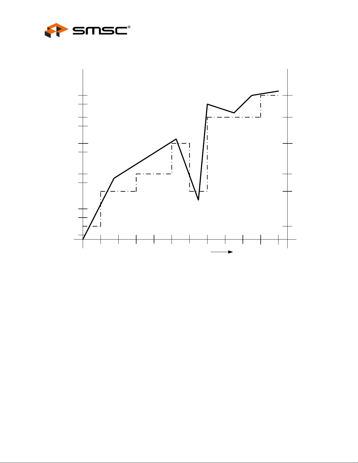
5.7 Spin Up Routine
The EMC2103 also contains programmable circuitry to control the spin up behavior of the fan driver
to ensure proper fan operation. The Spin Up Routine is initiated under the following conditions when
the Tach Period Measurement method of tach measurement is used. This applies to either the RPM
based Fan Speed Control Algorithm mode or the Direct Setting mode (with or without the Look Up
Table).
1. The TACH Target Register value changes from a value of FFh to a value that is less than the Valid
TACH Count (see Section 8.10 and Section 8.12).
2. Th e RPM based Fan Speed Control Algorithm’s measured TACH Reading Register value is greater
than the Valid TACH Count setting.
When the Spin Up Routine is operating, the fan driver is set to full scale (optional) for one quarter of
the total user defined spin up time. For the remaining spin up time, the fa n driver output is set a a user
defined level (30% through 65% drive).
After the Spin Up Routine has finished, the EMC2103 measures the TACH signal. If the measured
TACH Reading Register value is higher than the Valid TACH Count Register setting, the FAN_SPIN
status bit is set and the Spin Up Routine will automatically attempt to restart the fan.
Figure 5.5 shows an example of the Spin Up Routine in response to a programmed fan speed change
based on the first condition above.
RPM-Based Fan Controller with HW Thermal Shutdown
Datasheet
Prev Target
Count = FFh
Target Count
Changed
100%
(optional)
30% through 65%
¼ of Spin U p T im e
Spin Up Time
New Target Count
Update Time
Check TACH
Figure 5.5 Spin Up Routine
Fan Step
Algorithm controlled drive
Target Count
Reached
Revision 0.85 (01-29-08) 30 SMSC EMC2103
DATASHEET
Page 31

RPM-Based Fan Controller with HW Thermal Shutdown
Datasheet
5.8 Ramp Rate Control
The PWM output drive can be configured with automatic ramp rate control. If the RPM based Fan
Speed Control Algorithm is used, then this ramp rate control is automatically used based on the fan
control derivative option settings. See Section 6.23, "Fan Configuration 2 Register". The user programs
a maximum step size for the PWM setting and an update time. The update time varies from 100ms to
1.6s while the PWM maximum step can vary from 1 PWM count to 31 PWM counts.
When a new PWM is entered, the delta from the next PWM and the previous PWM is determined. If
this delta is greater than the Max Step settings, then the PWM is incrementally adjusted every 100ms
to 1.6s as determined by the Update Time until the target PWM setting is reached. See Figure 5.6.
Next Desired
Setting
Previous
Setting
Max
Step
Max
Step
Setting Changed
5.9 Watchdog Timer
The EMC2103 contains an internal Watchdog Timer. Once the device has powered up the watchdog
timer monitors the bus traffic for signs of activity. The Watchdog Timer starts when the internal supply
has reached its operating point. The Watchdog Timer only starts immediately after power-up and once
it has been triggered or deactivated will not restart.
If four (4) seconds elapse without the system host programming the device, then the watchdog will be
triggered and the following will occur:
1. The WATCH status bit will be set.
2. The fan driver will be set to full scale drive. It will remain at full scale drive until one of the three
conditions listed below are met.
If the Watchdog Timer is triggered, the following three operations will disable the timer and return the
device to normal operation. Alternately, if the Watchdog Timer has not yet been triggered performing
any one of the following will disable it.
1. Writing the Fan Setting Register will disable the Watchdog Timer.
2. Enabling the RPM based Fan Speed Control Algorithm by setting the EN_ALGO bit will disable the
Watchdog Timer. The fan d river will be set based on the RPM based Fan Speed Control Algorithm.
Update
Time
Figure 5.6 Ramp Rate Control
Update
Time
SMSC EMC2103 31 Revision 0.85 (01-29-08)
DATASHEET
Page 32

RPM-Based Fan Controller with HW Thermal Shutdown
Datasheet
3. Setti ng the LUT_LOCK bit will disable th e Watchdog Timer. The fan driver will be set based on the
Look Up Table settings.
Writing any other configuration registers will not disable the Watchdog Timer.
APPLICATION NOTE: Disabling the Watchdog will not automatically set the fa n drive. This must be done manually
(or via the Look Up Table).
5.10 Fault Queue
The EMC2103 contains a programmable fault queue on all fault cond itions. The fault queue defines
how many consecutive out-of-limit conditions must be reported before the correspond ing status bit is
set (and the ALERT pin asserted).
5.11 Temperature Monitoring
The EMC2103 can monitor the temperature of up to three (3) externally connected diodes as well as
the internal or ambient temperature. Each channel is configure d with the following features enable d or
disabled based on user settings and system requirements.
5.11.1 Dynamic Averaging
The EMC2103 supports dynamic averaging. When enable d, this feature changes the conversion time
for all channels based on the selected conversion rate. This essentially increases the averaging factor
as shown in Table 5.4. The benefits of Dynamic Averaging are improved noise rejection due to the
longer integration time as well as less random variati on on the temperature measurement.
Table 5.4 Dynamic Averaging Behavior
AVERAGING FACTOR (RELATIVE TO 11-BIT CONVERSI0N)
CONVERSION RATE
1 / sec 8x 1x
2 / sec 4x 1x
4 / sec 2x 1x
Continuous 1x 1x
5.11.2 Resistance Error Correction
The EMC2103 includes active Resistance Error Correction to remove the effect of up to 100 ohms of
series resistance. Without this automatic feature, voltage developed across the parasitic resistance in
the remote diode path causes the temperature to read higher than the true temperature is. The error
induced by parasitic resistance is approximately +0.7°C per ohm. Sources of parasitic resistance
include bulk resistance in the remote temperature transistor junctio ns, series resistance in the CPU,
and resistance in the printed circuit board traces and package leads. Resistance error correction in the
EMC2103 eliminates the need to characterize and compensate for parasitic resistance in the remote
diode path.
DYNAMIC AVERAGING
ENABLED
DYNAMIC AVERAGING
DISABLED
Revision 0.85 (01-29-08) 32 SMSC EMC2103
DATASHEET
Page 33

RPM-Based Fan Controller with HW Thermal Shutdown
Datasheet
5.11.3 Beta Compensation
The forward current gain, or beta, of a transistor is not constant as emitter currents change. As well,
it is not constant over changes in temperature. The variation in beta causes an error in temperature
reading that is proportional to absolute temperature. This correction is done by implementin g the BJT
or transistor model for temperature measurement.
For discrete transistors configured with the collector and base shorted together, the beta is generally
sufficiently high such that the percent change in beta variation is very small. For example, a 10%
variation in beta for two forced emitter currents with a transistor whose ideal beta is 50 would contri bute
approximately 0.25°C error at 100°C. However for substrate transistors where the base-emitter junction
is used for temperature measurement and the collector is tied to the substrate, the proportional beta
variation will cause large error. For example, a 10% variation in beta for two forced emitter currents
with a transistor whose ideal beta is 0.5 would contribute approximately 8.25°C error at 100°C.
The Beta Compensation circuitry in the EMC2103 corrects for this beta variation to eliminate any error
which would normally be induced. It automatically detects the appropriate beta setting to use.
5.11.4 Digital Averaging
The external diode channels support a 4x digital averaging filter. Every cycle, this filter updates the
temperature data based an a running average of the last 4 measured temperature values. The digital
averaging reduces temperature flickering and increases temp erature measurement stability.
The digital averaging can be disabled by setting the DIS_AVG bit in the Configuration 2 Register (see
Section 6.11).
5.12 Diode Connections
The External Diode 1 channel can support a diode-connected transistor (such as a 2N3904) or a
substrate transistor requiring the BJT or transistor model (such as those found in a CPU or GPU) as
shown in Figure 5.7.
The External Diode 2 channel supports any diode connection shown or it can be configured to operate
in anti-parallel diode (APD) mode. When configured in APD mode, a third temperature channel is
available that shares the DP2 and DN2 pins. When in this mode, both the external diode 2 channel
and external diode 3 channel thermal diodes must be conn ected as diodes.
to
DP
to
DN
Local Ground
to
DP
to
DN
to
DP
to
DN
Typical remote
substrate transistor
i.e. CPU substrate PNP
SMSC EMC2103 33 Revision 0.85 (01-29-08)
Typical remote
discrete PNP transistor
i.e. 2N3906
Figure 5.7 Diode Connections
Typical remote
discrete NPN transistor
i.e. 2N3904
DATASHEET
Page 34

5.12.1 Diode Faults
The EMC2103 actively detects an open and short conditio n on each measurement channel. When a
diode fault is detected, the temperature data MSByte is forced to a value of 80h and the FAULT bit is
set in the Status Register. When the External Diode 2 channel is configured to operate in APD mode,
the circuitry will detect independent open fault conditions, however a short condition will be shared
between the External Diode 2 and External Diode 3 channels.
If a diode fault occurs on the hardware defined sh utdown channel, then no temperature comparison is
performed. The SYS_SHDN
5.13 GPIOs
The EMC2103-2 contains two dedicated GPIO pins. The GPIO pins can be in dividually configured as
an input or an output and as a push-pull or open-drain output. Additionally, each GPIO pin, when
configured as an input, can be individually enabled to trigge r an interrupt when they change states.
RPM-Based Fan Controller with HW Thermal Shutdown
Datasheet
pin will not be asserted.
Revision 0.85 (01-29-08) 34 SMSC EMC2103
DATASHEET
Page 35

RPM-Based Fan Controller with HW Thermal Shutdown
Datasheet
Chapter 6 Register Set
6.1 Register Map
The following registers are accessible through the SMBus Interface. All register bits marked as ‘-’ will
always read ‘0’. A write to these bits will have no effect.
APPLICATION NOTE: All registers denoted with a ** are specific to the EMC2103-2 only. Writing to these registers
by the EMC2103-1 will have no affect and reading from them will return ‘00h’.
Table 6.1 EMC2103 Register Set
ADDR R/W
00h R Internal Temp
01h R Internal Temp
02h R External Diode 1
03h R External Diode 1
04h ** R External Diode 2
05h ** R External Diode 2
06h ** R External Diode 3
REGISTER
NAME FUNCTION
Reading High
Byte
Reading Low Byte
Temp Re ading
High Byte
Temp Re ading
Low Byte
Temp Re ading
High Byte **
Temp Re ading
Low Byte **
Temp Re ading
High Byte **
Temper ature Registers
Stores the integer data of the Internal
Diode
Stores the fractional data of the
Internal Diode
Stores the integer data of External
Diode 1
Stores the fractional data of External
Diode 1
Stores the integer data of External
Diode 2
Stores the fractional data of External
Diode 2
Stores the integer data of External
Diode 3
DEFAULT
VALUE LOCK PAGE
00h No Page 42
00h No Page 42
00h No Page 42
00h No Page 42
00h No Page 42
00h No Page 42
00h No Page 42
07h ** R External Diode 3
Temp Re ading
Low Byte **
0Ah R Critical/Thermal
Shutdown
Temperature
0Ch R/W Pushed
Tempera ture 1
0Dh R/W Pushed
Temperature 2
10h R TRIP_SET
Voltage
SMSC EMC2103 35 Revision 0.85 (01-29-08)
Stores the fractional data of External
Diode 3
Stores the calculated Critical/Thermal
Shutdown temperature high limit
derived from TRIP_SET pin voltage
Stores the integer data for Pushed
Tempera ture 1 to drive the LUT
Stores the integer data for Pushed
Tempera ture 2 to drive the LUT
Stores the measured voltage on the
TRIP_SET pin
00h No Page 42
N/A No Page 43
00h No Page 43
00h No Page 43
FFh No Page 44
DATASHEET
Page 36

RPM-Based Fan Controller with HW Thermal Shutdown
Table 6.1 EMC2103 Register Set (continued)
Datasheet
REGISTER
ADDR R/W
NAME FUNCTION
11h R/W External Diode 1
Ideality Register
12h ** R/W External Diode 2
Ideality Register **
14h R/W Extern al Diode 1
Beta Configuration
15h ** R/W External Diode 2
Beta Configuration
**
17h R/W External Di ode
REC
Configuration
19h R/W
once
1Ah ** R/W
once
1Bh ** R/W
once
External Diode 1
Tcrit Limit
External Diode 2
Tcrit Limit **
External Diode 3
Tcrit Limit **
Diode Configuration
Stores the Ideality Factor used for
External Diode 1
Stores the Ideality factor used for
External Diode 2 and External Diode
3
Configures the beta compensation
settings for External Diode 1
Configures the beta compensation
settings for External Diode 2
Configures the Resistance Error
Correction functionality for all
external diodes
Stores the critical temperature limit
for External Diode 1
Stores the critical temperature limit
for External Diode 2
Stores the critical temperature limit
for External Diode 3
DEFAULT
VALUE LOCK PAGE
12h SWL Page 44
12h SWL Page 44
10h SWL Page 45
10h SWL Page 45
07h SWL Page 46
64h
(100°C)
64h
(100°C)
64h
(100°C)
Write
Once
Write
Once
Write
Once
Page 47
Page 47
Page 47
1Dh R/W
once
Internal Diode
Tcrit Limit
Stores the critical temperature limit
for the Internal Diode
Configuration and control
1Fh R Tcrit Status Stores the status bits for all
temperature channel tcrit limits
20h R/W Configuration Configures the The rmal / Critical
Shutdown masking options
21h R/W Configuration 2 Controls the conversion rate fo r
monitoring of all channels
23h R-C Interrupt Status Stores the status bits for temperature
channels
24h R-C High Limit Status Stores the status bits for all
temperature channel high limits
25h R-C Low Limit Status Stores the status bits for all
temperature channel low limits
26h R-C Diode Fault Stores the status bits for all
temperature channel diode faults
27h R-C Fan Status Stores the status bits for the RPM
based Fan Speed Control Algorithm
28h R/W Interrupt Enable
Register
Controls the masking of interrupts on
all temperature channels
64h
(100°C)
Write
Once
Page 47
00h No Page 50
00h SWL Page 47
0Eh SWL Page 48
00h No Page 49
00h No Page 50
00h No Page 50
00h No Page 50
00h No Page 51
00h No Page 51
29h R/W Fan Interrupt
Enable Register
Revision 0.85 (01-29-08) 36 SMSC EMC2103
Controls the masking of interrupts for
the Fan Driver
00h No Page 52
DATASHEET
Page 37

RPM-Based Fan Controller with HW Thermal Shutdown
Datasheet
Table 6.1 EMC2103 Register Set (continued)
ADDR R/W
REGISTER
NAME FUNCTION
DEFAULT
VALUE LOCK PAGE
2Ah R/W PW M Config Configures the PWM driver 00h No Page 52
2Bh R/W PWM Base
Frequency
Controls the base frequency of the
PWM driver
03h No Page 53
Tempe rature Limit Registers
30h R/W Extern al Diode 1
Temp Hig h Limit
31h ** R/W External Diode 2
T emp High Limit **
32h ** R/W External Diode 3
T emp High Limit **
34h R/W Internal Diode
High Limit
38h R/W Extern al Diode 1
Temp Low Limit
39h ** R/W External Diode 2
Temp Low Limit **
3Ah ** R/W External D iode 3
Te m p L o w Li m it * *
High limit for External Diode 1 55h
(+85°C)
High limit for External Diode 2 55h
(+85°C)
High limit for External Diode 3 55h
(+85°C)
High Limit for Internal Diode 55h
(85°C)
Low Limit for External Diode 1 00h
(0°C)
Low Limit for External Diode 2 00h
(0°C)
Low Limit for External Diode 3 00h
(0°C)
SWL Page 53
SWL Page 53
SWL Page 53
SWL Page 53
SWL Page 53
SWL Page 53
SWL Page 53
3Ch R/W Internal Diode
Low Limit for Internal Diode 00h
Low Limit
Fan Control Registers
40h R/W Fan Setting Always displays the most recent fan
driver input setting for Fan. If the
RPM based Fan Speed Control
Algorithm is disabled, allows direct
user control of the fan driver.
41h R/W PWM Divide Stores the divide ratio to set the
frequency for the Fan
42h R/W Fan Configuration 1Sets configuration values for the
RPM based Fan Speed Control
Algorithm for the Fan
43h R/W Fan Configuration 2Sets additional configuration values
for the Fan driver
45h R/W Gain Holds the gain terms used by the
RPM based Fan Speed Control
Algorithm for the Fan
46h R/W Fan Spin Up
Configuration
Sets the configuration values for Spin
Up Routine of the Fan driver
47h R/W Fan Step Sets the maximum cha nge per
update for the Fan
SWL Page 53
(0°C)
00h No Page 54
01h No Page 54
2Bh No Page 55
38h SWL Page 56
2Ah SWL Page 58
19h SWL Page 58
10h SWL Page 60
48h R/W Fan Minimum
Drive
SMSC EMC2103 37 Revision 0.85 (01-29-08)
Sets the minimum drive value for the
the Fan driver
66h
(40%)
SWL Page 60
DATASHEET
Page 38

RPM-Based Fan Controller with HW Thermal Shutdown
Table 6.1 EMC2103 Register Set (continued)
Datasheet
REGISTER
ADDR R/W
49h R/W Fan Valid TACH
4Ah R/W Fan Drive Fail
4Bh R/W Fan Drive Fail
NAME FUNCTION
Holds the minimum tachometer
Count
reading that indicates the fan is
spinning properly
Stores the number of Tach counts
Band Low Byte
used to determine how the actual fan
speed must match the target fan
speed at full scale drive
Band High Byte
4Ch R/W TACH Target Low
Byte
4Dh R/W TACH Target High
Byte
4Eh R TACH Reading
High Byte
4Fh R TACH Reading
Low Byte
Holds the target tachometer reading
low byte for the Fan
Holds the target tachometer reading
for the Fan
Holds the tachometer reading for the
Fan
Holds the tachometer reading low
byte for the Fan
Look Up Table (LUT)
50h R/W LUT Configuration Stores and controls the configuration
for the LUT
51h R/W LUT Drive 1 Stores the lowest programmed drive
setting for the LUT
DEFAULT
VALUE LOCK PAGE
F5h SWL Page 61
00h SWL Page 61
00h SWL
F8h No Page 62
FFh No Page 62
FFh No Page 62
F8h No Page 62
00h No Page 63
FBh LUT
Page 64
Lock
52h R/W LUT Temp 1
Setting 1
Stores the threshold level for the
External Diode 1 channel that is
associated with the Drive 1 value
53h R/W LUT Temp 2
Setting 1
54h R/W LUT Temp 3
Setting 1
Stores the threshold level for the
External Diode 2 channel that is
associated with the Drive 1 value
Stores the threshold level for the
External Diode 3 channel (or Pushed
Temp 1 temp) that is asso ciated with
the Drive 1 value
55h R/W LUT Temp 4
Setting 1
Stores the threshold level for the
Internal Diode channel (or Pushed
Temp 2 temp) that is asso ciated with
the Drive 1 value
56h R/W LUT Drive 2 Stores the second programmed drive
setting for the LUT
57h R/W LUT Temp 1
Setting 2
Stores the threshold level for the
External Diode 1 channel that is
associated with the Drive 2 value
58h R/W LUT Temp 2
Setting 2
Stores the threshold level for the
External Diode 2 channel that is
associated with the Drive 2 value
59h R/W LUT Temp 3
Setting 2
Stores the threshold level for the
External Diode 3 channel (or Pushed
Temp 1 temp) that is asso ciated with
the Drive 2 value
7Fh
(127°C)
7Fh
(127°C)
7Fh
(127°C)
7Fh
(127°C)
E6h LUT
7Fh
(127°C)
7Fh
(127°C)
7Fh
(127°C)
LUT
Lock
LUT
Lock
LUT
Lock
LUT
Lock
Lock
LUT
Lock
LUT
Lock
LUT
Lock
Page 64
Page 64
Page 64
Page 64
Page 64
Page 64
Page 64
Page 64
Revision 0.85 (01-29-08) 38 SMSC EMC2103
DATASHEET
Page 39

RPM-Based Fan Controller with HW Thermal Shutdown
Datasheet
Table 6.1 EMC2103 Register Set (continued)
REGISTER
ADDR R/W
5Ah R/W LUT Temp 4
NAME FUNCTION
Stores the threshold level for the
Setting 2
Internal Diode channel (or Pushed
Temp 2 temp) that is asso ciated with
the Drive 2 value
5Bh R/W LUT Drive 3 Stores the third programmed drive
setting for the LUT
5Ch R/W LUT Temp 1
Setting 3
5Dh R/W LUT Temp 2
Setting 3
Stores the threshold level for the
External Diode 1 channel that is
associated with the Drive 3 value
Stores the threshold level for the
External Diode 2 channel that is
associated with the Drive 3 value
5Eh R/W LUT Temp 3
Setting 3
Stores the threshold level for the
External Diode 3 channel (or Pushed
Temp 1 temp) that is asso ciated with
the Drive 3 value
5Fh R/W LUT Temp 4
Setting 3
Stores the threshold level for the
Internal Diode channel (or Pushed
Temp 2 temp) that is asso ciated with
the Drive 3 value
60h R/W LUT Drive 4 Stores the fourth programmed drive
setting for the LUT
DEFAULT
VALUE LOCK PAGE
7Fh
(127°C)
D1h LUT
LUT
Lock
Page 64
Page 64
Lock
7Fh
(127°C)
7Fh
(127°C)
7Fh
(127°C)
7Fh
(127°C)
BCh LUT
LUT
Lock
LUT
Lock
LUT
Lock
LUT
Lock
Page 64
Page 64
Page 64
Page 64
Page 64
Lock
61h R/W LUT Temp 1
Setting 4
62h R/W LUT Temp 2
Setting 4
Stores the threshold level for the
External Diode 1channel that is
associated with the Drive 4 value
Stores the threshold level for the
External Diode 2 channel that is
associated with the Drive 4 value
63h R/W LUT Temp 3
Setting 4
Stores the threshold level for the
External Diode 3 channel (or Pushed
Temp 1 temp) that is asso ciated with
the Drive 4 value
64h R/W LUT Temp 4
Setting 4
Stores the threshold level for the
Internal Diode channel (or Pushed
Temp 2 temp) that is asso ciated with
the Drive 4 value
65h R/W LUT Drive 5 Stores the fifth programmed drive
setting for the LUT
66h R/W LUT Temp 1
Setting 5
67h R/W LUT Temp 2
Setting 5
68h R/W LUT Temp 3
Setting 5
Stores the threshold level for the
External Diode 1 channel that is
associated with the Drive 5 value
Stores the threshold level for the
External Diode 2 channel that is
associated with the Drive 5 value
Stores the threshold level for the
External Diode 3 channel (or Pushed
Temp 1 temp) that is asso ciated with
the Drive 5 value
7Fh
(127°C)
7Fh
(127°C)
7Fh
(127°C)
7Fh
(127°C)
A7h LUT
7Fh
(127°C)
7Fh
(127°C)
7Fh
(127°C)
LUT
Lock
LUT
Lock
LUT
Lock
LUT
Lock
Lock
LUT
Lock
LUT
Lock
LUT
Lock
Page 64
Page 64
Page 64
Page 64
Page 64
Page 64
Page 64
Page 64
SMSC EMC2103 39 Revision 0.85 (01-29-08)
DATASHEET
Page 40

RPM-Based Fan Controller with HW Thermal Shutdown
Table 6.1 EMC2103 Register Set (continued)
Datasheet
REGISTER
ADDR R/W
69h R/W LUT Temp 4
NAME FUNCTION
Stores the threshold level for the
Setting 5
Internal Diode channel (or Pushed
Temp 2 temp) that is asso ciated with
the Drive 5 value
6Ah R/W LUT Drive 6 Stores the sixth programmed drive
setting for the LUT
6Bh R/W LUT Temp 1
Setting 6
6Ch R/W LUT Temp 2
Setting 6
6Dh R/W LUT Temp 3
Setting 6
Stores the threshold level for the
External Diode 1 channel that is
associated with the Drive 6 value
Stores the threshold level for the
External Diode 2 channel that is
associated with the Drive 6 value
Stores the threshold level for the
External Diode 3 channel (or Pushed
Temp 1 temp) that is asso ciated with
the Drive 6 value
6Eh R/W LUT Temp 4
Setting 6
Stores the threshold level for the
Internal Diode channel (or Pushed
Temp 2 temp) that is asso ciated with
the Drive 6 value
6Fh R/W LUT Drive 7 Stores the seventh programmed drive
setting for the LUT
DEFAULT
VALUE LOCK PAGE
7Fh
(127°C)
92h LUT
LUT
Lock
Page 64
Page 64
Lock
7Fh
(127°C)
7Fh
(127°C)
7Fh
(127°C)
7Fh
(127°C)
92h LUT
LUT
Lock
LUT
Lock
LUT
Lock
LUT
Lock
Page 64
Page 64
Page 64
Page 64
Page 64
Lock
70h R/W LUT Temp 1
Setting 7
71h R/W LUT Temp 2
Setting 7
72h R/W LUT Temp 3
Setting 7
Stores the threshold level for the
External Diode 1 channel that is
associated with the Drive 7 value
Stores the threshold level for the
External Diode 2 channel that is
associated with the Drive 7 value
Stores the threshold level for the
External Diode 3 channel (or Pushed
Temp 1 temp) that is asso ciated with
the Drive 7 value
73h R/W LUT Temp 4
Setting 7
Stores the threshold level for the
Internal Diode channel (or Pushed
Temp 2 temp) that is asso ciated with
the Drive 7 value
74h R/W LUT Drive 8 Stores the highest programmed drive
setting for the LUT
75h R/W LUT Temp 1
Setting 8
76h R/W LUT Temp 2
Setting 8
77h R/W LUT Temp 3
Setting 8
Stores the threshold level for the
External Diode 1 channel that is
associated with the Drive 8 value
Stores the threshold level for the
External Diode 2 channel that is
associated with the Drive 8 value
Stores the threshold level for the
External Diode 3 channel (or Pushed
Temp 1 temp) that is asso ciated with
the Drive 8 value
7Fh
(127°C)
7Fh
(127°C)
7Fh
(127°C)
7Fh
(127°C)
92h LUT
7Fh
(127°C)
7Fh
(127°C)
7Fh
(127°C)
LUT
Lock
LUT
Lock
LUT
Lock
LUT
Lock
Lock
LUT
Lock
LUT
Lock
LUT
Lock
Page 64
Page 64
Page 64
Page 64
Page 64
Page 64
Page 64
Page 64
Revision 0.85 (01-29-08) 40 SMSC EMC2103
DATASHEET
Page 41

RPM-Based Fan Controller with HW Thermal Shutdown
Datasheet
Table 6.1 EMC2103 Register Set (continued)
REGISTER
ADDR R/W
78h R/W LUT Temp 4
79h R/W LUT Temp
E1h ** R/W GPIO Direction
E2h ** R/W GPIO Output
E3h ** R/W GPIO Input
E4h ** R/W GPIO Output
E5h ** R/W GPIO Interrupt
E6h ** R/W GPIO Status ** Indicates when the GPIOs change
NAME FUNCTION
Stores the threshold level for the
Setting 8
Hysteresis
Register **
Configuration
Register **
Register **
Register **
Enable Register **
Internal Diode channel (or Pushed
Temp 2 temp) that is asso ciated with
the Drive 8 value
Stores the hysteresis that is shared
for all temperature inputs
Controls the GPIO direction for
GPIOs 1 and 2
Controls the output type of GPIOs 1
and 2
Stores the inputs for GPIOs 1 and 2 00h No Page 66
Controls the output state of GPIOs 1
and 2
Enables interrupts for GPIOs 1 and 2 00h No Page 67
state
Lock Register
DEFAULT
VALUE LOCK PAGE
7Fh
(127°C)
0Ah
(10°C)
00h No Page 65
00h No Page 66
00h No Page 66
00h No Page 67
LUT
Lock
LUT
Lock
Page 64
Page 64
EF R/W Software Lock Locks all SWL registers 00h SWL Page 68
Revision Registers
FCh R Product Features Indica tes which pin selected options
FDh R Produ ct ID
EMC2103-1
Product ID
EMC2103-2
FEh R Manufacturer ID Manufacturer ID 5Dh No Page 69
FFh R Revision Revision 00h No Page 69
During Power-On-Reset (POR), the default values are stored in the registers. A POR is initiated when
power is first applied to the part and the voltage on the VDD supply surpasses the POR level as
specified in the electrical characteristics. Any reads to undefined registers will return 00h. Writes to
undefined registers will not have an effect.
are enabled
Stores the unique Product ID 2 4h No Page 69
00h No Page 68
26h No
6.1.1 Lo ck Entries
The Lock Column describes the locking mechanism, if any, used for individual registers. All SWL
registers are Software Locked and therefore made read-only when the LOCK bit is set.
SMSC EMC2103 41 Revision 0.85 (01-29-08)
DATASHEET
Page 42

RPM-Based Fan Controller with HW Thermal Shutdown
Datasheet
6.2 Temperature Data Registers
T able 6.2 Temperature Data Registers
ADDR R/W REGISTER B7 B6 B5 B4 B3 B2 B1 B0 DEFAULT
00h R
01h R
02h R
03h R
04h ** R
05h ** R
06h ** R
07h ** R
Internal Diode
High Byte
Internal Diode
Low Byte
External
Diode 1 High
Byte
External
Diode 1 Low
Byte
External
Diode 2 High
Byte **
External
Diode 2 Low
Byte **
External
Diode 3 High
Byte **
External
Diode 3 Low
Byte **
The temperature measurement range is from -64°C to +127.875°C. The da ta format is a signed two’s
complement number as shown in Table6.3.
Sign 64 32 16 8 4 2 1 00h
0.5 0.25 0.125 - - - - - 00h
Sign 64 32 16 8 4 2 1 00h
0.5 0.25 0.125 - - - - - 00h
Sign 64 32 16 8 4 2 1 00h
0.5 0.25 0.125 - - - - - 00h
Sign 64 32 16 8 4 2 1 00h
0.5 0.25 0.125 - - - - - 00h
Table 6.3 Temperature Data Format
TEMPERATURE (°C) BINARY
Diode Fault 1000_0000_000b 80_0 0h
-63.875 1100_0000_001b C0_20h
-63 1100_0001_000b C1_00h
-1 1111_1111_000b FF_00h
-0.125 1 111_1111_111b FF_E0h
0 0000_0000_000b 00_00h
0.125 0000_0000_001b 00_20h
1 0000_0001_000b 01_00h
63 0011_1111_000b 3F_00h
64 0100_0000_000b 40_00h
Revision 0.85 (01-29-08) 42 SMSC EMC2103
HEX (AS READ BY
REGISTERS)
DATASHEET
Page 43

RPM-Based Fan Controller with HW Thermal Shutdown
Datasheet
T able 6.3 Temperature Data Format (continued)
HEX (AS READ BY
TEMPERATURE (°C) BINARY
65 0100_0001_000b 41_00h
127 0111_1111_000b 7F_00h
127.875 0111_1111_111b 7F_E0h
REGISTERS)
6.3 Critical/Thermal Shutdown Temperature Register
Table 6.4 Critical/Thermal Shutdown Temperature Register
ADDR R/W REGISTER B7 B6 B5 B4 B3 B2 B1 B0 DEFAULT
0Ah R
TEMPERATURE (°C) BINARY HEX
Critical/Thermal
Shutdown
Temperature
The Critical/Thermal Shutdown Temperature Register is a read-only register that stores the Voltage
Programmable Threshold temperature used in the Thermal / Critical Shutdown circuitry. The contents
of the register reflect the calculated temperature determined by the voltage on th e TRIP_SET pin (see
Section 5.1.2).
The data format is shown in Table 6.5.
0 0000_0000b 00h
1 0000_0001b 01h
63 0011_1111b 3Fh
64 0100_0000b 40h
65 0100_0001b 41h
127 0111_111 1b 7Fh
128 64 32 16 8 4 2 1 7Fh
(+127°C)
Table 6.5 Critical / Thermal Shutdown Data Format
6.4 Pushed Temperature Registers
Table 6.6 Pushed Temperature Register
ADDR R/W REGISTER B7 B6 B5 B4 B3 B2 B1 B0 DEFAULT
0Ch R/W Pushed
Temperature 1
0Dh R/W Pushed
Temperature 2
SMSC EMC2103 43 Revision 0.85 (01-29-08)
Sign643216842100h
Sign643216842100h
DATASHEET
Page 44

RPM-Based Fan Controller with HW Thermal Shutdown
Datasheet
The Pushed Temperature Registers store user programmed temperature values that can be used by
the look-up table to update the fan control algorithm . Data written in these registers is not compared
against any limits and must match the data format shown in T able6.3.
6.5 TRIP_SET Voltage Register
Table 6.7 TRIP_SET Voltage Register
ADDR R/W REGISTER B7 B6 B5 B4 B3 B2 B1 B0 DEFAULT
TRIP_SET
10h R/W
Voltage
Register
The TRIP_SET Voltage Register stores data that is measured on the TRIP_SET Voltage input. Each
bit weight represents mV of resolution so that the final voltage can be determined by adding the
weighting of the set bits together.
750.0 375.0 187.5 93.75 46.88 23.43 11.72 5.89 FFh
6.6 Ideality Factor Registers
Table 6.8 Ideality Factor Registers
ADDR R/W REGISTER B7 B6 B5 B4 B3 B2 B1 B0 DEFAULT
External
11h R/W
12h ** R/W
Diode 1
Ideality
External
Diode 2
Ideality **
These registers store the ideality factors that are applied to the e xternal diodes.
The External Diode 3 channel will use the settings for the Exte rnal Diode 2 channel.
Beta Compensation and Resistance Error Correction automatically correct for most diode ideality
errors, therefore it is not recommended that these settings be updated without con sulting SMSC.
Only the lower three bits can be written. Writing to any other bit will be ignored.
The Ideality Factor Registers are software locked.
00010B2B1B012h
00010B2B1B012h
Table 6.9 Ideality Factor Look-Up Table
SETTING FACTOR
10h 1.0053
11h 1.0066
12h 1.0080
13h 1.0093
14h 1.0106
15h 1.0119
Revision 0.85 (01-29-08) 44 SMSC EMC2103
DATASHEET
Page 45

RPM-Based Fan Controller with HW Thermal Shutdown
Datasheet
Table 6.9 Ideality Factor Look-Up Table (continued)
SETTING FACTOR
16h 1.0133
17h 1.0146
6.7 Beta Configuration Register
Table 6.10 Beta Configuration Register
ADDR R/W REGISTER B7 B6 B5 B4 B3 B2 B1 B0 DEFAULT
14h RW
15h ** R/W
The Beta Configuration Register controls advanced temperature measurement features o f the External
Diode channels.
If External Diode 1 is selected as the hardware shutdown measurement channel (see Section 5.1.1)
then the External Diode 1 Beta register will be read only. If the internal diode is selected, then this
register can be written normally. Likewise, if the External Diode 2 channel is selected (EMC2103-2
only) then this register can be written normally. Finally, if External Diode 2 is selected as the hardware
shutdown measurement channel (EMC2103-2 only), then the External Diode 2 Beta Configuration
Register will be read only.
Writing to a read only register will have no affect. The data will be ignored.
Bit 4 - AUTOx - Enables the Automatic Beta detection algorithm for the External Diode X channel.
‘0’ - The Automatic Beta detection algorithm is disabled. The BETAx[3:0] bit settings will be used
‘1’ (default) - The Automatic Beta detection algorithm is enabl ed. The circuitry will automatically
External Diode 1
Beta
Configuration
External Diode 2
Beta
Configuration **
---
---
AUT
O1
AUT
O2
- BETA1[2:0] 10h
- BETA2[2:0] 10h
to control the beta compensation circuitry.
detect the transistor type and beta values and configure the BETAx[3:0] bits for optimal
performance.
Bits 2 - 0 - BETAx[2:0] - hold a value that corresponds to a range of betas that the Beta Compensation
circuitry can compensate for. These three bits will always show the current beta setting used by the
circuitry. If the AUTO bit is set (default), then these bits may be overwritten with every temperature
conversion. If the AUTO bit is not set, then the value of these bits is used to drive the beta
compensation circuitry. In this case, these bits should be set with a value corresponding to the lowest
expected value of beta for the PNP transistor being used as a temperature sensing d evice.
See Table 6.11 for supported beta ranges. A value of 111b indicates that the beta compensation
circuitry is disabled. In this condition, the diode channels will function with default current levels and
will not automatically adjust for beta variation. Th is mode is used when measuring a discrete 2N3904
transistor or AMD thermal diode.
If the External Diode 3 channel is enabled, it will always use a beta setting of 111b.
The Beta Configuration Registers are Software Locked.
SMSC EMC2103 45 Revision 0.85 (01-29-08)
DATASHEET
Page 46

RPM-Based Fan Controller with HW Thermal Shutdown
Datasheet
Table 6.11 Beta Compensation Look Up Table
BETAX[2:0]
MINIMUM BETA210
000 <
001 <
010 <
011 <
100 <
101 <
110 <
0.08
0. 111
0.176
0.29
0.48
0.9
2.33
1 1 1 Disabled
6.8 REC Configuration Register
Table 6.12 REC Configuration Register
ADDR R/W REGISTER B7 B6 B5 B4 B3 B2 B1 B0 DEFAULT
17h R/W
The REC Configuration Register determines whether Resistance Error Correction is used for each
external diode channel.
REC
Configuration
-----REC3REC2REC1 07h
Bit 2 - REC3 (EMC2102-2 only)- Controls the Resistance Error Correction functionality of External
Diode 3 (if enabled)
‘0’ - the REC functionality for External Diode 3 is disabled
‘1’ (default) - the REC functionality for External Diode 3 is enabled.
Bit 1 - REC2 (EMC2103-2 only)- Controls the Resistance Error Correction functionality of External
Diode 2. If External Diode 2 is selected as the hardware shutdown channel then this b it is read only
and determined by the SHDN_SEL pin (see Section 5.1.1).
‘0’ - the REC functionality for External Diode 2 is disabled
‘1’ (default) - the REC functionality for External Diode 2 is enabled.
Bit 0 - REC1 - Indicates the Resistance Error Correction functionality of External Diode 1. If External
Diode 1 is selected as the hardware shutdown channel then this bit is read only and determined by
the SHDN_SEL pin (see Section 5.1.1).
‘0’ - the REC functionality for External Diode 1 is disabled
‘1’ (default) - the REC functionality for External Diode 1 is enabled.
The REC Configuration Register is software locked.
Revision 0.85 (01-29-08) 46 SMSC EMC2103
DATASHEET
Page 47

RPM-Based Fan Controller with HW Thermal Shutdown
Datasheet
6.9 Critical Temperature Limit Registers
Table 6.13 Limit Registers
ADDR R/W REGISTER B7 B6 B5 B4 B3 B2 B1 B0 DEFAULT
19h
1Ah
1Bh
1Dh
R/W
once
R/W
once
R/W
once
R/W
once
External Diode
1 Tcrit Limit
External Diode
2 Tcrit Limit
External Diode
3 Tcrit Limit
Internal Diode
Tcrit Limit
Sign 64 32 16 8 4 2 1
Sign 64 32 16 8 4 2 1
Sign 64 32 16 8 4 2 1
Sign 64 32 16 8 4 2 1
The Critical Temperature Limit Registers store the Critical Temperature Limit. At power up, none of the
respective channels are linked to the SYS_SHDN pin or the Hardware set Thermal/Critical Shutdown
circuitry.
Whenever one of the registers is updated, two things occur. First, the register is locked so that it cannot
be updated again without a power on reset. Second, the respective temperature channel is linked to
the SYS_SHDN pin and the Hardware set Thermal/Critical Shutdown Circuitry. At this point, if the
measured temperature channel exceeds the Critical limit, the SYS_SHDN
appropriate bit set in the Tcrit Status Register, and the TCRIT bit in the Interrupt Status Register will
be set.
6.10 Configuration Register
Ta b le 6.14 Configuration Register
64h
(+100°C)
64h
(+100°C)
64h
(+100°C)
64h
(+100°C)
pin will be asserted, the
ADDR R/W REGISTER B7 B6 B5 B4 B3 B2 B1 B0 DEFAULT
20h R/W Configuration MASK - - - SYS3 SYS2 SYS1 APD 00h
The Configuration Register controls the basic functionality of the EMC2103. The bits are described
below.
Bit 7 - MASK - Blocks the ALERT
‘0’ (default) - The ALERT pin is unmasked. If any bit in either status register is set, the ALERT pin
pin from being asserted.
will be asserted (unless individually masked via the Mask Register)
‘1’ - The ALERT pin is masked and will not be asserted.
Bit 3 - SYS3 (EMC2103-2 only) - Enables the high temperature limit for the External Diode 3 channel
to trigger the Critical / Thermal Shutdown circuitry (see Section 5.1).
‘0’ (default) - the External Diode 3 channel high limit will not be linked to the SYS_SHDN pin. If the
temperature meets or exceeds the limit, the ALERT
‘1’ - the External Diode 3 channel high limit will be linked to the SYS_SHDN pin. If the temperature
meets or exceeds the limit then the SYS_SHDN
released when the temperature drops below the high limit. The ALERT
pin will be asserted normally.
pin will be asserted. The SYS_SHDN# pin will be
pin will be asserted
normally.
Bit 2 - SYS2 (EMC2103-2 only) - Enables the high temperature limit for the External Diode 2 channel
to trigger the Critical / Thermal Shutdown circuitry (see Section 5.1).
SMSC EMC2103 47 Revision 0.85 (01-29-08)
DATASHEET
Page 48

RPM-Based Fan Controller with HW Thermal Shutdown
Datasheet
‘0’ (default) - the External Diode 2 channel high limit will not be linked to the SYS_SHDN pin. If the
temperature meets or exceeds the limit, the ALERT pin will be asserted normally.
‘1’ - the External Diode 2 channel high limit will be linked to the SYS_SHDN pin. If the temperature
meets or exceeds the limit then the SYS_SHDN pin will be asserted. The ALERT pin will be
asserted normally.
Bit 1 - SYS1 - Enables the high temperature limit for the External Diode 1 channel to trigger the Critical
/ Thermal Shutdown circuitry (see Section 5.1).
‘0’ (default) - The External Diode 1 channel high limit will not be l inked to the SYS_SHDN pin. If
the temperature meets or exceeds the limit, the ALERT pin will be asserted normally.
‘1’ - The External Diode 1 channel high limit wi ll be linked to the SYS_SHDN pin. If the temperature
meets or exceeds the limit then the SYS_SHDN pin will be asserted. The ALERT pin will be
asserted normally.
Bit 0 - APD (EMC2103-2 only) - This bit enables the Anti-parallel diode functionality on the External
Diode 3 pins (DP3 and DN3).
‘0’ (default) - The Anti-parallel diode functionality is disabled. The External Diode 2 cha nnel can be
configured for any type of diode
‘1’ - The Anti-parallel diode functionality is enabled. Both the External Diode 2 and 3 channels are
configured to support a diode or diode connected transistor (such as a 2N 3904).
APPLICATION NOTE: When the APD diode is enabled, there will be a delay of a full temperature update before
any comparisons and functionality associated with the External Diode 3 channel will be
implemented. This includes the SYS3 bit operation, limit comparisons, and look up table
comparisons.
The Configuration Register is software locked.
6.11 Configuration 2 Register
Table 6.15 Configuration 2 Register
ADDR R/W REGISTER B7 B6 B5 B4 B3 B2 B1 B0 DEFAULT
21h R/W Config 2 -
The Configuration 2 Register controls conversion rate of the temperature monitoring as well as the
fault queue.
Bit 6 - DIS_DYN - Disables the Dynamic Averaging Feature.
‘0’ (default) - The Dynamic Averaging function is enabled. The conversion time for all temperature
channels is scaled based on the chosen conversion rate to maximize accura cy and immunity to
random temperature measurement variation.
‘1’ - The Dynamic Averaging function is disabled. The conversion time for all temperature channels
is fixed regardless of the chosen conversion rate.
DIS_DYNDIS_TODIS_
AVG
QUEUE[1:0] CONV[1:0] 0Eh
Bit 5 - DIS_TO - Disables the SMBus time out function.
‘0’ (default) - The SMBus time out function is enabled.
‘1’ - The SMBus time out function is disabled allowing the device to be fu lly I
2
C compliant.
Bit 4 - DIS_AVG - Disables digital averaging of the External Diode channels.
‘0’ (default) - The External Diode channels have digital averaging enabled. The temperature data
is the average of the previous four measurements.
Revision 0.85 (01-29-08) 48 SMSC EMC2103
DATASHEET
Page 49

RPM-Based Fan Controller with HW Thermal Shutdown
Datasheet
‘1’ - The External Diode channels have d igital averaging disabled. The temperature data is the last
measured data.
Bits 3-2 - QUEUE[1:0] - Determines the number of consecutive out of limit conditions that are
necessary to trigger an interrupt. Each measurement channel has a separate fault queue associated
with the high limit, low limit, and diode fault condition.
APPLICATION NOTE: If the fault queue for any channel is currently active (i.e. an out of limit condition has been
detected and caused the fault queue to increment) then changing the settings will not take
effect until the fault queue is zeroed. This occurs by the ALERT
pin asserting or the out of
limit condition being removed.
Table 6.16 Fault Queue
QUEUE[1:0]
NUMBER OF CONSECUTIVE OUT OF LIMIT CONDITIONS 10
0 0 1 (disabled)
01 2
10 3
1 1 4 (default)
Bit 1 - 0 - CONV[1:0] - determines the conversion rate of the temperature mon itoring. This conversion
rate does not affect the fan driver. The supply current from VDD_3V is nominally dependent upon the
conversion rate and the average current will increase as the conversion rate increases.
Table 6.17 Conversion Rate
CONV[1:0]
00 1 / sec
01 2 / sec
1 0 4 / sec (default)
1 1 Continuous
The Configuration 2 Register is software locked.
6.12 Interrupt Status Register
CONVERSION RATE10
Table 6.18 Interrupt Status Register
ADDR R/W REGISTER B7 B6 B5 B4 B3 B2 B1 B0 DEFAULT
Interrupt
23h R-C
Status
- TCRIT GPIO FAN HIGH LOW FAULT 00h
Register
SMSC EMC2103 49 Revision 0.85 (01-29-08)
DATASHEET
Page 50

RPM-Based Fan Controller with HW Thermal Shutdown
Datasheet
The Interrupt Status Register reports the operating condition of the EMC2103. If any of the bits are set
to a logic ‘1’ (other than HWS) then the ALERT pin will be asserte d low if the corresponding channel
is enabled. Reading from the status register clears all status bits if the error conditions is removed. If
there are no set status bits, then the ALERT
pin will be released.
The bits that cause the ALERT
associated with unless stated otherwise.
Bit 5 - TCRIT - This bit is set to ‘1’ if any bit in the Tcrit Status Register is set. This bit is automatically
cleared when the Tcrit Status Register is read and the bits are cleared.
Bit 4 - GPIO (EMC2103-2 only) - This bit is set to ‘1’ if any bit in the GPIO Status Register is set. This
bit is automatically cleared when the GPIO Status Register is read.
Bit 3 - FAN - This bit is set to ‘1’ if any bit in the Fan Status Register is set. This bit is automatically
cleared when the Fan Status Register is read and the bits are cleared.
Bit 2 - HIGH - This bit is set to ‘1’ if any bit in the High Status Register is set. This bit is automati cally
cleared when the High Status Register is read and the bits are cleared.
Bit 1- LOW - This bit is set to ‘1’ if any bit in the Lo w Status Register is set. This bit is automatically
cleared when the Low Status Register is read and the bits are cleared.
Bit 0 - FAULT - This bit is set to ‘1’ if any bit in the Diode Fault Register is set. T his bit is automatically
cleared when the Diode Fault Register is read and the bits are cleared.
pin to be asserted can be masked based on the channel they are
6.13 Error Status Registers
Table 6.19 Error Status Register
ADDR R/W REGISTER B7 B6 B5 B4 B3 B2 B1 B0 DEFAULT
1Fh R-C Tcrit Status HWS
24h R-C High Status - - - -
25h R-C Low Status - - -- -
26h R-C Diode Fault - - - -
The Error Status Registers report the specific error condition for all measurement channels with limits.
If any bit is set in the High, Low, or Diode Fault Status register, the corresponding High, Low, or Fault
bit is set in the Interrupt Status Register.
Reading the Interrupt Status Register does not clear the Error Status bit. Reading from any Error Status
Register that has bits set will clear the register and the corresponding bit in the Interrupt Status
Register if the error condition has been removed. If the error cond ition is persistent, reading the Error
Status Registers will have no affect.
6.13.1 Tcrit Status Register
The Tcrit Status Register stores the event that caused the SYS_SHDN pin to be asserted. Each of the
temperature channels must be associated with the SYS_SHDN
Section 6.9). Once the SYS_SHDN# pin is asserted, it will be released when the temperature drops
below the threshold level however the individual status bit will not be cleared until read.
EXT3
_TCR
IT
EXT3
_HI
EXT3
_LO
EXT3
_FLT
EXT2
_TCR
IT
EXT2
_HI
EXT2
_LO
EXT2
_FLT
EXT1
_TCR
EXT1
_HI
EXT1
_LO
EXT1
_FLT
pin before they can be set (see
IT
INT_T
CRIT
INT_
HI
INT_L
O
- 00h
00h
00h
00h
Revision 0.85 (01-29-08) 50 SMSC EMC2103
DATASHEET
Page 51

RPM-Based Fan Controller with HW Thermal Shutdown
Datasheet
6.14 Fan Status Register
Table 6.20 Fan Status Register
ADDR R/W REGISTER B7 B6 B5 B4 B3 B2 B1 B0 DEFAULT
27h R-C
Fan Status
Register
WATCH -
DRIVE
The Fan Status Register contains the status bits associated with each fan driver.
Bit 7 - WATCH - This bi t is asserted ‘1’ if the host has not programmed the fan driver within four (4)
seconds after power up (i.e. the Watchdog Timer has timed out. See Section 5.9.
Bit 5 - DRIVE_FAIL - Indicates that the RPM based Fan Speed Control Algorithm cannot drive the Fan
to the desired target setting at maximum drive. This bit can be masked from asserting the ALERT
‘0’ - The RPM based Fan Speed Control Algorithm can drive Fan to the desired target setting.
‘1’ - The RPM based Fan Speed Control Algorithm cannot drive Fan to the desired target setting
at maximum drive.
Bit 1- FAN_SPIN - This bit is asserted ‘1’ if the Spin up Routine for the Fan cannot detect a valid
tachometer reading within its maximum time window. This bit can be masked from asserting the ALERT
pin.
Bit 0 - FAN_STALL - This bit is asserted ‘1’ if th e tachometer me asuremen t on the Fan detects a stalled
fan. This bit can be masked from asserting the ALERT
6.15 Interrupt Enable Register
Table 6.21 Interrupt Enable Register
_FAIL
---
pin.
FAN_
SPIN
FAN_
STALL
00h
pin.
ADDR R/W REGISTER B7 B6 B5 B4 B3 B2 B1 B0 DEFAULT
28 R/W
Interrupt
Enable
----
EXT3_I
NT_EN
EXT2_I
NT_EN
EXT1_I
NT_EN
INT_IN
T_EN
00h
The Interrupt Enable Register controls the masking for each temperature cha nnel. When a channel is
masked, it will not cause the ALERT pin to be asserted when an error condition is detected.
Bit 3 - EXT3_INT_EN (EMC2103-2 only) - Allows the External Diode 3 to assert the ALERT
‘0’ (default) - The ALERT pin will not be asserted for any error condition associated with External
pin.
Diode 3 channel.
‘1’ - The ALERT pin will be asserted for an error condition associated with Exte rnal Diode 3
channel.
Bit 2 - EXT2_INT_EN (EMC2103-2 only) - Allows the External Diode 2 to assert the ALERT
‘0’ (default) - The ALERT pin will not be asserted for any error condition associated with External
pin.
Diode 2 channel.
‘1’ - The ALERT pin will be asserted for an error condition associated with Exte rnal Diode 2
channel.
Bit 1 - EXT1_INT_EN - Allows the External Diode 1 to assert the ALERT
‘0’ (default) - The ALERT pin will not be asserted for any error condition associated with External
pin.
Diode 1 channel.
SMSC EMC2103 51 Revision 0.85 (01-29-08)
DATASHEET
Page 52

RPM-Based Fan Controller with HW Thermal Shutdown
Datasheet
‘1’ - The ALERT pin will be asserted for an error condition associated with Exte rnal Diode 1
channel.
Bit 0 - INT_INT_EN - Allows the Internal Diode to assert the ALERT
‘0’ (default) - The ALERT pin will not be asserted for any error condition associated with the Internal
pin.
Diode.
‘1’ - The ALERT pin will be asserted for an error condition associated with th e Internal Diode.
6.16 Fan Interrupt Enable Register
Table 6.22 Fan Interrupt Enable Register
ADDR R/W REGISTER B7 B6 B5 B4 B3 B2 B1 B0 DEFAULT
29 R/W
Fan
Interrupt
------
Enable
The Fan Interrupt Enable Register controls the maski ng for errors generated by the Fan Driver. When
a channel is masked, it will not cause the ALERT pin to be asserted when an error condition is
detected.
Bit 1 - SPIN_INT_EN - Allows the FAN_SPIN bit to assert the ALERT
‘0’ (default) - the FAN_SPIN bit will not assert the ALERT pin though it will still update the Status
Register normally.
‘1’ - the FAN_SPIN bit will assert the ALERT pin.
SPIN_
INT_EN
pin.
STALL_
INT_EN
00h
Bit 0 - STALL_INT_EN - Allows the FAN_STALL bit or DRIVE_FAIL bit to assert the ALERT
‘0’ (default) - the FAN_STALL bit or DRIVE_FAIL bit will not assert the ALERT pin though will still
pin.
update the Status Register normally.
‘1’ - the FAN_STALL bit wil l assert the ALERT pin.
6.17 PWM Configuration Register
Table 6.23 PWM Configuration Register
ADDR R/W REGISTER B7 B6 B5 B4 B3 B2 B1 B0 DEFAULT
2Ah R/W
PWM
Config
---
The PWM Config Register controls the output type and polarity of the PWM output.
Bit 4 - PWM_OT - Determines the output type for the PWM pin.
‘0’ (default) - The PWM pin is configured as an open drain ou tput.
‘1’ - The PWM pin is configured as a push-pull output.
PWM_
OT
---
POLA
RITY
00h
Revision 0.85 (01-29-08) 52 SMSC EMC2103
DATASHEET
Page 53

RPM-Based Fan Controller with HW Thermal Shutdown
Datasheet
Bit 0 - POLARITY1 - Determines the polarity of PWM1 (if enabled).
‘0’ (default) - the Polarity of the PWM driver is normal. A drive setting of 00h will cause the output
to be set at 0% duty cycle and a drive setting of FFh will cause the output to be set at 100% duty
cycle.
‘1’ - The Polarity of the PWM driver is inverted. A drive setting of 00h will cause the output to be
set at 100% duty cycle and a drive setting of FFh will cause the output to be set at 0% duty cycle.
6.18 PWM Base Frequency Register
Table 6.24 PWM Base Frequency Register
ADDR R/W REGISTER B7 B6 B5 B4 B3 B2 B1 B0 DEFAULT
2Bh R/W
PWM Base
Frequency
The PWM Base Frequency Register controls base fre quency of the PWM output.
Bits 1-0 - PWM_BASE[1:0] - Determines the base frequency of the PWM driver (PWM).
PWM_BASE[1:0]
0 0 26.00kHz
0 1 19.531kHz
1 0 4,882Hz
1 1 2,441Hz (default)
6.19 Limit Registers
---- - -
Table 6.25 PWM_BASEx[1:0] it Decode
BASE FREQUENCY10
Table 6.26 Limit Registers
PWM_BASE[1:0
]
03h
ADDR R/W REGISTER B7 B6 B5 B4 B3 B2 B1 B0 DEFAULT
30h R/W
31h ** R/W
32h ** R/W
34h R/W
38h R/W
SMSC EMC2103 53 Revision 0.85 (01-29-08)
External Diode
1 High Limit
External Diode
2 High Limit **
External Diode
3 High Limit **
Internal Diode
High Limit
External Diode
1 Low Limit
Sign 64 32 16 8 4 2 1
Sign 64 32 16 8 4 2 1
Sign 64 32 16 8 4 2 1
Sign 64 32 16 8 4 2 1
Sign 64 32 16 8 4 2 1
55h
(+85°C)
55h
(+85°C)
55h
(+85°C)
55h
(+85°C)
00h
(0°C)
DATASHEET
Page 54

RPM-Based Fan Controller with HW Thermal Shutdown
Datasheet
Ta b le 6.26 Limit Registers (continued)
ADDR R/W REGISTER B7 B6 B5 B4 B3 B2 B1 B0 DEFAULT
39h ** R/W
3Ah ** R/W
3Ch R/W
The EMC2103 contains high limits for all temperature channels. If any measurement meets or exce eds
the high limit then the appropriate status bit is set and the ALERT pin is asserted (if enabl ed).
Additionally, the EMC2103 contains low limits for all temperature channels. If the temperature channel
drops below the low limit, then the appropriate status bit is set and the ALERT
enabled).
All Limit Registers are Software Locked.
External Diode
2 Low Limit **
External Diode
3 Low Limit **
Internal Diode
Low Limit
Sign 64 32 16 8 4 2 1
Sign 64 32 16 8 4 2 1
Sign 64 32 16 8 4 2 1
pin is asserted (if
00h
(0°C)
00h
(0°C)
00h
(0°C)
6.20 Fan Setting Registers
Table 6.27 Fan Driver Setting Register
ADDR R/W REGISTER B7 B6 B5 B4 B3 B2 B1 B0 DEFAULT
40h R/W Fan Setting 128 64 32 16 8 4 2 1 00h
The Fan Setting Register always displays the current setting of the Fan Driver. Reading from the
register will report the current fan speed setting of the fan driver regardless of the opera ting mode.
Therefore it is possible that reading from th is register will not report data that was previously written
into this register.
While the RPM based Fan Speed Control Algorithm or the Look Up Table are active (or both), then
the register is read only. Writing to the register will have no affect and the data will not be stored.
If both the RPM based Fan Control Algorithm and the Look Up Table are disabled, then the register
will be set with the previous value that was used. The register is read / write and writing to this register
will affect the fan speed.
The contents of the register represent the weighting of each bit in determining the final duty cycle. The
output drive for a PWM output is given by Equation [1].
Drive
VALUE
⎛⎞
-------------------- -
⎝⎠
255
100%×=
[1]
6.21 PWM Divide Register
Table 6.28 PWM Divide Register
ADDRR/WREGISTERB7B6B5B4B3B2B1B0DEFAULT
41h R/W PWM Divide 128 64 32 16 8 4 2 1 01h
Revision 0.85 (01-29-08) 54 SMSC EMC2103
DATASHEET
Page 55

RPM-Based Fan Controller with HW Thermal Shutdown
Datasheet
The PWM Divide Register determines the final frequency of the PWM driver. The driver base frequency
is divided by the value of the PWM Divide Register to determine the final frequency. The duty cycle
settings are not affected by these settings, only the final frequency of the PWM driver. A value of 00h
will be decoded as 01h.
The final PWM frequency is derived as the base frequency divided by the value of this register as
shown in Equation [2].
f
PWM
PWM Divide Setting
[2]
PWM base freqeuncy
-------------------------------------------------------------- -
=
6.22 Fan Configuration 1 Register
Table 6.29 Fan Configuration 1 Register
ADDR R/W REGISTER B7 B6 B5 B4 B3 B2 B1 B0 DEFAULT
42h R/W
Fan
Configuration 1
EN_
ALGO
RANGE[1:0] EDGES[1:0] UPDATE[2:0] 2Bh
The Fan Configuration 1 Register controls the general operation of the RPM b ased Fan Speed Control
Algorithm used on the PWM pin.
Bit 7 - EN_ALGO - enables the RPM based Fan Speed Control Algorithm. Based on the setting of the
RPM / PWM bit, this bit is automatically set or cleared when the LUT_LOCK bit is set (see
Section 6.32).
‘0’ - (default) the control circuitry is disabled and the fan driver outpu t is determined by the Fan
Driver Setting Register.
‘1’ - the control circuitry is enabled and the Fan Driver output will be automatically updated to
maintain the programmed fan speed as indicated by the TACH Target Register.
Bits 6- 5 - RANGE[1:0] - Adjusts the range of reported and programmed tachometer reading values.
The RANGE bits determine the weighting of all TACH values (including the Valid TACH Count, TACH
Target, and TACH reading) as shown in Table 6.30.
Ta ble 6.30 Range Decode
RANGE[1:0]
REPORTED MINIMUM
RPM
TACH COUNT
MULTIPLIER10
005001
0 1 1000 (default) 2
1 0 2000 4
1 1 4000 8
Bits 4-3 - EDGES[1:0] - determines the minimum number of edges that must be detected on the TACH
signal to determine a single rotation. A typical fan measured 5 edges (for a 2-pole fan). For more
accurate tachometer measurement, the minimum number of edges measured may be increased.
Increasing the number of edges measured with respect to th e number of poles of the fan will cause
the TACH Reading registers to indicate a fan speed that is higher or lower than the actual speed. In
order for the FSC Algorithm to operate correctly, the TACH Target must be updated by the user to
accommodate this shift. The Effective Tach Mu ltiplier shown in Table 6.31 is used as a direct multiplier
SMSC EMC2103 55 Revision 0.85 (01-29-08)
DATASHEET
Page 56

RPM-Based Fan Controller with HW Thermal Shutdown
Datasheet
term that is applied to the Actual RPM to achieve the Reported RPM. It should only be applied if the
number of edges measured does not match the number of edges expected based on the number of
poles of the fan (which is fixed for any given fan).
Contact SMSC for recommended settings when using fans with more or less than 2 poles.
Table 6.31 Minimum Edges for Fan Rotation
EDGES[1:0]
MINIMUM TACH
EDGES NUMBER OF FAN POLES
0 0 3 1 pole 0.5
0 1 5 2 poles (default) 1
1 0 7 3 poles 1.5
1 1 9 4 poles 2
Bit 2-0 - UPDATE - determines the base time between fan driver updates. The Update Time, along
with the Fan Step Register, is used to control the ramp rate of the drive response to provide a cleaner
transition of the actual fan operation as the desired fan speed changes. The Update Time is set as
shown in Table 6.32.
Table 6.32 Update Time
UPDA TE[2:0]
00 0 100ms
00 1 200ms
EFFECTIVE TACH
MULTIPLIER (BASED ON 2
POLE FANS)10
UPDATE TIME 21 0
01 0 300ms
0 1 1 400ms (default)
10 0 500ms
10 1 800ms
1 1 0 1200ms
1 1 1 1600ms
6.23 Fan Configuration 2 Register
Table 6.33 Fan Configuration 2 Register
ADDR R/W REGISTER B7 B6 B5 B4 B3 B2 B1 B0 DEFAULT
Fan
43h R/W
Revision 0.85 (01-29-08) 56 SMSC EMC2103
Configuration 2-
EN_
RRC
GLITCH
_EN
DER_OPT [1:0] ERR_RNG:0] - 38h
DATASHEET
Page 57

RPM-Based Fan Controller with HW Thermal Shutdown
Datasheet
The Fan Configuration 2 Register controls the tachometer measurement and advan ced features of the
RPM based Fan Speed Control Algorithm.
Bit 6 - EN_RRC - Enables ramp rate control when the fan driver is operated in the Direct Setting mode
or the Direct Setting with LUT mode.
‘0’ (default) - Ramp rate control is disabled. When the fa n drive r is ope rati ng i n Direct Setting mode
or Direct Setting with LUT mode, the PWM setting will instantly transition to the next programmed
setting.
‘1’ - Ramp rate control is enabled. When the fan dri ver is operating in Direct Setting mode or Direct
Setting with LUT mode, the PWM setting will follow the ramp rate controls as determined by the
Fan Step and Update Time settings. The maximum PWM step is capped at the Fan Step setting
and is updated based on the Update Time as given by T able6.32.
Bit 5 - GLITCH_EN - Disables the low pass glitch filter that removes high frequency noise injected on
the TACH pin.
‘0’ - The glitch filter is disabled.
‘1’ (default) - The glitch filter is enabled.
Bits 4 - 3 - DER_OPT[1:0] - Control some of the advanced options that affect the derivative portion of
the RPM based Fan Speed Control Algorithm as shown in Table 6.34. Note that the default derivative
options disable the ramp rate control maximum step settings. To take advantage of the full ramp rate
control, limit derivative options to the disabled or basic derivative settings.
Table 6.34 Derivative Options
DER_OPT[1:0]
OPERATION10
0 0 No derivative terms used
Basic derivative. The derivative of the error from
01
the current drive setting and the target is added
to the iterative Fan Drive setting (in addition to
proportional and integral terms)
Step derivative. The derivative of the error from
the current drive setting and the target is added
10
to the iterative Fan Drive setting and is not
capped by the maximum Fan Step Register
setting.
Both the basic derivative and the step derivative
11
are used effectively causing the derivative term to
have double the effect of the derivative term
(default).
Bit 2 - 1 - ERR_RNG[1:0] - Control some of the advanced options that affect the error window. When
the measured fan speed is within the programmed error windo w around the target speed, th en the fan
drive setting is not updated. The algorithm will continue to monitor the fan speed and calculate
necessary drive setting changes based on the error, however these changes are ignored.
SMSC EMC2103 57 Revision 0.85 (01-29-08)
DATASHEET
Page 58

ERR_RNG[1:0]
0 0 0 RPM (default)
0 1 50 RPM
1 0 100 RPM
1 1 200 RPM
The Fan Configuration 2 Register is Software Locked.
6.24 Gain Register
RPM-Based Fan Controller with HW Thermal Shutdown
Datasheet
Table 6.35 Error Range Options
OPERATION10
Table 6.36 Gain Register
ADDR R/W REGISTER B7 B6 B5 B4 B3 B2 B1 B0 DEFAULT
45h R/W Gain Register - - GAIND[1:0] GAINI[1:0] GAINP[1:0] 2Ah
The Gain Register stores the gain terms used by the proportio nal and integral portions of the RPM
based Fan Speed Control Algorithm. These terms will affect the FSC closed loop acquisition,
overshoot, and settling as would be expected in a classic PID system.
Table 6.37 Gain Decode
GAIND OR GAINP OR GAINI [1:0]
RESPECTIVE GAIN FACTOR10
00 1x
01 2x
1 0 4x (default)
11 8x
6.25 Fan Spin Up Configuration Register
Table 6.38 Fan Sp in Up Configu r ation Register
ADDR R/W REGISTER B7 B6 B5 B4 B3 B2 B1 B0 DEFAULT
46h R/W
The Fan Spin Up Configuration Register controls the settings of Spin Up Routine.
Revision 0.85 (01-29-08) 58 SMSC EMC2103
Fan Spin Up
Configuration
DRIVE_FAIL
_CNT [1:0]
NOK
ICK
SPIN_LVL[2:0]
SPINUP_TIME
[1:0]
19h
DATASHEET
Page 59

RPM-Based Fan Controller with HW Thermal Shutdown
Datasheet
Bit 7 - 6 - DRIVE_FAIL_CNT[1:0] - Determines how many update cycles are used for the Drive Fail
detection function as shown in Table 6.39. This ci rcuitry determines whether the fan can be driven to
the desired tach target.
Table 6.39 DRIVE_FAIL_CNT[1:0] Bit Decode
DRIVE_FAIL_CNT[1:0]
NUMBER OF UPDATE PERIODS10
00
01
10
11
Disabled - the Drive Fail detection circuitry is
disabled
16 - the Drive Fail detection circuitry will count for 16
update periods
32 - the Drive Fail detection circuitry will count for 32
update periods
64 - the Drive Fail detection circuitry will count for 64
update periods
Bit 5 - NOKICK - Determines if the Spin Up Routine will drive the fan to 100% duty cycle for 1/4 of the
programmed spin up time before driving it at the programmed level.
‘0’ (default) - The Spin Up Routine will drive the PWM to 100% for 1/4 of the programmed spin up
time before reverting to the programmed spin level.
‘1’ - The Spin Up Routine will not drive the PWM to 100%. It will set the drive at the programmed
spin level for the entire duration of the programmed spin up time.
Bits 4 - 2 - SPIN_LVL[2:0] - Determines the final drive level that is used by the Spin Up Routine as
shown in Table 6.40.
Table 6.40 Spin Level
SPIN_LVL[2:0]
SPIN UP DRIVE LEVEL210
0 0 0 30%
0 0 1 35%
0 1 0 40%
0 1 1 45%
1 0 0 50%
1 0 1 55%
1 1 0 60% (default)
1 1 1 65%
Bit 1 -0 - SPINUP_TIME[1:0] - determines the maximum Spin Time that the Spin Up Routine will run
for (see Section 5.7). If a valid tachometer measurement is not detected before the Spin Time has
elapsed, then an interrupt will be generated. When the RPM based Fan Speed Control Algorithm is
active, the fan driver will attempt to re-start the fan immediately after th e end of the l ast spin up at tempt.
The Spin Time is set as shown in Table 6.41.
SMSC EMC2103 59 Revision 0.85 (01-29-08)
DATASHEET
Page 60

SPINUP_TIME[1:0]
0 0 250 ms
0 1 500 ms (default)
1 0 1 sec
1 1 2 sec
The Fan Spin Up Configuration Register is software locked.
6.26 Fan Step Register
RPM-Based Fan Controller with HW Thermal Shutdown
Datasheet
Table 6.41 Spin Time
TOT A L SP I N U P TI M E10
Table 6.42 Fan Step Register
ADDR R/W REGISTER B7 B6 B5 B4 B3 B2 B1 B0 DEFAULT
47h R/W Fan Max Step - - 32 16 8 4 2 1 10h
The Fan Step Register, along with the Update Time, control the ramp rate of the fan driver response.
The value of the registers represents the maximum step size each fan driver will take between update
times (see Section 6.22).
All modes of operation have the options to use the Fan Step Register (and update times) for ramp rate
control based on the Fan Configuration 2 Register settings. The Fan Speed Control Algorithm will
always use the Fan Step Register settings (but see application note below).
APPLICATION NOTE: If the Fan Speed Control Algorithm is used, the default settings in the Fan Configuration 2
Register will cause the maximum fan step settings to be ignored.
The Fan Step Register is software locked.
6.27 Fan Minimum Drive Register
Table 6.43 Minimum Fan Drive Register
ADDR R/W REGISTER B7 B6 B5 B4 B3 B2 B1 B0 DEFAULT
48h R/W
Fan Minimum
Drive
128 64 32 16 8 4 2 1
66h
(40%)
The Fan Minimum Drive Register stores the minimum drive setting for the RPM based Fan Speed
Control Algorithm. This register is not used if the FSC is not active. The RPM b ased Fan Speed Control
Algorithm will not drive the fan at a level lowe r than the minimum drive unless the target TACH Target
is set at FFh (see Section 6.30)
During normal operation, if the fan stops for any reason (including low drive), the RPM based Fan
Speed Control Algorithm will attempt to restart the fan. Setting the Fan Minimum Drive Registers to a
Revision 0.85 (01-29-08) 60 SMSC EMC2103
DATASHEET
Page 61

RPM-Based Fan Controller with HW Thermal Shutdown
Datasheet
setting that will maintain fan operation is a useful way to avoid potential fan oscillations as the control
circuitry attempts to drive it at a level that cannot support fan operation.
The Fan Minimum Drive Register is software locked.
6.28 Valid TACH Count Register
Table 6.44 Valid TACH Count Register
ADDRR/WREGISTERB7B6B5B4B3B2B1B0DEFAULT
49h R/W
APPLICATION NOTE: The automatic invoking of the Spin Up Routine only applies if the Fan Speed Control
Valid TACH
Count
The Valid TACH Count Register store the maximu m TACH Reading Register value to indicate that the
the fan is spinning properly. The value is referenced at the end of the Spin Up Routine to determine
if the fan has started operating and decide if the device needs to retry.
See Equation [4] for translating the count to an RPM.
If the TACH Reading Register value exceeds the Valid TACH Count Register (indicating that the Fan
RPM is below the threshold set by this count), then a stalled fan is detected. In this condition, the
algorithm will automatically begin its Spin Up Routine.
Algorithm is used. If the FSC is disabled, then the device will only invoke the Spin Up Routine
when the PWM setting changes from 00h.
If a TACH Target setting is set above the Valid TACH Count setting, then that setting will be ignored
and the algorithm will use the current fan drive setting.
The Valid TACH Count Register is software locked.
4096 2048 1024 512 256 128 64 32 F5h
6.29 Fan Drive Fail Band Registers
Table 6.45 Fan Drive Fail Band Registers
ADDR R/W REGISTER B7 B6 B5 B4 B3 B2 B1 B0 DEFAULT
Fan Drive
4Ah R/W
4Bh R/W
The Fan Drive Fail Band Registers store the number of tach counts used by the Fan Drive Fail
detection circuitry. This circuitry is activated when the fan drive setting high byte is at FFh. When it is
enabled, the actual measured fan speed is compared against the target fan speed .
This circuitry is used to indicate that the target fan speed at full dri ve is higher than the fan is actually
capable of reaching. If the measured fan speed does not exceed the target fan speed minus the Fan
Drive Fail Band Register settings for a period of time longer than set by the DRIVE_FAIL_CNTx[1:0]
bits then the DRIVE_FAIL status bit will be set and an interrupt generated.
SMSC EMC2103 61 Revision 0.85 (01-29-08)
Fail Band
Low Byte
Fan Drive
Fail Band
High Byte
16 8 4 2 1 - - - 00h
4096 2048 1024 512 256 128 64 32 00h
DATASHEET
Page 62

RPM-Based Fan Controller with HW Thermal Shutdown
Datasheet
6.30 TACH Target Register
Table 6.46 TACH Target Register
ADDR R/W REGISTER B7 B6 B5 B4 B3 B2 B1 B0 DEFAULT
4Ch R/W
4Dh R/W TACH Target 4096 2048 1024 512 256 128 64 32 FFh
The TACH Target Register holds the target tachometer value that is maintained by the RPM based
Fan Speed Control Algorithm.
The value in the TACH Target Register will always reflect the current TACH Target value. If the Look
Up Tabl e is active and configured to operate in RPM Mode, then this register will be read only. Writing
to this register will have no affect and the data will not be stored.
If the algorithm is enabled then setting the TACH Target Register to FFh will disable the fan driver (set
the PWM duty cycle to 0%). Setting the TACH Target to any other value (from a setting of FFh) will
cause the algorithm to invoke the Spin Up Routine after which it will function normally.
Fan TACH
Target Lo w
Byte
168421- -- F8h
6.31 TACH Reading Register
Table 6.47 TACH Reading Register
ADDR R/W REGISTER B7 B6 B5 B4 B3 B2 B1 B0 DEFAULT
4Eh R Fan TACH 4096 2048 102 4 512 256 128 64 32 FFh
4Fh R
Fan TACH
Low Byte
168421- -- F8h
The TACH Reading Register contents describe the current tachometer reading for the fan. By default,
the data represents the fan speed as the number of 32kHz clock periods that occur for a single
revolution of the fan.
Equation [3] shows the detailed conversion from TACH measurement (COUNT) to RPM while Equation
[4] shows the simplified translation of TACH Reading Register count to RPM assuming a 2-pole fan,
measuring 5 edges, with a frequency of 32.768kHz.
See Appendix B for a table enumerating the RPM to TACH conversion for the default settings.
Revision 0.85 (01-29-08) 62 SMSC EMC2103
DATASHEET
Page 63

RPM-Based Fan Controller with HW Thermal Shutdown
Datasheet
where:
poles = number of poles of the fan
(typically 2)
n = number of edges measured
[3]
RPM
1
--------------------
poles()
--------------------------------- -
COUNT
n 1–()
1
---- -
×
m
1,966,080××=
(typically 5)
m = the multiplier defined by the
RANGE bits
[4]
RPM
3,932,160 m×
--------------------------------------
=
COUNT
COUNT = TACH Reading Register
value (in decimal)
6.32 Look Up Table Configuration Register
Table 6.48 Look Up Table Configuration Register
ADDR R/W REGISTER B7 B6 B5 B4 B3 B2 B1 B0 DEFAULT
50h R/W
LUT
Configuration
The Look Up Table Configuration Register controls the setup information for the temperature to fan
drive look up table.
Bit 7 - USE_DTS_F1 - This bit determines whether the Pushed Temperature 1 Register is using DTS
data.
‘0’ (default) - The Pushed Temperature 1 Register is not using DTS data. The contents of the
Pushed Temperature 1 registers is standard temperature data.
‘1’ - The Pushed Temperature 1 Register is loaded with DTS data. The contents of this register i s
automatically subtracted from a fixed value of 100°C before being compared to the Look Up Table
threshold levels.
USE_D
TS_F1
USE_D
TS_F2
LUT_L
OCK
RPM /
PWM
-
TEMP3
_CFG
-
TEMP4
_CFG
00h
Bit 6 - USE_DTS_F2 - This bit determines whether the Pushed Temperature 2 Register is using DTS
data.
‘0’ (default) - The Pushed Temperature 2 Register is not using DTS data. The contents of this
register is standard 2’s complement temperature data.
‘1’ - The Pushed Temperature 2 Register is loaded with DTS data. The contents of this register i s
automatically subtracted from a fixed value of 100°C before being compared to the Look Up Table
threshold levels.
Bit 5 - LUT_LOCK - This bit locks updating the Look Up Table entries and determines whether the look
up table is being used.
‘0’ (default) - The Look Up Table entries can be updated normally. The Look Up Table will not be
used while the Look Up Table entries are unlocked. During this condition, the PWM output will not
change states regardless of temperature or tachometer variation.
‘1’ - The Look Up Table entries are locked and cannot be updated. The Look Up Table is fully active
and will be used based on the loaded values. The PWM output will be updated de pending on the
temperature and / or TACH variations.
APPLICATION NOTE: When the LUT_LOCK bit is set at a logic ‘0’, the PWM drive setting will be set at w hatever
value was last used by the RPM based Fan Speed Control Algorithm or the Look Up Table.
SMSC EMC2103 63 Revision 0.85 (01-29-08)
DATASHEET
Page 64

Bit 4 - RPM / PWM - This bit selects the data format for the LUT drive settings.
‘0’ (default) - The Look Up Table drive settings are RPM TACH count values for use by the RPM
based Fan Speed Control Algorithm. The Look Up Table drive settings should be loaded highest
value to lowest value (to coincide with the inversion between TACH counts and actual RPM).
‘1’ - The Look Up Table drive settings are PWM duty cycle values and are used directly. The drive
settings should be loaded lowest value to highest value.
Bit 2 - TEMP3_CFG - Determine the temperature channel that is used for the Temperature 3 inputs to
the Look Up Table. If the External Diode 3 channel is no t enabled, then the Temperature 3 inputs are
not used by the Look Up Table.
‘0’ (default) - The External Diode 3 channel is used by the Fan Look Up Table (if enabled).
‘1’ - The data written into the Pushed Temperature 1 Register is used by the Fan Look Up Table.
Bit 0 - TEMP4_CFG - Determine the temperature channel that is used for the Temperature 4 inputs to
the Look Up Table.
‘0’ (default) - The Internal channel is used by the Fan Look Up Table.
‘1’ - The data written into the Pushed Temperature 2 Register is used by the Fan Look Up Table.
6.33 Look Up Table Registers
RPM-Based Fan Controller with HW Thermal Shutdown
Datasheet
Table 6.49 Look Up Table Registers
RPM /
ADDR R/W REGISTER
51h R/W
LUT Drive
Setting 1
PWMB7 B6 B5 B4B3B2B1B0DEFAULT
‘0’ 4096 2048 1024 512 256 128 64 32
‘1’ 128 64 32 16 8 4 2 1
LUT Ext
52h R/W
Diode 1
Setting 1
X - 64 32 16 8 4 2 1
(127°C)
LUT Ext
53h R/W
54h R/W
55h R/W
Diode 2
Setting 1
LUT T emp 3
Setting 1
LUT T emp 4
Setting 1
X - 64 32 16 8 4 2 1
X - 64 32 16 8 4 2 1
X - 64 32 16 8 4 2 1
(127°C)
(127°C)
(127°C)
. . . . . . . . . . . . . . . . . . . . . . . . . . . . . . . . . . . . . . .
74h R/W
LUT Drive
Setting 8
‘0’ 4096 2048 1024 512 256 128 64 32
‘1’ 128 64 32 16 8 4 2 1
LUT Ext
75h R/W
Diode 1
Setting 8
X - 64 32 16 8 4 2 1
(127°C)
FBh
7Fh
7Fh
7Fh
7Fh
92h
7Fh
LUT Ext
76h R/W
Diode 2
X - 64 32 16 8 4 2 1
Setting 8
77h R/W
Revision 0.85 (01-29-08) 64 SMSC EMC2103
LUT T emp 3
Setting 8
X - 64 32 16 8 4 2 1
7Fh
(127°C)
7Fh
(127°C)
DATASHEET
Page 65

RPM-Based Fan Controller with HW Thermal Shutdown
Datasheet
Table 6.49 Look Up Table Registers (continued)
RPM /
ADDR R/W REGISTER
PWMB7 B6 B5 B4B3B2B1B0DEFAULT
78h R/W
79h R/W
LUT T emp 4
Setting 8
LUT Temp
Hysteresis
X - 64 32 16 8 4 2 1
X - - -168421 0Ah
7Fh
(127°C)
The Look Up Table Registers hold the 40 entries of the Look Up Table that controls the drive of the
PWM. As the temperature channels are updated, the measured value for each channel is compared
against the respective entries in the Look Up Table and the associated drive setting is loaded into an
internal shadow register and stored.
The bit weighting for temperature inputs represents °C and is compared against the measured data.
Note that the LUT entry does not include a sign bit. The Look Up Table does not support negative
temperature values and the MSBit should not be set for a tempe rature input.
Each temperature channel threshold shares the same hysteresis value. When the measured
temperature for any of the channels meets or exceeds the programmed threshold, the drive setti ng
associated with that threshold is used. The temperature must drop below the threshold minus the
hysteresis value before the drive setting will be set to the previous value.
If the RPM based Fan Speed Control Algorithm is used, the TACH Target is updated after every
conversion. It is always set to the minimum TACH Target that is stored by th e Look Up Table. The
PWM duty cycle is updated based on the RPM based Fan Speed Control Algorithm configuration
settings.
If the RPM based Fan Speed Control Algorithm is not used, then the PWM duty cycle is updated after
every conversion. It is set to the maximum duty cycle that is stored by the Look Up Table.
6.34 GPIO Direction Register (EMC2103-2 Only)
Ta bl e 6.50 GPIO Direction Register
ADDR R/W REGISTER B7 B6 B5 B4 B3 B2 B1 B0 DEFAULT
E1h R/W
The GPIO Direction Register controls the direction of GPIOs 1 and 2.
Bit 1 - GPIO2_DIR - Determines the direction of GPIO2.
‘0’ (default) - GPIO2 is configured as an input.
‘1’ - GPIO1 is configured as an output.
Bit 0 - GPIO2_DIR - Determines the direction of GPIO1.
‘0’ (default) - GPIO1 is configured as an input.
‘1’ - GPIO1 is configured as an output.
GPIO
Direction 1
-- GPIO
2_DIR
GPIO
1_DIR
00h
SMSC EMC2103 65 Revision 0.85 (01-29-08)
DATASHEET
Page 66

RPM-Based Fan Controller with HW Thermal Shutdown
Datasheet
6.35 GPIO Output Configuration Register (EMC2103-2 Only)
Table 6.51 GPIO Output Configuration Register
ADDR R/W REGISTER B7 B6 B5 B4 B3 B2 B1 B0 DEFAULT
E2 R/W
GPIO
Output
Config
-
GPIO
2_OT
GPIO
1_OT
00h
The GPIO Output Configuration Register controls the output pin typ e of each GPIO pin.
Bit 1 - GPIO2_OT - Determines the output type for GPIO2.
‘0’ (default) - GPIO2 is configured as an open drain output (if enabled as an o utput).
‘1’ - GPIO2 is configured as a push-pull output (if enabled as an output).
Bit 0 - GPIO1_OT - Determines the output type for GPIO1.
‘0’ (default) - GPIO1 is configured as an open drain output (if enabled as an o utput).
‘1’ - GPIO1 is configured as a push-pull output (if enabled as an output).
6.36 GPIO Input Register (EMC2103-2 Only)
Table 6.52 GPIO Input Register
ADDRR/WREGISTERB7B6B5B4B3B2 B1 B0DEFAULT
E3h R GPIO Input - -
GPIO
2_IN
GPIO
1_IN
00h
The GPIO Input Register indicates the state of the corresponding GPIO pin. When a GPIO is
configured as an input, any change of state will assert the ALERT# pin (unless GPIO interrupts are
masked, see Section 6.15).
Bit 1 - GPIO2_IN - Indicates the pin state of the GPIO2 pin regardless of the pin functionality.
Bit 0 - GPIO1_IN - Indicates the pin state of the GPIO1 pin regardless of the pin functionality.
6.37 GPIO Output Register (EMC2103-2 Only)
Table 6.53 GPIO Output Register
ADDR R/W REGISTER B7 B6 B5 B4 B3 B2 B1 B0 DEFAULT
E4h R/W
GPIO
Output 1
--
The GPIO Output Register controls the state of the corresponding pins when the y are configured as
outputs.
If the output is configured as an open-drain output, then it requires a pull-up resistor to VDD. Setting
the corresponding bit to a ‘1’ will act to disab le the output allowing the pu ll-up resistor to pull the output
high. Setting the corresponding bit to a ‘0’ will enable the output and drive the pin to a logical ‘0’ state.
Revision 0.85 (01-29-08) 66 SMSC EMC2103
DATASHEET
GPIO2
_OUT
GPIO1
_OUT
00h
Page 67

RPM-Based Fan Controller with HW Thermal Shutdown
Datasheet
If the output is configured as a push-pull output, th en output pin will immediately be driven to match
the corresponding bit setting.
Bit 1 - GPIO2_OUT - Controls the pin state of the GPIO2 pin when it is configured as a GPIO output.
Bit 0 - GPIO1_OUT - Controls the pin state of the GPIO1 pin when it is configured as a GPIO output.
6.38 GPIO Interrupt Enable Register (EMC2103-2 Only)
Table 6.54 GPIO Interrupt Enable Register
ADDR R/W REGISTER B7 B6 B5 B4 B3 B2 B1 B0 DEFAULT
GPIO
E5h R/W
Interrupt
--
Enable
The GPIO Interrupt Enable Register enables the GPIOs to assert the ALERT pin when they change
state. When the GPIO pins are configured as outputs, then these bits are ignored.
Bit 1 - GPIO2_INT_EN - Allows the ALERT
pin to be asserted when the GPIO2 pin changes state
(when configured as an input).
‘0’ (default) - The ALERT pin will not be asserted when the GPIO2 pin changes state (when
configured as an input).
‘1’ - The ALERT pin will be asserted when the GPIO2 pin changes state (when configured as an
input)
Bit 0 - GPIO1_INT_EN - Allows the ALERT
pin to be asserted when the GPIO1 pin changes state
(when configured as an input).
‘0’ (default) - The ALERT pin will not be asserted when the GPIO1 pin changes state (when
configured as an input).
‘1’ - The ALERT pin will be asserted when the GPIO1 pin changes state (when configured as an
input)
6.39 GPIO Status Register (EMC2103-2 Only)
GPIO2_
INT_EN
GPIO1_
INT_EN
00h
Table 6.55 GPIO Status Register
ADDR R/W REGISTER B7 B6 B5 B4 B3 B2 B1 B0 DEFAULT
E6h R-C
GPIO
Status
--
GPIO2_
STS
GPIO1_
STS
00h
The GPIO Status Register indicates which GPIO has changed states to cause the ALERT pin to be
asserted. This register is cleared when it is read. The bits in this register are set whenever the
corresponding GPIO changes states regardless if the ALERT pins are asserted. Once a bit is set, it
will remain set until read.
If any bit in this register is set, then the GPIO status bit will be set.
Bit 1 - GPIO2_STS - Indicates that the GPIO2 pin has changed states from a ‘0’ to a ‘1’ or a ‘1’ to a
‘0’ (when configured as a GPIO input).
Bit 0 - GPIO1_STS - Indicates that the GPIO1 pin has changed states from a ‘0’ to a ‘1’ or a ‘1’ to a
‘0’ (when configured as a GPIO input).
SMSC EMC2103 67 Revision 0.85 (01-29-08)
DATASHEET
Page 68

RPM-Based Fan Controller with HW Thermal Shutdown
Datasheet
6.40 Software Lock Register
T able 6.56 Software Lock
ADDR R/W REGISTER B7 B6 B5 B4 B3 B2 B1 B0 DEFAULT
EFh R/W
Software
Lock
-------LOCK00h
The Software Lock Register controls the software locking of critical registers. This register is software
locked.
Bit 0 - LOCK - this bit acts on all registers that are designated SWL. When this bi t is set, the locked
registers become read only and cannot be updated.
‘0’ (default) - all SWL registers can be updated normally.
‘1’ - all SWL registers cannot be updated and a hard-reset is required to unlock them.
6.41 Product Features Register
Table 6.57 Product Features Register
ADDR R/W REGISTER B7 B6 B5 B4 B3 B2 B1 B0 DEFAULT
FCh R
The Product Features Register indicates which pin selected functionality is enabled.
Product
Features
- - - - - SHDN_SEL[2:0] 00h
Table 6.58 SHDN_SEL[2:0] Encoding
SHDN_SEL[2:0]
DIODE MODE OTHER FEATURES210
0 0 0 External Diode 1 Simple Mode - Beta
compensation disabled, REC disabled recommended for AMD CPU diodes
0 0 1 External Diode 1 Diode Mode - Beta
compensation disabled, REC enabled
0 1 0 External Diode 1 Transistor Mode - Beta
compensation enabled, REC enabled - recommended for Intel 45nm and 65mn CPU
diodes
0 1 1 Internal Diode Transistor Mode - Beta
compensation enabled, REC enabled
1 0 0 External Diode 2 Transistor Mode - Beta
compensation enabled, REC enabled
(EMC2103-2 only)
External Diode 1 Diode mode (EMC2103-1 only)
1 0 1 External Diode 1 Transistor Mode - Beta
compensation enabled, REC enabled
none
none
none
none
none
none
Revision 0.85 (01-29-08) 68 SMSC EMC2103
DATASHEET
Page 69

RPM-Based Fan Controller with HW Thermal Shutdown
Datasheet
6.42 Product ID Reg ister
Table 6.59 Product ID Register
ADDR R/W REGISTER B7 B6 B5 B4 B3 B2 B1 B0 DEFAULT
Product ID
Register
(EMC2103-1)
FDh R
Product ID
Register
(EMC2103-2)
The Product ID Register contains a unique 8-bit word that identifies th e product.
00100100 24h
00100110 26h
6.43 Manufacturer ID Register
Table 6.60 Manufacturer ID Register
ADDR R/W REGISTER B7B6B5B4B3B2B1B0DEFAULT
FEh R
The Manufacturer ID Register contains an 8-bit word that identifies SMSC.
Manufacturer
ID
01011101 5Dh
6.44 Revision Register
Table 6.61 Revision Register
ADDR R/W REGISTER B7 B6 B5 B4 B3 B2 B1 B0 DEFAULT
FFh R Revision 0 0 0 0 0 0 0 1 01h
The Revision Register contains an 8-bit word that identifies the die revision .
‘0’ - The lower 3 bits are writable for a range of 1.0053 to 1.0146
‘1’ - The lower 4 bits are writable for a range of 1.0053 to 1.0253
DBh - IDCF Trim Register - sets the default value for the IDCF1 Register.
SMSC EMC2103 69 Revision 0.85 (01-29-08)
DATASHEET
Page 70

Chapter 7 Package Drawing
7.1 EMC2103-1 Package Information
RPM-Based Fan Controller with HW Thermal Shutdown
Datasheet
Figure 7.1 Preliminary 12 pin QFN 4mm x 4mm Package Dimensions
Revision 0.85 (01-29-08) 70 SMSC EMC2103
DATASHEET
Page 71

RPM-Based Fan Controller with HW Thermal Shutdown
Datasheet
DATASHEET
Figure 7.2 Preliminary 12 Pin QFN 4mm x 4mm Package Drawing
SMSC EMC2103 71 Revision 0.85 (01-29-08)
Page 72

RPM-Based Fan Controller with HW Thermal Shutdown
Datasheet
Figure 7.3 Recommended PCB Footprint 12-pin QFN 4mm x 4mm
Revision 0.85 (01-29-08) 72 SMSC EMC2103
DATASHEET
Page 73

RPM-Based Fan Controller with HW Thermal Shutdown
Datasheet
7.2 EMC2103-2 Package Information
Figure 7.4 Preliminary 16 Pin QFN 4mm x 4mm Package Dimensions
SMSC EMC2103 73 Revision 0.85 (01-29-08)
DATASHEET
Page 74

Revision 0.85 (01-29-08) 74 SMSC EMC2103
DATASHEET
RPM-Based Fan Controller with HW Thermal Shutdown
Datasheet
Figure 7.5 Preliminary 16 Pin QFN 4mm x 4mm Package Drawing
Page 75

RPM-Based Fan Controller with HW Thermal Shutdown
Datasheet
Figure 7.6 Recommended PCB Footprint 16-pin QFN 4mm x 4mm
SMSC EMC2103 75 Revision 0.85 (01-29-08)
DATASHEET
Page 76

RPM-Based Fan Controller with HW Thermal Shutdown
Appendix A Look Up Table Operation
The EMC2103 uses a look-up table to apply a user-programmable fan control profile based on
measured temperature to the fan driver. In this look-up table, each temperature channel is allowed to
control the fan drive output independently (or jointly) by programming up to eight pairs of temperature
and drive setting entries.
The user programs the look-up table based on the desired operation. If the RPM based Fan Speed
Control Algorithm is to be used (see Section 5.5), then the user must program an RPM target for e ach
temperature setting of interest. Alternately, if the RPM based Fan Speed Control Algorithm is not to be
used, then the user must program a drive setting for each temperature setting of interest.
If the measured temperature on the External Diode channel meets or exceeds any of the temperature
thresholds for any of the channels, the fan output will be automatically set to the desired setting
corresponding to the exceeded temperature. In cases where multiple te mperature channel thresholds
are exceeded, the highest fan drive setting will take precedence.
When the measured temperature drops to a point below a lower threshold minus the hysteresis value,
the fan output will be set to the corresponding lower set point.
The following sections show examples of how th e Look Up Table is used and configured. Each Look
Up Ta ble Example uses the Fan 1 Look Up Table Registers configured as shown in Table A.1.
Datasheet
Table A.1 Look Up Table Format
STEP TEMP 1 TEMP 2 TEMP 3 TEMP 4 LUT DRIVE
1
2
3
4
5
6
7
8
LUT Temp 1
Setting 1 (52h)
LUT Temp 1
Setting 2 (57h)
LUT Temp 1
Setting 3 (5Ch)
LUT Temp 1
Setting 4 (61h)
LUT Temp 1
Setting 5 (66h)
LUT Temp 1
Setting 6 (6Bh)
LUT Temp 1
Setting 7 (70h)
LUT Temp 1
Setting 8 (75h)
LUT Temp 2
Setting 1 (53h)
LUT Temp 2
Setting 2 (58h)
LUT Temp 2
Setting 3 (5Dh)
LUT Temp 2
Setting 4 (62h)
LUT Temp 2
Setting 5 (67h)
LUT Temp 2
Setting 6 (6Ch)
LUT Temp 2
Setting 7 (71h)
LUT Temp 2
Setting 8 (76h)
LUT Temp 3
Setting 1 (54h)
LUT Temp 3
Setting 2 (59h)
LUT Temp 3
Setting 3 (5Eh)
LUT Temp 3
Setting 4 (63h)
LUT Temp 3
Setting 5 (68h)
LUT Temp 3
Setting 6 (6Dh)
LUT Temp 3
Setting 7 (72h)
LUT Temp 3
Setting 8 (77h)
LUT Temp 4
Setting 1 (55h)
LUT Temp 4
Setting 2 (5Ah)
LUT Temp 4
Setting 3 (5Fh)
LUT Temp 4
Setting 4 (64h)
LUT Temp 4
Setting 5 (69h)
LUT Temp 4
Setting 6 (6Eh)
LUT Temp 4
Setting 7 (73h)
LUT Temp 4
Setting 8 (78h)
LUT Drive
Setting 1 (51h)
LUT Drive
Setting 2 (56h)
LUT Drive
Setting 3 (5Bh)
LUT Drive
Setting 4 (60h)
LUT Drive
Setting 5 (65h)
LUT Drive
Setting 6 (6Ah)
LUT Drive
Setting 7 (6Fh)
LUT Drive
Setting 8 (74h)
A.1 Example #1
This example does not use the RPM based Fan Speed Control Algorithm. Instead, the Look Up Table
is configured to directly set a PWM setting based on the temperature of four o f its measured inputs.
The configuration is set as shown in Table A.2.
Once configured, the Look Up Table is loaded as shown in Table A.3. Table A.3 shows three
temperature configurations using the settings in Table A.3 and the final PWM output drive setting that
the Look Up Table will select.
Revision 0.85 (01-29-08) 76 SMSC EMC2103
DATASHEET
Page 77

RPM-Based Fan Controller with HW Thermal Shutdown
Datasheet
Table A.2 Look Up Table Example #1 Configuration
ADDR REGISTER B7 B6 B5 B4 B3 B2 B1 B0 SETTING
50h
FAN
SPEED
STEP #
135
240
350
460
570
680
790
8 100
LUT 1
Configuration
EXTERNAL DIODE
1 TEMPERATURE
(CPU)
o
C60
o
C70
o
C75
o
C80
o
C85
o
C90
o
C95
o
C100
USE_D
TS_F1
USE_D
TS_F2
LUT_L
OCK
RPM /
PWM
TEMP3
-
_CFG
TEMP4
-
_CFG
00110000
Table A.3 Fan Speed Control Table Example #1
EXTERNAL
DIODE 2
TEMPERATURE
(GPU)
o
C30
o
C35
o
C40
o
C45
o
C50
o
C55
o
C60
o
C65
EXTERNAL DIODE
3 TEMPERATURE
(SKIN)
o
C40
o
C45
o
C50
o
C55
o
C60
o
C65
o
C70
o
C75
INTERNAL DIODE
TEMPERATURE
(AMBIENT)
o
C0%
o
C 30%
o
C 40%
o
C 50%
o
C 60%
o
C 70%
o
C 80%
o
C 100%
C0h
PWM
SETTINGS
Note: The values shown in Table A.3 are example settings. All the cells in the look-up table are
programmable via SMBus.
Table A.4 Fan Speed Determination for Example #1 (using settings in Table A.3)
EXTERNAL
DIODE 1
TEMPERATURE
(CPU)
Example 1:
82°C
Example 2: 82C°
EXTERNAL
DIODE 2
TEMPERATURE
(GPU)
EXTERNAL
DIODE 3
TEMPERATURE
(SKIN)
82°C 48°C 58°C
97°C 62°C
Example 3: 82°C 97°C 62°C
INTERNAL DIODE
TEMPERATURE
(AMBIENT) PWM RESULT
70% (CPU temp
requires highest drive)
58°C
75°C
80% (GPU and Skin
require highest drive)
100% (Internal temp
requires highest drive)
SMSC EMC2103 77 Revision 0.85 (01-29-08)
DATASHEET
Page 78

RPM-Based Fan Controller with HW Thermal Shutdown
Datasheet
A.2 Example #2
This example uses the RPM based Fan Speed Control Algorithm. The Spin Level (used by the Spin
Up Routine) should be changed to 50% drive for a total Spin Time of 1 second. For all other RPM
configuration settings, the default conditions are used.
For control inputs, it uses the External Diode 1 channel normally, the External Diode 2 channel
normally, and both Pushed Temperature registers in DTS format. The configuration is set as shown in
Table A.5 while Table A.6 shows how the table is loaded.
Note that when using DTS data, the USE_DTS_F1 and / or USE_DTS_F2 bits should be set. The
Pushed Temperature Registers are loaded with the normal DTS values as received by the processor.
When the DTS value is used by the Look Up Table, the value that is stored in the Pushed Temperature
Register is subtracted from a fixed temperature of 100°C. This resultant value is then compared
against the Look Up Table th resholds normally. When programming the Look Up Table, it is necessary
to take this translation into account or else incorrect settings may be selected.
Table A.5 Look Up Table Example #2 Configuration
ADDR REGISTER B7 B6 B5 B4 B3 B2 B1 B0 SETTING
42h
46h
50h
Fan 1
Configuration
1
Fan 1 Spin
Up
Configuration
LUT 1
Configuration
EXTERNAL
FAN
SPEED
STEP #
135
240
DIODE 1
TEMPERATURE
(CPU)
o
o
EN_
ALGO
RANGE[1:0] EDGES[1:0] UPDATE[2:0]
1 1 001011
DRIVE_FAIL_CNT1
[1:0]
NOKICK
1
SPIN_LVL[2:0]
SPINUP_TIME
[1:0]
0 0 001010
USE_DT
S_F1
USE_D
TS_F2
LUT_LOCKRPM /
PWM
TEMP3
-
_CFG
TEMP
3_CFG
1 1 100101
Table A.6 Fan Speed Control Table Example #2
EXTERNAL
DIODE 2
TEMPERATURE
(GPU)
C65
C75
o
C50
o
C55
PUSHED
TEMPERATURE
SETTING (DTS1)
o
C40
o
C45
PUSHED
TEMPERATURE
SETTING (DTS2)
o
C
o
C
TARGET
(1007 RPM)
(2048 RPM)
CBh
0Ah
E5h
TACH
3Dh
1Eh
o
350
460
570
680
Revision 0.85 (01-29-08) 78 SMSC EMC2103
C85
o
C90
o
C95
o
C 100oC75
o
C60
o
C65
o
C70
o
C50
o
C55
o
C60
o
C65
o
C
o
C
o
C
o
C
14h
(3072 RPM)
0Fh
(4096 RPM)
0Ch
(5120 RPM)
0Ah
(6144 RPM)
DATASHEET
Page 79

RPM-Based Fan Controller with HW Thermal Shutdown
Datasheet
Table A.6 Fan Speed Control Table Example #2 (continued)
EXTERNAL
FAN
SPEED
STEP #
790
8100
DIODE 1
TEMPERATURE
(CPU)
o
C 105oC80
o
C110
EXTERNAL
DIODE 2
TEMPERATURE
(GPU)
Note: The values shown in Table A.6 are example settings. All the cells in the look-up table are
programmable via SMBus.
Table A.7 Fan Speed Determination for Example #2 (using settings in Table A.6)
Example 1:
EXTERNAL
DIODE 1
TEMPERATURE
(CPU)
75°C
EXTERNAL
DIODE 2
TEMPERATURE
(GPU)
75°C
Example 2: 75°C 90°C
PUSHED
TEMPERATURE
SETTING (DTS1)
o
C80
o
C85
o
C100
PUSHED
TEMPERATURE
(DTS1)
35°C
(translated as 65°C)
(translated as 50°C)
15°C
(translated as
85°C)
(translated as 80°C)
PUSHED
TEMPERATURE
SETTING (DTS2)
o
C
o
C
TACH
TARGET
(6826 RPM)
(7680 RPM)
PUSHED
TEMPERATURE
(DTS2) PWM RESULT
50°C
20°C
0Ch (5120 RPM) -
CPU requires highest
08h (7680 RPM) -
DTS1 requires
highest target
09h
08h
target
Example 3: 75°C 97.25°C
30°C
(translated as 70°C)
5°C
(translated as
95°C)
09h (6826 RPM) -
DTS2 requires
highest target
SMSC EMC2103 79 Revision 0.85 (01-29-08)
DATASHEET
Page 80

RPM-Based Fan Controller with HW Thermal Shutdown
Datasheet
Appendix B RPM to Tachometer Count Look Up Tables
B.1 1k RPM Range
The Look Up Table is an example based on the assumption that the fan bein g measured has 2-poles
and is measuring 5 edges using the 1k RPM range se ttings. The data present ed in the reading is only
the high byte data and the decimal count value only represents high byte data.
Table B.1 Tachometer Count to RPM Look Up Table (Range = 1000 RPM)
REGISTER
TACH COUNT
(DECIMAL)
0 00 Disabled 4096 80 1920
32 01 245760 4128 81 1905
64 02 122880 4160 82 1890
96 03 81920 4192 83 1876
REGISTER
READING (HEX)
FAN SPEED
(RPM)
TACH COUNT
(DECIMAL)
READING
(HEX)
FAN SPEED
(RPM)
128 04 61440 4224 84 1862
160 05 49152 4256 85 1848
192 06 40960 4288 86 1834
224 07 35109 4320 87 1820
256 08 30720 4352 88 1807
288 09 27307 4384 89 1794
320 0A 24576 4416 8A 1781
352 0B 22342 4448 8B 1768
384 0C 20480 4480 8C 1755
416 0D 18905 4512 8D 1743
448 0E 17554 4544 8E 1731
480 0F 16384 4576 8F 1719
512 10 15360 4608 90 1707
544 11 14456 4640 91 1695
576 12 13653 4672 92 1683
608 13 12935 4704 93 1672
640 14 12288 4736 94 1661
672 15 11703 4768 95 1649
704 16 11171 4800 96 1638
736 17 10685 4832 97 1628
768 18 10240 4864 98 1617
Revision 0.85 (01-29-08) 80 SMSC EMC2103
DATASHEET
Page 81

RPM-Based Fan Controller with HW Thermal Shutdown
Datasheet
Table B.1 Tachometer Count to RPM Look Up Table (Range = 1000 RPM) (continued)
REGISTER
TACH COUNT
(DECIMAL)
REGISTER
READING (HEX)
FAN SPEED
(RPM)
TACH COUNT
(DECIMAL)
READING
(HEX)
800 19 9830 4896 99 1606
832 1A 9452 4928 9A 1596
864 1B 9102 4960 9B 1586
896 1C 8777 4992 9C 1575
928 1D 8474 5024 9D 1565
960 1E 8192 5056 9E 1555
992 1F 7928 5088 9F 1546
1024 20 7680 5120 A0 1536
1056 21 7447 5152 A1 1526
1088 22 7228 5184 A2 1517
FAN SPEED
(RPM)
11 20 23 7022 5216 A3 1508
11 52 24 6827 5248 A4 1499
11 84 25 6642 5280 A5 1489
1216 26 6467 5312 A6 1480
1248 27 6302 5344 A7 1472
1280 28 6144 5376 A8 1463
1312 29 5994 5408 A9 1454
1344 2A 5851 5440 AA 1446
1376 2B 5715 5472 AB 1437
1408 2C 5585 5504 AC 1429
1440 2D 5461 5536 AD 1421
1472 2E 5343 5568 AE 1412
1504 2F 5229 5600 AF 1404
1536 30 5120 5632 B0 1396
1568 31 5016 5664 B1 1388
1600 32 4915 5696 B2 1381
1632 33 4819 5728 B3 1373
1664 34 4726 5760 B4 1365
1696 35 4637 5792 B5 1358
1728 36 4551 5824 B6 1350
1760 37 4468 5856 B7 1343
1792 38 4389 5888 B8 1336
SMSC EMC2103 81 Revision 0.85 (01-29-08)
DATASHEET
Page 82

RPM-Based Fan Controller with HW Thermal Shutdown
Table B.1 Tachometer Count to RPM Look Up Table (Range = 1000 RPM) (continued)
REGISTER
TACH COUNT
(DECIMAL)
REGISTER
READING (HEX)
FAN SPEED
(RPM)
TACH COUNT
(DECIMAL)
READING
(HEX)
1824 39 4312 5920 B9 1328
1856 3A 4237 5952 BA 1321
1888 3B 4165 5984 BB 1314
1920 3C 4096 6016 BC 1307
1952 3D 4029 6048 BD 1300
1984 3E 3964 6080 BE 1293
2016 3F 3901 6112 BF 1287
2048 40 3840 6144 C0 1280
2080 41 3781 6176 C1 1273
2112 42 3724 6208 C2 1267
Datasheet
FAN SPEED
(RPM)
2144 43 3668 6240 C3 1260
2176 44 3614 6272 C4 1254
2208 45 3562 6304 C5 1248
2240 46 3511 6336 C6 1241
2272 47 3461 6368 C7 1235
2304 48 3413 6400 C8 1229
2336 49 3367 6432 C9 1223
2368 4A 3321 6464 CA 1217
2400 4B 3277 6496 CB 1211
2432 4C 3234 6528 CC 1205
2464 4D 3192 6560 CD 1199
2496 4E 3151 6592 CE 1193
2528 4F 3111 6624 CF 1187
2560 50 3072 6656 D0 1182
2592 51 3034 6688 D1 1176
2624 52 2997 6720 D2 1170
2656 53 2961 6752 D3 1165
2688 54 2926 6784 D4 1159
2720 55 2891 6816 D5 1154
2752 56 2858 6848 D6 1148
2784 57 2825 6880 D7 1143
Revision 0.85 (01-29-08) 82 SMSC EMC2103
DATASHEET
Page 83

RPM-Based Fan Controller with HW Thermal Shutdown
Datasheet
Table B.1 Tachometer Count to RPM Look Up Table (Range = 1000 RPM) (continued)
REGISTER
TACH COUNT
(DECIMAL)
REGISTER
READING (HEX)
FAN SPEED
(RPM)
TACH COUNT
(DECIMAL)
READING
(HEX)
2816 58 2793 6912 D8 1138
2848 59 2761 6944 D9 1133
2880 5A 2731 6976 DA 1127
2912 5B 2701 7008 DB 1122
2944 5C 2671 7040 DC 1117
2976 5D 2643 7072 DD 1112
3008 5E 2614 7104 DE 1107
3040 5F 2587 7136 DF 1102
3072 60 2560 7168 E0 1097
3104 61 2534 7200 E1 1092
FAN SPEED
(RPM)
3136 62 2508 7232 E2 1087
3168 63 2482 7264 E3 1083
3200 64 2458 7296 E4 1078
3232 65 2433 7328 E5 1073
3264 66 2409 7360 E6 1069
3296 67 2386 7392 E7 1064
3328 68 2363 7424 E8 1059
3360 69 2341 7456 E9 1055
3392 6A 2318 7488 EA 1050
3424 6B 2297 7520 EB 1046
3456 6C 2276 7552 EC 1041
3488 6D 2255 7584 ED 1037
3520 6E 2234 7616 EE 1033
3552 6F 2214 7648 EF 1028
3584 70 2194 7680 F0 1024
3616 71 2175 7712 F1 1020
3648 72 2156 7744 F2 1016
3680 73 2137 7776 F3 1011
3712 74 2119 7808 F4 1007
3744 75 2101 7840 F5 1003
3776 76 2083 7872 F6 999
3808 77 2065 7904 F7 995
SMSC EMC2103 83 Revision 0.85 (01-29-08)
DATASHEET
Page 84

RPM-Based Fan Controller with HW Thermal Shutdown
Table B.1 Tachometer Count to RPM Look Up Table (Range = 1000 RPM) (continued)
REGISTER
TACH COUNT
(DECIMAL)
REGISTER
READING (HEX)
FAN SPEED
(RPM)
TACH COUNT
(DECIMAL)
READING
(HEX)
3840 78 2048 7936 F8 991
3872 79 2031 7968 F9 987
3904 7A 2014 8000 FA 983
3936 7B 1998 8032 FB 979
3968 7C 1982 8064 FC 975
4000 7D 1966 8096 FD 971
4032 7E 1950 8128 FE 968
4064 7F 1935 8160 FF 964
Datasheet
FAN SPEED
(RPM)
Revision 0.85 (01-29-08) 84 SMSC EMC2103
DATASHEET
 Loading...